DOI: 10.15662/ijareeie.2014.0307030
Comparative Analysis and Efficient VLSI
Implementation of FIR Filter
Mahesh Kadam
1, Kishor Sawarkar
2, Sudhakar Mande
3PG Student, Dept. of Electronics & Telecommunication, Rajiv Gandhi Institute of Tech., Mumbai University, India1
Assistant Professor, Dept. of Electronics & Telecomm., Rajiv Gandhi Institute of Tech., Mumbai University, India2
Associate Professor, Dept. of Electronics, Don Bosco Institute of Tech., Mumbai University, India3
ABSTRACT:In this paper, we present suitable design optimization for area-delay efficient implementation of finite impulse response (FIR) filter on Field Programmable Gate Array (FPGA). Architectural optimization done in MATLAB/Simulink environment, Hardware description language (HDL) netlist produced by System Generator enables emulation on FPGA and also serves as design entry for chip realization. The design of digital filter characterized by minimum critical path and latency, low cost and reduced complexity. Considering above parameters different architectures are implemented such as transpose-form, pipelined filter and parallel processing. Result shows comparison for maximum frequency, resource utilization and reduced latency.
KEYWORDS: Field Programmable Gate Array (FPGA), Finite Impulse Response (FIR) filter, System Generator.
I.INTRODUCTION
Finite impulse response (FIR) digital filters are extensively used in various digital signal processing (DSP) applications. Along with the advancement in very large scale integration (VLSI) technology i.e. Reconfigurable hardware for DSP [1] has become increasingly popular over the years; the implementation of FIR filters with maximum operating frequency, reduced latency and resource utilization has become much more demanding. Since the complexity of implementation grows with the filter order. We present design optimization for area-delay efficient implementation of FIR filter on FPGA.
In this paper, we implement low pass FIR filter using graphical method MATLAB/Simulink environment for optimization. System Generator used to generate Hardware description language (HDL) netlist also to create test bench for simulation. Various architecture implemented each one has its own advantages & limitations depending on optimized parameter such as speed (maximum frequency) and latency, area (resources used). Main objective is to reduce critical path to increase the clock speed, introduce pipeline latch for resource utilization and parallel processing to increase throughput. Next section gives benefits of FPGA for digital signal processing. Further we discuss filter design and implementation methods/architectures. Finally, result and discussion.
II.FPGA FOR DSP
Field Programmable Gate Array (FPGAs) are massively parallel structures containing a uniform array of configurable logic blocks (CLBs), memory, DSP slices and some other elements. The main advantage to digital signal processing within an FPGA is the ability to adapt the implementation to match system requirements [2, 3]. This means in a multiple-channel or high-speed system, you can take advantage of the parallelism within the device to maximize performance. Very high-speed I/O further reduces cost by maximizing data flow from input through the processing chain to final output.
this paper they have implemented DSP elements & applications which show improved results in area-delay-power optimization.
Implementation of FIR filter using Fast FIR Algorithm (FFA) to reduce harware complexity [5]. Modified design using Distributed Arithmetic (DA) also provides an approach for multiplier-less implementation of DSP systems uisng look up table(LUT) and a shifter accumulator thereby it can save considerable amount of hardware resources.
III.FILTER DESIGN
Matlab/Simulink with Xilinx block set used to design FIR filter, we design 20tap low pass equiripple FIR filter. Fig 1 shows FDA tool used to generate filter coefficients. Table 1 gives filter coefficient and Fig 2. Shows Direct form MATLAB/Simulink model.
Figure1. FDA Tool
Table 1. Filter Specifications 20-tap low pass FIR filter Sampling Frequency Fs 16 KHz Pass Band Frequency Fp 4 KHz Stop Band Frequency Fs 6 KHz Pass Band Ripple 1 db Stop Band Attenuation 80 db Coefficients:
h(0) ,h(19) : 0.0000098268734706606268 h(5) ,h(14) :0.046999179441012465
h(1) ,h(18) : 0.01210296180520685 h(6) ,h(13) : 0.013671503990902348
h(2) ,h(17) : 0.02015066454428744 h(7) ,h(12) : -0.11554182402944252
h(3) ,h(16) :-0.014925184544154859 h(8) ,h(11) :0.073505754581500438
h(4) ,h(15) :-0.023724243968388629 h(9) ,h(10) : 0.50670388469692507
Figure2. Direct form Filter Model
In this model, we considered multiplier latency of two for analysis. System Generator block (red colour symbol) generates HDL netlist and create test bench for FPGA design implementation. For each method there are different models designed and implemented.
IV.DESIGN IMPLEMENTATION
Generated HDL code synthesized using Xilinx synthesis technology (XST) which generates synthesis report. Design implemented by translate, map and place & route. Finally generated programmable bit file to program FPGA SPARTAN-6 (XC6SLX25-2FTG256C) and design verification done using ISIM Xilinx Simulator. Fig. 3 shows design flow of FPGA.
Figure3. Design flow of FPGA
Estimate Power XPower Analyzer
Design Implementation 1. Translate
2. Map 3. Place and Route
Testing Chip Scope / External App.
Programming iMPACT Programmer
Design Verification ISIM / ModelSim
Generate Programming file bitGen Design Synthesis
Xilinx Synthesis Technology(XST) System Generator Generate HDL netlist, ise project, create
test bench & hdl code from model MATLAB/SIMULINK Create/Draw Model of FIR filter
Digital filters are commonly employed in signal processing applications. Fig. 4 shows a finite impulse response (FIR)
filter in a well-known direct form [6].
X
(n)a b c
Y
(n)Figure 4
In high-speed signal processing applications, the direct form filter is not desirable in that its critical path, corresponding to the maximum computation delay in generating an output, includes many computational elements contributing to the delay. Furthermore, this computation delay increases with the number of taps in the direct form filter.
A transpose form overcomes the above computation delay problem. As shown in Fig. 5 transposed form, delay elements are disposed on output path and each inserted between multiplier/adder pairs. This being so, the critical path in filter includes a multiplier and an adder, resulting in the maximum computation delay incurred by a multiplication and an addition. Furthermore, such computation delay does not depend on the length, or the number of taps, of filter.
X
(n)a b c
Y
(n)Figure 5
One of the drawbacks of a transpose form filter is that the multipliers in the filter present a substantial capacitive load at the filter input, resulting in a significant input delay and a substantial level of power consumption. Power consumption becomes a major issue when it affects the choice of packaging for the filters, and the packaging becomes expensive if it is required to dissipate heat efficiently. Furthermore, the capacitive load increases with the number of filter taps, thus requiring use of buffers to provide an amount of charge proportional to the number of taps. Another drawback of a transpose form filter is that because the delay elements are disposed on the output path of the filter, these delay elements, typically shift registers, are relatively large, with respect to those in a direct form filter, to accommodate the relatively long bit strings representing sums of products on the output path. Such large delay elements are relatively expensive, and contribute more power consumption in the filter.
Another type of FIR filter employs the well-known pipelined architecture and parallel processing [6, 7]. Pipelined (Cutset retiming) FIR filters & Parallel FIR filter are shown in Fig. 6.
X
(n)a b c
Y
(n)Figure 6
D D
X
XX
+
+
D D
X
X+
+
X
D D
X
X+
+
X
D D
Like the transpose form filter, the computation delay of the above filters are independent of the number of filter taps. However, additional delay elements have been inserted in the filters to reduce both the computation delay and input capacitive load, but leads to a penalty in terms of an increased latency. Latency: the difference in the availability of the first output data in the pipelined system and the sequential system. Adding delay element after adder just enables D flip-flop of logic block (slice) in FPGA. So, this will not increase area for implementation. Above shows special type of pipelined method known as cutest retiming with k=1.
Parallel processing and pipelining techniques are duals each other: if a computation can be pipelined, it can also be processed in parallel. Parallel processing increases the sampling rate by replicating hardware so that several inputs can be processed in parallel and several outputs can be produced at the same time. The effective sampling speed is increased by the level of parallelism. Replication of hardware leads to more resource utilization but with reduced latency and improved critical path over direct form FIR filter.
V. RESULT AND DISCUSSION
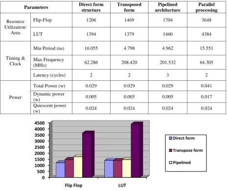
Results obtain for FIR filter (Low Pass Filter tap-20) with different architectures. Table 2 Results
Parameters Direct form structure
Transposed form
Pipelined architecture
Parallel processing
Resource Utilization/
Area
Flip-Flop 1206 1469 1704 3648
LUT 1394 1379 1460 4384
Timing & Clock
Min Period (ns) 16.055 4.798 4.962 15.551
Max Frequency
(MHz) 62.286 208.420 201.532 64.305
Latency (cycles) 2 2 3 2
Power
Total Power (w) 0.029 0.029 0.029 0.041
Dynamic power
(w) 0.005 0.005 0.005 0.017
Quiescent power
(w) 0.024 0.024 0.024 0.024
Figure7 Resource utilization
0 500 1000 1500 2000 2500 3000 3500 4000 4500
Flip Flop LUT
Direct form
Transpose form
Fig 7 shows resources utilization better with pipelined filter in which we introduce delay element between adders, if we see slice/ logic block which consist of LUT & D-f/f introducing delay means enabling flip flop. So, it will not affect area on FPGA.
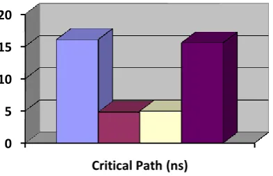
Figure8 Minimum Period(ns)
Minimizing critical path means longest path between input-output without delay element or longest path between input and delay. Referring fig 8 transpose form gives minimum critical path shown in fig 5 longest path is TM+TA (TM : time taken by multiplier & TA : time taken by adder) over direct form i.e. TM+(N-1)TA (N-tap). Again for pipelined & parallel filter there is short computational time.
Figure9 Maximum Frequency (MHz)
Clock frequency bonded by critical path as shown in fig 9 maximum frequency. For transpose form and pipelines filter frequency is maximum but again there must be compromise between other parameters such as resource utilization, etc.
Figure10 Power Consumption
0 5 10 15 20
Critical Path (ns)
Direct form Transpose form Pipelined
Parallel Processing
0 50 100 150 200 250
Maximum Frequency(MHz)
Direct form Transpose form Pipelined
Parallel Processing
0 5 10 15 20 25 30 35 40 45
Power(mW)
Direct form
Transpose form
pipeline
VI.CONCLUSION
Analysing result table 2 we can say that transposed form better which has maximum frequency and short latency but as we discussed limitation, due to capacitive load problem of delay at input and power consumption. Resources utilized by pipelined filter i.e. less number of flip-flops and look up tables (LUTs) with penalty of increased latency. Parallel processing increased throughput result shown for three levels of parallelism means three samples are processed in a single clock cycle i.e. sampling frequency increased. Using combination of pipeline and parallel processing power consumption can further reduced.
REFERENCES
[1] K.K.Parhi. VLSI Digital Signal Processing Systems: Design and Implementation. Wiley, 1999.
[2] R.Tessier ,W.Burleson, “Reconfigurable Computing for Digital Signal Processing : A Survey” , Journal of VLSI Signal Processing 28, 7–27, 2001.
[3] Mahesh Kadam, Kishor Sawarkar, “An Overview of Reconfigurable Hardware for Efficient Implementation of DSP Algorithms”, IOSR Journal of Engineering (IOSRJEN), ISSN (e): 2250-3021, ISSN (p): 2278-8719, Vol. 04, Issue 02, ||V5|| PP 34-43, February 2014.
[4] R. Nanda, C.H. Yang, and D.Markovic. DSP architecture optimization in MATLAB/Simulink environment. To appear at the 2008 VLSI Symposium on Circuits, 2008.
[5] Krishnapriya P.N, ArathyIyer, “Power and Area Efficient Implementation for Parallel FIR Filters Using FFAs and DA”, IJAREEIE, Vol. 2, Special Issue 1, December 2013.
[6] K. Azadet, "Zero-latency pipeline architecture for digital filters." U.S. Patent No. 5,983,254. 9 Nov. 1999.