Design and Implementation of Efficient Carry
Select Adder in QCA
N.Suresh1, Dr B. Prabhakara Rao2
M.Tech Scholar, Dept. of Electronics & Communication, University College of Engineering, Kakinada(Autonomous),
AP, India1
Professor, Dept. of Electronics & Communication, University College of Engineering, Kakinada (Autonomous),
AP, India2
ABSTRACT: In this brief, the logic operations involved in conventional carry select adder (CSLA) and binary to excess-1 converter (BEC)-based CSLA are analyzed to study the data dependence and to identify redundant logic operations. We have eliminated all the redundant logic operations present in the conventional CSLA and proposed a new logic formulation for CSLA. In the proposed scheme, the carry select (CS) operation is scheduled before the calculation of final-sum, which is different from the conventional approach. Bit patterns of two anticipating carry words (corresponding to cin = 0 and 1) and fixed cin bits are used for logic optimization of CS and generation units. An efficient CSLA design is obtained using optimized logic units. The proposed CSLA design involves significantly less area and delay than the recently proposed BEC-based CSLA. Due to the small carry-output delay, the proposed CSLA design is a good candidate for square-root (SQRT) CSLA. Here we are implementing one new carry select adder by using QCA (Quantum-Dot Cellular Automata) in efficient way compared to existing methodologies. As transistors decrease in size more and more of them can be accommodated in a single die, thus increasing chip computational capabilities. However, transistors cannot get much smaller than their current size. The quantum-dot cellular automata (QCA) approach represents one of the possible solutions in overcoming this physical limit, even though the design of logic modules in QCA is not always straightforward. In this brief, we propose a new adder that outperforms all state-of-the art competitors and achieves state-of-the best area-delay tradeoff.
KEYWORDS: Aging effects, Aging indicators, Adaptive hold logic (AHL), Bias Temperature Instability, reliable multiplier, variable latency, fixed latency.
I. INTRODUCTION
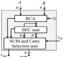
RCA is the slowest in all adders (O (n) time) but it is very compact in size (O (n) area). If the ripple carry adder is implemented by concatenating N full adders, the delay of such an adder is 2N gate delays from Cin to Cout. The delay of adder increases linearly with increase in number of bits. Block diagram of RCA is shown in figure 1. In digital adders, the speed of addition is limited by the time required to propagate a carry through the adder. The sum for each bit position in an elementary adder is generated sequentially only after the previous bit position has been summed and a carry propagated into the next position. The CSLA is used in many computational systems to alleviate the problem of carry propagation delay by independently generating multiple carries and then select a carry to generate the sum [1]. However, the CSLA is not area efficient because it uses multiple pairs of Ripple Carry Adders (RCA) to generate partial sum and carry by considering carry input Cin=0 and Cin=1 then the final sum and carry are selected by the multiplexers (mux). The basic idea of this work is to use Binary to Excess-1 Converter (BEC) instead of RCA with Cin=1 in the regular CSLA to achieve lower area and power consumption [2]–[4]. The main advantage of this BEC logic comes from the lesser number of logic gates than the n-bit Full Adder (FA) structure.
II. LITERATURE SURVEY
III. EXISTING METHODOLOGIES
The CSLA has two units: 1) the sum and carry generator unit (SCG) and 2) the sum and carry selection unit [9]. The SCG unit consumes most of the logic resources of CSLA and significantly contributes to the critical path. Different logic designs have been suggested for efficient implementation of the SCG unit. We made a study of the logic designs suggested for the SCG unit of conventional and BEC-based CSLAs of [6] by suitable logic expressions. The main objective of this study is to identify redundant logic operations and data dependence. Accordingly, we remove all redundant logic operations and sequence logic operations based on their data dependence.
Fig. 3. (a) Conventional CSLA; n is the input operand bit-width. (b) The logic operations of the RCA is shown in split form, where HSG, HCG, FSG, and FCG represent half-sum generation, half-carry generation, full-sum generation, and full-carry generation,
respectively.
Fig. 4. Structure of the BEC-based CSLA; n is the input operand bit-width.
Fig. 5. (a) Proposed CS adder design, where n is the input operand bit-width, and [∗] represents delay (in the unit of inverter delay), n = max(t, 3.5n + 2.7). (b) Gate-level design of the HSG. (c) Gate-level optimized design of (CG0) for input-carry = 0. (d) Gate-level
optimized design of (CG1) for input-carry = 1. (e) Gate-level design of the CS unit. (f) Gate-level design of the final-sum generation (FSG) unit.
word s0 and half-carry word c0 of width n bits each. Both CG0 and CG1 receive s0 and c0 from the HSG unit and generate two n-bit full-carry words c01 and c11 corresponding to input-carry ‘0’ and ‘1’, respectively. The logic diagram of the HSG unit is shown in Fig. 5(b). The logic circuits of CG0 and CG1 are optimized to take advantage of the fixed input-carry bits. The optimized designs of CG0 and CG1 are shown in Fig. 5(c) and (d), respectively. The CS unit selects one final carry word from the two carry words available at its input line using the control signal cin. It selects c01 when cin = 0; otherwise, it selects c11. The CS unit can be implemented using an n-bit 2-to-l MUX. However, we find from the truth table of the CS unit that carry words c01 and c11 follow a specific bit pattern. If c01 (i) = ‘1’, then c11 (i) = 1, irrespective of s0(i) and c0(i), for 0 ≤ i ≤ n − 1. This feature is used for logic optimization of the CS unit. The optimized design of the CS unit is shown in Fig. 5(e), which is composed of n AND–OR gates. The final carry word c is obtained from the CS unit. The MSB of c is sent to output as cout, and (n − 1) LSBs are XORed with (n − 1) MSBs of half-sum (s0) in the FSG [shown in Fig. 3(f)] to obtain (n − 1) MSBs of final-sum (s). The LSB of s0 is XORed with cin to obtain the LSB of s.
Fig. 6. Proposed SQRT-CSLA for n = 16. All intermediate and output signals are labeled with delay
IV. PROPOSED METHOD
Quantum Dot Cellular Automata (sometimes referred to simply as quantum cellular automata, or QCA) are proposed models of quantum computation, which have been devised in analogy to conventional models of cellular automata introduced by von Neumann. Standard solid state QCA cell design considers the distance between quantum dots to be about 20 nm, and a distance between cells of about 60 nm. Just like any CA, Quantum (-dot) Cellular Automata are based on the simple interaction rules between cells placed on a grid. A QCA cell is constructed from four quantum dots arranged in a square pattern. These quantum dots are sites electrons can occupy by tunneling to them.
Fig 7: Simplified Diagram of QCA Cell
Fig 8: Four Dot Quantum Cell
Fig 9: Structure of Majority gate
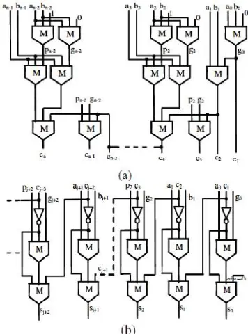
Fig 10: ARCHITECTURE OF BASIC NOVEL 2-BIT ADDER
To introduce the novel architecture proposed for implementing ripple adders in QCA, let consider two n-bit addends A
= an−1, . . . , a0 and B = bn−1, . . . , b0 and suppose that for the i th bit position (with i = n − 1, . . . , 0) the auxiliary propagate and generate signals, namely pi = ai + bi and This article has been accepted for inclusion in a future issue of this journal. Content is final as presented, with the exception of pagination.gi = ai · bi , are computed. ci being the carry produced at the generic (i−1)th bit position, the carry signal ci+2,furnished at the (i+1)the bit position.
Fig 11: Novel n-bit adder (a) carry chain and (b) sum block.
And also here we are designed multiplier and accumulator unit by using the existing and proposed CSLA.
V. SIMULATION RESULTS
Fig 12: Output waveform for SQRT CSLA
Fig 13: Output waveform for Proposed QCA Adder
Fig 14: Output waveform for Multiplier and Accumulator
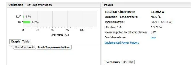
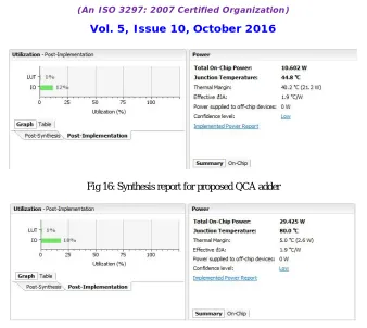
Fig 16: Synthesis report for proposed QCA adder
Fig 17: synthesis report for proposed multiplier and accumulator
VI. CONCLUSION
The reduced number of gates of this work offers the great advantage in the reduction of area and also the total delay. The QCA architecture is therefore, low area, low delay, simple and efficient for VLSI hardware implementation. And we have also analyzed the logic operations involved in the conventional and BEC-based CSLAs to study the data dependence and to identify redundant logic operations. We have eliminated all the redundant logic operations of the conventional CSLA and proposed a new logic formulation for the CSLA. In the proposed scheme, the CS operation is scheduled before the calculation of final-sum, which is different from the conventional approach. Carry words corresponding to input-carry ‘0’ and ‘1’ generated by the CSLA based on the proposed scheme follow a specific bit pattern, which is used for logic optimization of the CS unit. Fixed input bits of the CG unit are also used for logic optimization. Based on this, an optimized design for CS and CG units are obtained. Using these optimized logic units, an efficient design is obtained for the existed CSLA. The CSLA design involves significantly less area and delay than the recently proposed BEC-based CSLA. Due to the small carry output delay, the proposed CSLA design is a good candidate for the SQRT adder.
REFERENCES
[1] C. S. Lent, P. D. Tougaw, W. Porod, and G. H. Bernestein, “Quantum cellular automata,” Nanotechnology, vol. 4, no. 1, pp. 49– 57, 1993.
[2] M. T. Niemer and P. M. Kogge, “Problems in designing with QCAs Layout = Timing,” Int. J. Circuit Theory Appl., vol. 29, no. 1,pp. 49–62, 2001.
[3] J. Huang and F. Lombardi, Design and Test of Digital Circuits by Quantum-Dot Cellular Automata. Norwood, MA, USA: Artech House,2007.
[4] W. Liu, L. Lu, M. O’Neill, and E. E. Swartzlander, Jr., “Design rules for quantum-dot cellular automata,” in Proc. IEEE Int. Symp. Circuits Syst., May 2011, pp. 2361–2364.
[5] K. Kim, K. Wu, and R. Karri, “Toward designing robust QCA architectures in the presence of sneak noise paths,” in Proc. IEEE Design, Autom. Test Eur. Conf. Exhibit., Mar. 2005, pp. 1214–1219.
[7] K. Walus, G. A. Jullien, and V. S. Dimitrov, “Computer arithmetic structures for quantum cellular automata,” in Proc. Asilomar Conf.Sygnals, Syst. Comput., Nov. 2003, pp. 1435–1439.
[8] K. K. Parhi, VLSI Digital Signal Processing. New York, NY, USA:Wiley, 1998.
[9] A. P. Chandrakasan, N. Verma, and D. C. Daly, “Ultralow-power electronics for biomedical applications,” Annu. Rev. Biomed. Eng., vol. 10, pp. 247–274, Aug. 2008.
[10] O. J. Bedrij, “Carry-select adder,” IRE Trans. Electron. Comput., vol. EC-11, no. 3, pp. 340–344, Jun. 1962.
[11] Y. Kim and L.-S. Kim, “64-bit carry-select adder with reduced area,” Electron. Lett., vol. 37, no. 10, pp. 614–615, May 2001. [12] Y. He, C. H. Chang, and J. Gu, “An area-efficient 64-bit square root carry select adder for low power application,” in Proc. IEEE Int. Symp. Circuits Syst., 2005, vol. 4, pp. 4082–4085.
[13] B. Ramkumar and H.M. Kittur, “Low-power and area-efficient carry-select adder,” IEEE Trans. Very Large Scale Integr. (VLSI) Syst., vol. 20, no. 2, pp. 371–375, Feb. 2012.
[14] I.-C. Wey, C.-C. Ho, Y.-S. Lin, and C. C. Peng, “An area-efficient carry select adder design by sharing the common Boolean logic term,” in Proc. IMECS, 2012, pp. 1–4.
[15] S.Manju and V. Sornagopal, “An efficient SQRT architecture of carry select adder design by common Boolean logic,” in Proc. VLSI ICEVENT, 2013, pp. 1–5.