ABSTRACT
CHAUHAN, VIKAS. Code Modulated Interferometric Imaging System using Phased Arrays. (Under the direction of Brian A. Floyd.)
Millimeter-wave (mm-wave) imaging provides compelling capabilities for security
screening, navigation, and bio-medical applications. Traditional scanned or focal-plane
mm-wave imagers are bulky and costly. In contrast, phased-array hardware developed for
mass-market wireless communications and automotive radar promise to be extremely low
cost. This work presents techniques which can allow low-cost phased-array receivers to
be reconfigured or re-purposed as interferometric imagers, removing the need for
cus-tom hardware and thereby reducing cost. Since traditional phased arrays power combine
incoming signals prior to digitization, orthogonal code-modulation is applied to each
incoming signal using phase shifters within each front-end and two-bit codes. These
code-modulated signals can then be combined and processed coherently through a shared
hardware path. Once digitized, visibility functions can be recovered through squaring and
code-demultiplexing operations. Provided that codes are selected such that the product of
two orthogonal codes is a third unique and orthogonal code, it is possible to demultiplex
complex visibility functions directly. As such, the proposed system modulates incoming
signals but demodulates desired correlations.
Firstly, we present the operation of the system, a validation of its operation using
be-havioral models of a traditional phased array and a benchmarking of the code-modulated
interferometer against traditional interferometer using simulation results and sensitivity
analysis. Secondly, for the proof of concept with a prototype, we present a simple CMI
sys-tem operating in the license-free 60-GHz band using a four-element phased-array receiver
four-element 60-GHz phased array chip is wire-bonded onto a Rogers-5880 substrate board
with on-board slot antennas, and a single 60-GHz output is measured using a power
detec-tor. This scalar measurement is then demodulated to obtain the interferometric visibilities.
The four-element phased array is thinned to obtain a 13-pixel image and the system is
demonstrated through a point-source detected at different locations.
Finally, the operation and capabilities of code-modulated interferometry (CMI) are
demonstrated at 10-GHz using commercially-available phased arrays. A 33-pixel,
eight-element prototype is created using two commercially-available ADAR1000 phased-array
receivers from Analog Devices Inc. The chips are connected at board level to a patch antenna
array. The serial interface is used to apply codes whereas the on-chip power detector and
data converter are used for direct read out of the composite code-multiplexed imaging
data. These are then processed off-line in MATLAB to reconstruct the image. The 33-pixel
camera is demonstrated in hardware for point-source detection. Further to demonstrate
the scalability of the concept, a 16-element, 169-pixels CMI imaging system is presented at
10-GHz using the four of the same commercially-available phased arrays from ADI. Two
© Copyright 2019 by Vikas Chauhan
Code Modulated Interferometric Imaging System using Phased Arrays
by Vikas Chauhan
A dissertation submitted to the Graduate Faculty of North Carolina State University
in partial fulfillment of the requirements for the Degree of
Doctor of Philosophy
Electrical Engineering
Raleigh, North Carolina
2019
APPROVED BY:
Paul Franzon John Muth
Chih-Hao Chang Brian A. Floyd
DEDICATION
To the Queen of Vrndavana:
tapta-kancana-gaurangi radhe vrndavanesvari
vrsabhanu-sute devi pranamami hari-priye
"I offer my respects to Radharani whose bodily complexion is like molten gold and who is
the Queen of Vrndavana. You are the daughter of King Vrsabhanu, and You are very dear to
BIOGRAPHY
Vikas Chauhan was born in Sisana (District Baghpat), U.P., India. He grew up in Gurgaon
(now Gurugram), Haryana, India.
Vikas received the B.E.(Hons.) degree in electrical and electronics engineering from Birla
Institute of Technology and Science (BITS - Pilani), India, in Spring 2012. In Fall 2012, he
enrolled in the Master of Science (M.S.) program in electrical engineering at North Carolina
State University, Raleigh, NC, USA. In 2013, he joined Professor Brian Floyd’s iNtegrated
Circuits and Systems lab at NC State (iNCS2) and transferred into the Ph.D. program in 2014. He received his en-route M.S. degree in 2014.
Vikas completed two internships during his time at NC State University. He was an intern
at Qualcomm Corp. R&D, Qualcomm Technologies, Inc., San Diego, CA, USA in summer
2017 where he worked on milli-meter wave integrated circuit (mm-wave IC) design for
5G-communication. In spring 2019, he interned at imec USA Nanoelectronics Design Center
Inc., FL, USA where he worked on mm-wave IC design for imaging applications. He will
be joining full-time as a researcher at imec USA in fall 2019. His research interests include
ACKNOWLEDGEMENTS
First, I would like to thank my advisor Dr. Brian Floyd for this untiring help, mentorship and
support during my time at NC State University. I would also like to thank Dr. Paul Franzon,
Dr. John Muth and Dr. Chih-Hao Chang for serving on my committee, and their valuable
time and comments.
I would like to thank everyone involved in the CoMET and IRIS projects: Zhangjie Hong,
Simon Schönherr, Dr. Kevin Greene, Dr. Dong Gun Kam, Haekyo Seo and Dr. Zhengxin
Tong who contributed in this research and working with whom has been a pleasure. I
am grateful to Dr. Yi-Shin Yeh, Dr. Charley Wilson, Dr. Weihu Wang, Dr. Anirban Sarkar,
Jeff Bonner-Stewart, Tiantong Ren, Yuan Chang, and all my other colleagues at iNCS2for technical discussions and their readiness to always help and support me.
My friends and fellow Ph.D. students, Sandeep Hari, Dr. Deeksha Lal, Kirti Bhanushali,
Munirah Boufarsan and Dr. Viswanath Ramesh for making my time inside and outside MRC
enjoyable. My dearest friends Shalki Shrivastava, Nirmaan Aggarwal, Varun Joshi, Marian
Mersmann, Crystal Hilton, and my other friends who made my life in NC memorable.
I would like to thank my family for their love, support and patience.
Lastly, I would like to thank everyone who has helped in one way or other in this research
and my journey as a graduate student.
The material in this thesis is based upon work partially supported by the DARPA Young
Faculty Award (N66001-11-1-4144), the 2015 Chancellor’s Innovation Fund at NCSU, the
Army Small Business Innovation Research (SBIR) Program Office under contract no.
W31P4Q-17-C-0020, the AFRL and DARPA under agreement FA8650-16-1-7629, GlobalFoundries
TABLE OF CONTENTS
LIST OF TABLES . . . vii
LIST OF FIGURES. . . viii
Chapter 1 Introduction. . . 1
1.1 Research Objectives . . . 5
Chapter 2 Code-modulated Interferometry. . . 7
2.1 Interferometry Fundamentals . . . 7
2.2 Code-Modulated Interferometry with Phased Arrays . . . 10
2.2.1 Modulation of Antenna Responses . . . 10
2.2.2 Demodulation of Complex Visibility Functions . . . 12
2.3 Balanced-Orthogonal-Code-Products (BOCP) . . . 16
2.3.1 Rademacher Codes . . . 16
2.3.2 Hadamard-Walsh Codes . . . 17
2.3.3 Gold Codes . . . 18
2.4 Behavioral Models . . . 21
2.4.1 One-dimensional CMI . . . 21
2.4.2 Two-dimensional CMI . . . 30
2.5 Sensitivity Analysis . . . 33
2.6 Conclusion . . . 38
Chapter 3 Demonstration using In-house 60-GHz Phased Array . . . 39
3.1 Overview . . . 39
3.2 Four-element Code-modulated Interferometry . . . 40
3.3 60-GHz Hardware Prototype . . . 44
3.3.1 Circuit Architecture . . . 44
3.3.2 Packaging . . . 50
3.3.3 Thinned Antenna-Array Design . . . 56
3.4 Imaging Experiment and Results . . . 59
3.4.1 Demonstration Setup . . . 59
3.4.2 Code-Modulation, Data Acquisition, and Processing . . . 61
3.4.3 Results . . . 63
3.5 Conclusion . . . 68
Chapter 4 Imaging System Prototypes using COTS Phased Arrays . . . 69
4.1 Overview . . . 69
4.2 Code-Modulated Interferometry in COTS Phased Arrays . . . 72
4.3.1 Eight-Channel Phased Array . . . 74
4.3.2 Sparse Antenna Array . . . 76
4.3.3 Calibration of Array . . . 80
4.3.4 Code-Modulation, Data Acquisition, and Processing . . . 83
4.3.5 Imaging Experiment and Results . . . 86
4.4 169-Pixel COTS CMI Imaging Prototype . . . 93
4.4.1 Sparse Antenna Array . . . 93
4.4.2 Imaging Experiment and Results . . . 95
4.5 Conclusion . . . 99
Chapter 5 Conclusion and Future work . . . 103
5.1 Summary and Conclusions . . . 103
5.2 Comparison with Existing Solutions . . . 105
5.3 Key Research Contributions . . . 107
5.4 Future Work . . . 108
BIBLIOGRAPHY . . . 110
APPENDICES . . . 117
Appendix A MATLAB Codes and Design Files . . . 118
A.1 MATLAB Codes . . . 118
A.1.1 Code for 3-D Path Length . . . 118
A.1.2 Code for Image Data Processing . . . 121
A.1.3 Code to Generate BOCP Walsh-Hadamard Codes . . . 129
A.2 Gold Code Circuit Design . . . 132
A.3 High Frequency Board Design Files . . . 136
Appendix B A 24-44 GHz UWB 5G LNA . . . 138
B.1 Motivation . . . 138
B.2 Design . . . 140
B.3 Measurement Results . . . 143
B.4 Comparison and Discussion . . . 146
LIST OF TABLES
Table 2.1 Feedback connections for m-sequences[Gar10]. . . 19 Table 2.2 Gold codes using different sifts[DJ96]. . . 21
Table 3.1 Matrix showing the combinations of in-phase and quadrature-phase signals needed to be multiplied to obtain real and imaginary compo-nents of visibility samples. . . 43 Table 3.2 Measured performance summary for a single channel of the 60GHz
phased array . . . 53
Table 5.1 Comparison metrics for code-modulated interferometric imaging system with conventional imaging systems. . . 106 Table 5.2 Comparison of CMI imaging systems with published conventional
imaging systems. . . 106
LIST OF FIGURES
Figure 2.1 Schematic of the measurement of a visibility sample[Sim18]. . . 9 Figure 2.2 (a) Block diagram of a conventional interferometric array and (b)
Block diagram of a conventional phased array employing RF phase shifting and combining. . . 10 Figure 2.3 Block diagram of a code-modulated interferometric imaging system
employing code-modulation within each phase shifter of a phased array and baseband visibility demodulation using a bank of correlators. 13 Figure 2.4 Block diagram of a code-modulated interferometric imaging system
employing code-modulation within each phase shifter of a phased array and baseband visibility demodulation using code products. . . 13 Figure 2.5 A four stage shift register with one tap generating an m-sequence
[Gar10]. . . 19 Figure 2.6 Two LFSR producing m-sequences Seq 1 and Seq 2 used to generate
a Gold code[DJ96]. . . 20 Figure 2.7 Behavioral model for one-dimensional code-modulated
Interferom-etry. . . 22 Figure 2.8 SIMULINK behavioral model for fifteen elements one-dimensional
code-modulated interferometry. . . 23 Figure 2.9 SIMULINK behavioral model for fifteen elements 1D CMI showing
noise point source, front end model and code-modulation. . . 24 Figure 2.10 SIMULINK behavioral model for fifteen elements 1D CMI showing
power combining and squaring operations. . . 25 Figure 2.11 SIMULINK behavioral model for fifteen elements 1D CMI showing
demodulation using matched filters (code-products) and integration. 26 Figure 2.12 SIMULINK behavioral model for fifteen elements 1D basic
interfer-ometry showing a bank of complex correlators to obtain complex visibility samples. . . 27 Figure 2.13 Behavioral modeling results comparing traditional to code-modulated
interferometry: (a)-(d) shows the results of a point source at 20◦, 30◦,
40◦, and 50◦elevation angles; (e) and (f ) show code-modulated
inter-ferometry resolving two point sources at elevation angles 20◦and 30◦ in (e), and 30◦and 40◦in (f ). . . . 29
Figure 2.14 Behavioral model for two-dimensional code-modulated interferom-etry. . . 31 Figure 2.15 Simulation results for imaging 2-D sources with code modulated
Figure 3.1 Zero redundancy interferometric array using four antennas. The an-tennas are spaced atλ, 3λand 2λ, producing baselines of length of 0−6λ. . . 41 Figure 3.2 Schematic of the 5-stage LNA using stagger-tuned current-sharing
common-source amplifiers[Gre18]. . . 46 Figure 3.3 MeasuredS-parameters for the LNA break-out circuit used in the
phased array as compared to simulated results.[Gre18]. . . 46 Figure 3.4 Block diagram of the active vector interpolator topology implemented
as each elements’ phase shifter[Gre18]. . . 47 Figure 3.5 Schematic of the vector interpolator using cross-coupled Gilbert cells
to form the variable-gain amplifiers[Gre18]. . . 48 Figure 3.6 Power detector schematic used to square the combined code-modulated
signals and generate a low-frequency signal to be captured by an ex-ternal data converter[Gre18]. . . 49 Figure 3.7 Block diagram of the four-element phased array receiver[Gre18; Gre17]. 51 Figure 3.8 Die photo. The total area is 3 mm x 1.3 mm[Gre18; Gre17]. . . 52 Figure 3.9 MeasuredS-parameters compared to simulated results for element
one of phased array for the 0-degree phase setting[Gre18; Gre17]. . . 52 Figure 3.10 Stack-up of printed-circuit board. . . 53 Figure 3.11 HFSS simulation of G-S-G wirebonds. . . 54 Figure 3.12 EM structures for (a) antennas with feedlines; and (b) wire-bonds,
compensation, and CPW-to-microstrip transition. . . 55 Figure 3.13 Simulated (a) input return loss and (b) gain radiation pattern (in dB,
vstheta at phi=0 deg., 60 GHz) for antennas. . . 58 Figure 3.14 Block diagram of imaging setup. . . 60 Figure 3.15 Photographs of board, 60-GHz phased array, and overall experimental
setup. The board size is 60 x 36 mm2. . . . 60 Figure 3.16 Simulated (a) feedline loss in dB and (b) phase.S51for E1,S62for E2,
S73for E3, andS84for element E4. . . 62 Figure 3.17 Normalized brightness plots for point source at azimuthal angle of
approximately 0◦. . . 64 Figure 3.18 Measured and simulated normalized brightness plots for point source
at azimuthal angle of approximately (a) 0◦(b) 5◦(c) 10◦(d) 20◦(e) 25◦
(f ) -10◦(g) -20◦(h) -30◦[Cha p]. . . 65 Figure 3.19 Gain radiation pattern of elements (a) E1, (b) E2, (c) E3 and (d) E4. . 66 Figure 3.20 Gain radiation pattern of the four element array. . . 67 Figure 3.21 Brightness simulation with (a) two point sources at 0◦and 10◦; and
(b) 22 dB receiver NF before and after noise calibration. . . 68
Figure 4.2 Block diagram of ADAR1000 chip showing four TX (TX1 - TX4) and four RX (RX1-RX4)[Adaa]. . . 75 Figure 4.3 Photo of ADAR1000 EVAL board showing four TX (TX1 - TX4) and
four RX (RX1-RX4)[Adab]. . . 76 Figure 4.4 Photo of the available patch antenna board with 16 linearly λ/2
spaced antenna elements. . . 76 Figure 4.5 Gain, directivity, and efficiency of a single patch antenna, provided
by ADI[Ana]. . . 77 Figure 4.6 (a) Beam-width and (b) input match of a single patch antenna,
pro-vided by ADI[Ana]. . . 77 Figure 4.7 Sparsely sampled antenna configuration for one-dimensional
imag-ing illustratimag-ing all available baselines[Sim18]. . . 79 Figure 4.8 Sampled (u,v)-space for the used antenna configuration in one
di-mension[Sim18]. . . 80 Figure 4.9 (a) Photograph of prototype front view showing antennas. (b) Plot
indicating the sampledu-vspace. . . 81 Figure 4.10 Example plot for post-calibration gain of eight RX channels. . . 83 Figure 4.11 Representative ADC output for four-element linear array with code
length of 256. . . 85 Figure 4.12 Photographs of experimental setup of 10 GHz imager. . . 87 Figure 4.13 Normalized brightness plots for different point source positions: (a)
0◦(b) -15◦(c) 30◦(d) -40◦(e) 60◦(f ) 70◦. . . 89 Figure 4.14 Point spread function: Normalized brightness plots for (elevation,
azimuthal) angle 0◦, 0◦.N =11 andM =3. . . . 90
Figure 4.15 Normalized brightness plots for (elevation, azimuthal) angle (a) 0◦, 10◦ (b) 0◦, 20◦ (c) 0◦, -10◦(d) 0◦, -30◦(e) 10◦, 0◦(f ) -10◦, -30◦ (g) -10◦,
40◦(h) 10◦, -50◦.N =11 andM =3. . . . 92
Figure 4.16 (a) Antenna array layout and (b) the corresponding UV spacing[Ton15]. 94 Figure 4.17 (a) Photograph of four ADAR1000 EVAL boards connected together
(b) Sparsely sampled 16-antenna array. . . 95 Figure 4.18 Setup for 16-elements imaging experiment. . . 97 Figure 4.19 Photographs of two horn antennas as point sources to demonstrate
resolution. . . 98 Figure 4.20 Images taken for two point sources separately at different locations
and together. . . 100 Figure 4.21 Images of two point sources moving closer to demonstrate resolution.101
condi-Figure A.4 Layout of code generator. . . 134
Figure A.5 Simulation result showing the Seq1, Seq2 and 0-Shift, 1-Shift, 2-Shift and 3-Shift combinations. . . 135
Figure A.6 High frequency board design metal layers. . . 136
Figure A.7 High frequency board design metal layers. . . 137
Figure B.1 Schematic of the NB LNA (biasing details not shown). . . 141
Figure B.2 Schematic of the UWB LNA (biasing details not shown). . . 141
Figure B.4 Noise figure simulation and measurement for UWB LNA. . . 144
CHAPTER
1
INTRODUCTION
Millimeter-wave (mm-wave) energy can penetrate clothing, bandages, packages, fog, and
dust/snow storms due to their small wavelength. As such, mm-wave cameras operating in
the range of 30-300 GHz can be used for numerous applications, including the following:
• Concealed Object Detection:Millimeter-waves go through clothing and are used in
security portals at airports,courthouses, etc., to detect objects hidden on the body
(weapons, drugs, smuggled goods)[Hug97]. The key need today is a lower cost solution
which still provides necessary performance (i.e., resolution, sensitivity). Lower-cost
stations, prisons, etc.
• Aircraft Navigation:Millimeter-waves penetrate clouds and dust storms and can be
used to improve visibility in poor conditions (e.g., helicopter detecting power lines
through a dust storm). Key requirements for a camera mounted on an aircraft are to
reduce size and weight (no lens). Interferometers are ideal for this application[Per07].
• Imaging from UAVs:UAVs or drones represents an emerging market, where mm-wave
imaging could provide unique sensing capabilities, particularly if the imager can
double as a radar or radio system.
• Biomedical:Millimeter-waves may also be used for biomedical imaging. For
exam-ple, it may be possible to image through bandages to monitor the healing of dry
wounds such as burns without removing the bandage. Millimeter-wave cameras
could also measure skin temperature through clothing and allow for diagnosis of
conditions related to poor circulation such as compartment syndrome or over- or
under-resuscitation. High sensitivity and small cameras are required. These could be
deployed to hospitals and doctors’ offices.
• Quality-Control:Millimeter-waves can penetrate certain types of packaging material
and a camera could be used to provide quality control within a manufacturing line to
assess the condition or presence of a product.
• Wireless Clothes Fitting:Millimeter-wave cameras provide an ability to see through
clothes and remotely measure a person’s size for use in clothing stores. Key needs
would include privacy and low system cost.
The imaging systems that work with ambient mm-wave energy are called passive
imagers[Tho06]. Every object above the absolute zero temperature emits radiation, called
as black body radiation or thermal radiation that carry intrinsic information about the body
and can be used for imaging. Since the passive imaging is non-intrusive and non-invasive, it
is considered a safe way of inspection. Such an inspection is preferred at mm-wave
frequen-cies (94 GHz[Ton15]or higher) for high resolution. Millimeter-wave imagers are widely
used at airports for security screening[TSAb; TSAa]. Due to all the above listed applications
and advantages, there is an increasing interest in mm-wave imaging systems.
A variety of mm-wave imaging systems have been developed to date[Yuj06; Yeo11;
Let03; Dow96; She01; Lyo; Ahm; Kol05; Mil; Sin01; Sat09; Int]. Existing passive mm-wave
imagers are able to achieve a sensitivity as low as 0.28 K[Sin01], as well as a frame rate
as high as 10-17 frames per second[Yuj06; VD06; Miz05]. Many of these use mechanical
scanning[Kol05; Mil; Sin01; Sat09], mirrors for scanning[VD06; Yuj06], electronic beam
forming and scanning or focal-plane arrays (FPA). These cameras can be bulky due to
the use of an external lens[Miz05; Sat09]and expensive due to the reliance on custom
compound-semiconductor hardware for scanned solutions[Uzu13; MR10a]or the need
for a large number of detecting elements in FPA solutions. Also, any kind of mechanical or
electronic scanning may slow down the system making it unsuitable for video frame rates.
An alternative approach which has the potential to reduce both camera volume and
camera cost is to shift to interferometry. Interferometry or synthetic aperture radiometer
(SAR)[Tho08; HA00; Nar96]eliminates the need for a lens since angle-of-arrival
informa-tion is obtained through complex correlainforma-tions or visibilities. Furthermore, the number of
required elements is reduced, since N elements can be used to obtainNC2correlations. A drawback of interferometry is the more complicated image processing arising from the
both high-performance mm-wave transistors and dense low-power digital computation
[Per07]. These requirements can now be met in today’s advanced silicon technologies,e.g.,
130-nm SiGe BiCMOS, 65-nm CMOS and beyond, which feature transistors havingfT and
fM AX in excess of 200 GHz.
While it is possible to develop a highly-integrated mm-wave interferometer in silicon,
such a customized circuit would require non-negligible development costs. Also, if the total
mm-wave camera market volume remains low, the unit cost would remain high. The low
cost of imaging system is crucial for mass deployment in certain applications. In contrast to
this, high-volume mm-wave applications are emerging[Kla14; Wan14; Sha19], including
60-GHz phased arrays for short-range multi-Gb/s wireless links[60s; Nat11; Kri10; Wu14]and
77-GHz phased arrays for automotive radar systems[Ku13; Lee10; Mit10; Has12]. Moreover,
due to the increasing interest in 5G applications, more of such hardware will be available
commercially for a fraction of cost today. These commercial-of-the-shelf (COTS) phased
arrays have the potential to be used in other multi-antenna applications, allowing for
substantial cost reduction. In this work, we explore the possibility of turning a COTS phased
array receiver into an interferometric imaging receiver using code-modulation.
Code-modulated interferometry (CMI)[Cha16]is an alternative that employs thinned
apertures to reduce the hardware requirement and repurposes communication phased
arrays to reduce development costs. In CMI, the complex visibility samples are obtained
by orthogonal code-modulation of individual signals using phase shifters, processing of
combined signals using the shared receiver path, creation and detection of complex
code-multiplexed visibilities using a scalar power detector, and demodulating all individual
visibilities using appropriate code products.
The use of code-modulation within receivers has been studied in prior work in the
been used within correlating interferometers to eliminate unwanted performance artifacts
such as LO feedthrough or spurious signals[Tho08]. Second, for communications, code
modulations have been applied within a receiver to allow multiple receiver element to share
a common hardware path[Tze09]; however, the concepts in[Tze09]were not implemented
within an N-element phased array. Our demodulation approach which recovers correlations
rather than signals further distinguishes our work over this prior art.
Note that a similar coded imaging approach, referred to as compressive synthetic
aper-ture interferometric radiometer, is presented in[Kpr18].M antenna channels are coded
intoN measured signals (N <<M receivers) using a passive microwave device such as a
resonant cavity. In contrast to[Kpr18], the CMI approach does not require bulky microwave
cavities and enables application of software-programmable codes. Also, CMI enables the
codes to be modified in software, providing flexibility to change the codes based on the
application. Finally, CMI can employ a simple scalar (power) detector as a direct
mea-surement, eliminating the need for complex correlators and hence compact, has a single
receiver channel (N =1), requires only one scalar measurement from power detector, and
has active coding with ability to upgrade codes as they evolve. The possible disadvantage
in CMI compared to[Kpr18]is its lower sensitivity since all signals are combined into one
shared signal for processing.
1.1
Research Objectives
The objectives of this work are to investigate code-modulated interferometry as a method
to re-purpose phased arrays into imaging system and build the hardware to demonstrate
the theoretical and behavioral model results, formulate sensitivity and evaluate image
This document is organized into five chapters. Chapter 1 presents the introduction to
the topic and motivation behind this work. Chapter 2 presents the theoretical investigation
and modeling of code-modulated interferometry. Chapter 3 presents a millimeter-wave
implementation using in-house 60 GHz phased array. The millimeter-wave imaging
proto-type demonstrates the code-modulated interferometry for a simple four-element system.
Chapter 4 presents an eight-element 10 GHz prototype of code-modulated
interferomet-ric imaging using commercially available phased arrays. Further, Chapter 4 discusses the
scalability and expands the 10 GHz eight-element imager in to a true two-dimensional
16-elements imager and demonstrates the resolution of two point sources. Finally, Chapter
5 presents the conclusions and summary of the completed work, and the scope for future
CHAPTER
2
CODE-MODULATED INTERFEROMETRY
2.1
Interferometry Fundamentals
As is well known, interferometry is a technique used by radio astronomers to realize higher
resolution telescopes using a sparse array of coherent detectors to sample an aperture
[Tho08]. Measurements are made by cross correlating the signals from spatially separated
pairs of antennas (a baseline) with overlapping field-of-view (FOV) known as visibility
samples. Measurements for different baselines, collectively known as the visibility function,
V(u,v) = Z 2π
0 Z π
0
TΩ(θ,φ)ej2π(u·l+v·m) s i nθ dθ dφ, (2.1) wherel =s i nθc o sφandm=s i nθs i nφ, anduandvbaselines relate to two-dimensional
antenna spacings per unit wavelength.TΩ is obtained using a discrete inverse Fourier
transform of the measured visibility samples. The unit samples in the brightness domain
are inversely related to the unit visibility samples, as shown below, whereN andM are total
number of complex visibility samples inu andv domains respectively[Tho08],
N∆l = (∆u)−1 and M∆m= (∆v)−1. (2.2)
These determine the field-of-view (FOV) and resolution. For a linear array, resolution
is∆s i n(θr e s) = (N∆u)−1 ≈λ/2Dm a x and FOV isN∆s i n(θ) = (∆u)−1 ≈λ/Dm i n , where
Dm a x andDm i n are maximum and minimum antenna spacing respectively[Lim09]. The
maximum antenna spacing (and hence minimum angular resolution) is limited by the
coherence requirement[Let03; Sko06]as follows
Dm a xs i n θm a x <
c
B , (2.3)
wherec is the velocity of light andBis the bandwidth. More details about interferometry,
Nyquist criterion foru-vsampling, correlators and other requirements can be found in
[Tho08; Lim09; Ruf88].
Interferometers must therefore evaluate (complex) correlations for each baseline and
then compute the inverse Fourier transform to obtain the image. Interferometry does not
require a focusing lens, allowing for flat or conformal imagers. Note that image resolution
Figure 2.1Schematic of the measurement of a visibility sample[Sim18].
baselines can be averaged to reduce noise.
Since an interferometer must measure each antenna signal and since the correlations
are typically evaluated in the digital domain, an ideal interferometer array would include
N receive chains in parallel, as shown in Fig. B.3(a). Each chain would generally include a
front-end amplifier, a quadrature downconversion mixer, and baseband analog-to-digital
converters (ADCs). A bank of digital complex correlators would then be used to evaluate all
possible pairwise correlations.
In contrast to this digital-combined array, Fig. B.3(b) shows a simplified block diagram
of a conventional phased array. Each front-end element contains an RF amplifier and
phase-shifter. Individual signals are then added together, downconverted, and processed through
to the digital domain. In comparing the phased array to the ideal interferometer array, we
observe that the interferometer has individual hardware paths per element whereas the
phased array has a shared hardware path beginning at the signal combiner. As a result, any
ADC ADC ADC ADC Complex Correlator I Q I Q LNAs Antenna 1 Antenna N θ θ θ θ C O M B I N E R IF and Baseband Circuitry Mixer Frontends Antenna 1 Antenna N (a) (b)
Figure 2.2(a) Block diagram of a conventional interferometric array and (b) Block diagram of a conventional phased array employing RF phase shifting and combining.
path, while retaining necessary individual signal information and/or signal correlations.
The proposed solution to overcome this limitation is by using code-modulation technique.
2.2
Code-Modulated Interferometry with Phased Arrays
2.2.1
Modulation of Antenna Responses
A phased array can be reconfigured into an interferometer array by applying orthogonal
coding functions to each incoming signal using the phase shifters present within each
front end. Code modulation allows multiple, individual radiometer data streams to be
multiplexed onto a single hardware path. As will be shown, we can then recover
correla-tions between signals downstream through correlating the aggregate response with code
products.
code-modulated communications (e.g., CDMA), the data signals are modulated with a
code running at a significantly higher frequency than the modulation or symbol rate. For
imaging applications, the signals are being modulated proportional to the scene change;
hence, the code rate can be kept low.
Mathematically, the phase modulation within each front-end can be represented as
sn(t) =Anc o s(ωot +θn−φn), (2.4)
wheresn(t)represents the signal at the output of thent h phase shifter,An andθnrepresent
the amplitude and phase of the signal, andφn represents the phase modulation imparted.
We can subdivide this expression into in-phase (si,n) and quadrature-phase (sq,n) signal
components which are then multiplied by in-phase (in) and quadrature-phase (qn) codes,
as follows:
sn(t) =
p
2c o s(φn)[An p
2
2 c o s(ωot+θn)]+
p
2s i n(φn)[An p
2
2 s i n(ωot+θn)] =insi,n+qnsq,n .
(2.5)
Provided that the phase shifter is at least two bits (true for nearly all phased arrays), then the
phase shifter can be used to realize phase shifts of±45◦and±135◦. This turnsinandqninto
simple±1 codes (i.e.,p2c o s(±45) =1 andp2c o s(±135) =−1 ). Note that the application
of these “two-level" codes allows us to separately modulate both in-phase and
quadrature-phase portions of the signal, which will be used later to obtain both real and imaginary
visibility functions.
AllN signals are then power combined in the phased array, turning the phased-array
is represented as
ss u m=kc
X
n
(insi,n+qnsq,n). (2.6)
Note that this is a time-varying signal, where the time notation has been dropped (i.e.,
ss u m(t)→ss u m. In our summation, we assume that each path has identical gain and
am-plitude response, represented withkc, generally obtained after calibration of the array.
Additionally, “normalized summations" are used, wherekc is allowed to be one, wherekc
becomes a scalar applied to all visibilities.
2.2.2
Demodulation of Complex Visibility Functions
Now that all individual antenna signals have been code multiplexed, they can then be
coherently processed through a shared hardware path, including digitization in the ADC. In
a traditional code-multiplexing system, to obtain the original signal, we would multiply the
code-multiplexed signal with the code corresponding to the signal component of interest
and then integrate over the code period. In the case of passive imaging, the incoming signals
are noise-like with zero mean and therefore would give zero output after demodulation. As
a result, in our system, we defer integration until the final cross-correlation step, essentially
merging the demultiplexing and correlation processes. Fig. 2.3 shows the possible solution
where the codesW1−Wn are multiplied to each signal and demodulated at baseband
before feeding into correlator. To simplify the demodulation of visibilities, a more compact
solution is discussed in further sections.
A block diagram of our proposed system which includes both the code modulation
within each front-end and then the visibility demodulation within the digital domain is
shown in Fig. 2.4. For demultiplexing and demodulation, a signal “squaring" operation is
Figure 2.3Block diagram of a modulated interferometric imaging system employing code-modulation within each phase shifter of a phased array and baseband visibility decode-modulation using a bank of correlators.
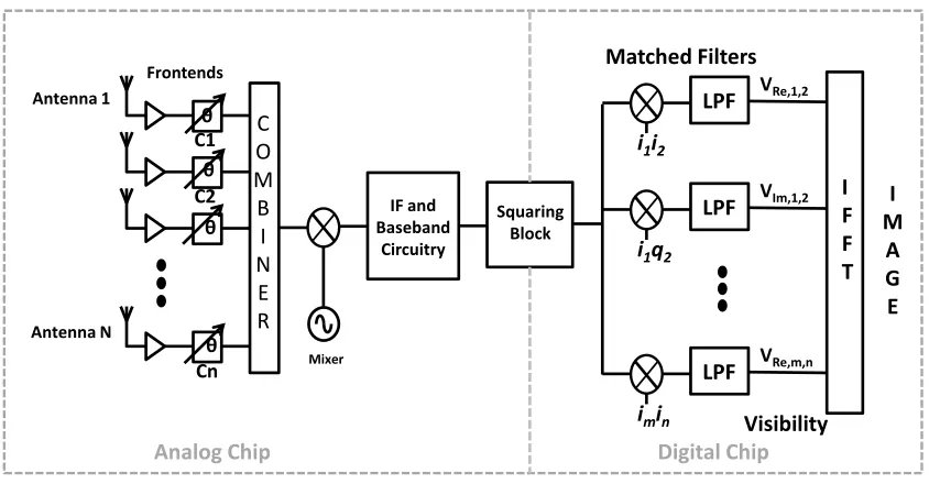
θ θ θ θ C O M B I N E R IF and Baseband Circuitry Mixer Frontends Antenna 1 Antenna N C1 C2 Cn Squaring Block
LPF VRe,1,2
i1i2
LPF VIm,1,2
i1q2
LPF VRe,m,n
imin
Matched Filters I F F T I M A G E Visibility
Analog Chip Digital Chip
such as an analog power detector, an RF mixer, a digital squaring operation, or another
operation which creates an “interference" of the code-multiplexed signal with itself. The
rationale for such a squaring operation is as follows. In a conventional interferometer, the
two signals of interest are correlated or interfered to obtain the visibility products. In Fig. 2.4,
the aggregate code-multiplexed signal is interfered with itself to obtain all possible visibility
products, with the added result that these visibility products are now code modulated
[Flo16; Flo18].
The squared “power" signalp is represented as
p = [ss u m]2=
X
n
|sn|2+2
X
n
inqnsi,nsq,n+2
X
n6=m
(inimsi,nsi,m+qnqmsq,nsq,m+inqmsi,nsq,m).
(2.7)
The squared summation or power signalp includes a summation of all of the “self-powers"
of the individual signals, a summation of the in-phase to quadrature-phase cross-products
of individual signals which are in general orthogonal to one another and would average to
zero, and a summation of all of the code-modulated cross-products between signal pairs.
To demodulate the visibility samples, the power signal is correlated with code products
inim and/orqnqm to obtain the real visibility samples. Likewise, the power signal is
cor-related with code productsinqm to obtain the imaginary visibility samples. Since we are
correlating the square of the summation with a code product, all code products must be
balanced and orthogonal, a property we refer to as “Balanced Orthogonal Code Products"
(BOCP). In general, it is possible to have identical code products occur within a set of
balanced orthogonal codes. This would result in multiple visibility functions obtained at
once or conflicting one with the other. To avoid this, each code product must be balanced
The resulting visibilities obtained are as follows:
vR e,n,m=E(inim .p) =2si,nsi,m (2.8)
vI m,n,m=E(inqm .p) =2si,nsq,m (2.9)
where theE(.)notation is used to denote the expectation or integration function. In the
derivations above, noise has not been included and there will be a component to these
visibilities which relates to the average noise values within the system. Additionally, codes
have been assumed to be perfectly orthogonal; however, code skew can result in partial
cor-relation between codes leading to residues remaining within the demodulated visibilities.
Code modulation has traditionally found use in interferometry in two applications.
Firstly, in phase-switching interferometry[Sul91; Urr99]wherein phase switching is applied
to remove unwanted components (such as, constant total power terms) to obtain
cross-correlations, and secondly in correlator-based interferometers to eliminate small offsets in
correlator outputs that can result from imperfections in circuit operation or from spurious
signals[Tho08]. The technique of multiplying each channel with orthogonal functions and
demodulating with the products of those functions to remove unwanted components is
similar to code-modulated interferometry proposed in this work. However, in this work
the code-modulation and successive demodulation after squaring of combined signal is to
reconfigure a phased array into an interferometer. Code modulation in this application is
primarily to be able to obtain cross-correlations of all pairs of antennas simultaneously.
Removing of unwanted and spurious signals is, however, an added advantage. Overall, CMI
can be seen not just as an extension to, but a different application of a phase-switched
array and presented in detail in Sec. 3.2 for better understanding of extraction of visibilities.
2.3
Balanced-Orthogonal-Code-Products (BOCP)
As discussed in previous section, the proposed approach to code-modulated interferometry
encodes incoming signals using orthogonal codes and decodes desired cross-correlations
or visibilities using balanced-orthogonalcode-products. In particular, the codes must be
chosen such that the product of any two codes from the set is a third unique code – the
code product. Here we discuss the requirements for a code-set to qualify as BOCP with
examples of suitable code sets.
2.3.1
Rademacher Codes
Rademacher codes[Hen64]or divide-by-two codes are inherently balanced, orthogonal,
and BOCP code set. For example, for a code of length eight, the four Rademacher codes are
R0 R1 R2 R3 =
1 1 1 1 1 1 1 1
1 1 1 1 −1 −1 −1 −1
1 1 −1 −1 1 1 −1 −1
1 −1 1 −1 1 −1 1 −1
(2.10)
For a code of lengthL, there are(l o g2L+1)Rademacher codes. The advantage of using Rademacher codes is the ease of generation, where each code can be easily generated using
a frequency divider circuit. The drawback, however, is that the length of the codes increases
exponentially with the total number of code-sets required, or the total number of elements
in the receiver. For smaller number of elements, like in the case of four-element prototype
2.3.2
Hadamard-Walsh Codes
Walsh codes[Wal23]are orthogonal code sets and have been used for the behavioral results
in this section. For a fixed code length, the product of any two codes from a Walsh set gives
a third code from the same set. For example, a complete set of Walsh code for a code of
length eight is:
W0 W1 W2 W3 W4 W5 W6 W7 =
1 1 1 1 1 1 1 1
1 1 1 1 −1 −1 −1 −1
1 1 −1 −1 −1 −1 1 1
1 1 −1 −1 1 1 −1 −1
1 −1 −1 1 1 −1 −1 1
1 −1 −1 1 −1 1 1 −1
1 −1 1 −1 −1 1 −1 1
1 −1 1 −1 1 −1 1 −1
(2.11)
Walsh codes can be generated using Rademacher codes[Hen64], and thus Rademacher
codes can be seen as a subset of Walsh codes. For example, a complete set of Walsh code for
a code of length eight generated using the Rademacher codes isW1=R0,W2=R1,W3=R1R2, W4=R2,W5=R2R3,W6=R1R2R3,W7=R1R3andW8=R3.
It is evident that different code pairs can result in same third code (e.g.,W2W3=W6W7= W4). The BOCP codes used to modulate should be selected such that unique codes are generated by product of any two codes. IfR1,R2 andR3 are used, then only one out of
codes to be able to obtain complex visibility function from all baselines. With increasing
number of antennas, the code length increases significantly and increases the integration
time, reducing the frame rate of the imager. Similar challenge is faced in phase switched
interferometry; more information can be found in[Urr99; Tho08].
2.3.3
Gold Codes
Uncorrelated codes are needed for code-modulated interferometry, where codes are used
to control or modulate each phase shifter in the phased array. Hadamard-Walsh codes or
Rademacher codes are possible candidates as explained in previous section, however, these
codes must be finalized before designing the circuit, limiting system flexibility. Therefore a
more generic code generator is desirable which is software programmable. For this purpose,
Gold codes have been explored in this section because of their bounded correlation property
and easy generation using maximum-length sequences (m-sequences). Gold codes have
only three cross-correlation peaks which reduce in magnitude as the length of the code
increases. Gold codes are also simple to realize through the modulo-2 addition (XOR) of two
m-sequences[Sim94]. In the following paragraphs, we first describe properties and simple
circuits for m-sequence generators and then show how these can be used to generate Gold
codes.
Maximum-length sequences are, by definition, the largest codes that can be generated
using a number of shift registers placed in linear feedback, i.e., linear feedback shift registers
(LFSR). The m-sequence generated by a length of shift registers is decided by the placement
of taps (i.e. XOR gates) in the feedback. For a lengthn of shift registers, the largest code is
of lengthT =2n−1. There can be multiple m-sequences for a given length of shift registers,
Figure 2.5A four stage shift register with one tap generating an m-sequence[Gar10].
Table 2.1Feedback connections for m-sequences[Gar10].
Fig. 2.5 shows a simple block diagram of a four-stage m-sequence generator with the
feedback applied by XORing of the outputs of registers three and four. This is denoted herein
as a tap feedback of[3,4]. Note that for every set of feedback taps, if the tap positions are
“mirrored", an identical sequence reversed in time is generated. For the circuit in Fig. 2.5,
this mirrored sequence is obtained with[4,1]feedback. This concept is easily extendable
to larger sequences, with a summary of the number of registers, feedback locations, and
number of possible m-sequences shown in Table 2.1.
Two m-sequences are used to generate one set of Gold codes as shown in Fig. 2.6. One
m-sequence is delayed and XORed with another to obtain a Gold code. Different Gold codes
of the same set can be obtained by varying the phase delay. Since the two m-sequences
are of same lengthN, all the generated Gold codes of the set are of lengthN. Each pair of
Figure 2.6Two LFSR producing m-sequences Seq 1 and Seq 2 used to generate a Gold code [DJ96].
Fig. 2.6 illustrates a Gold code generation using five-stage m-sequence generators.
Sequence one (Seq1) is programmed to have feedback at[5,3]and Sequence two (Seq2)
is programmed to have feedback at[5,4,3,2]. The length of the m-sequences and Gold
codes=25−1=31; thus, there are 31 Gold codes that can be generated by varying phase shifts in m-sequences. Example sequences are shown below in Table 2.2. Sequence 1 is the
m-sequence for feedback of[5,3]whereas Sequence 2 is the m-sequence for feedback of
[5,4,3,2]. The 0-Shift combination is the Gold code output when Seq1 and Seq2 are XORed
without any phase delay between the two. The 1-Shift combination is the Gold code output
when Seq1 and Seq2 are XORed with a single unit phase delay between the two. Finally, the
30-Shift combination is the Gold code output when Seq1 and Seq2 are XORed with a 30-unit
Table 2.2Gold codes using different sifts[DJ96].
Sequence 1 11111 00011 01110 10100 00100 10110 0 Sequence 2 11111 00100 11000 01011 01010 00111 0
0 Shift combination 00000 00111 10110 11111 01110 10001 0 1 Shift combination 00001 01010 11110 00010 10000 11000 1 30 Shift combination 10000 10001 00010 10001 10001 10101 1
2.4
Behavioral Models
2.4.1
One-dimensional CMI
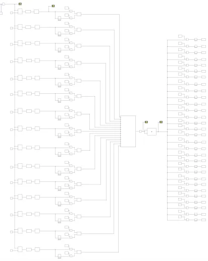
Several behavioral models are created to test the concept using MATLAB®and SIMULINK®. First, conventional interferometry is compared to code-modulated interferometry. Fig. 2.7
shows the block diagram of the behavioral model created to simulate a 1-D CMI. Fig.2.8
shows the behavioural model for an ideal 1-D array of fifteen antennas with wavelength
spacing. To simulate a point source, a wide-band RF noise block is used. To model the path
difference to different antenna elements, a phase shift is applied to the incoming noise
corresponding to the relative geometry of the antennas with respect to the point source. For
example, assuming a parallel wave-front, a wavefront from a point source at 20◦azimuthal
angle would incur a phase difference of 2π.D.s i n(20◦)radian at the two receiving antennas
placed at a distanceD.λapart. As such, fifteen antennas with wavelength spacing receive
the noise signal with a phase shift in multiples of 2π.s i n(20◦)radian, with 1.2π.s i n(20◦)
rad. phase shift for second receiver to 14.2π.s i n(20◦)rad. phase shift for fifteenth receiver.
The signals are then simulated with receiver noise for each element and a band pass
filter to limit the bandwidth, as shown in Fig. 2.9. Each signal is then code-modulated using
Figure 2.7Behavioral model for one-dimensional code-modulated Interferometry.
2.2.2. Hadamard-Walsh codes of length 1024 are used in the simulation which provide 30
BOCP codes. Note that 15 elements require 30 BOCP codes for complex code-modulation,
15 forI and 15 forQcode-modulation, respectively. A MATLAB code is written to select a set
of 30 BOCP codes from a set of 1024 Walsh codes of length 1024, given in Appendix A.1.3. The
code-modulation in a phased array can be achieved using a minimum of 2-bit phase shifter.
All the signals from fifteen receivers are then power combined and squared, as shown in
Fig. 2.10. The squaring operation provides all the cross-correlations (real and imaginary
visibilities) between all possible pairs of antennas. Fig. 2.11 shows the demodulation of
the visibilities from squared signal using matched filters consisting of multiplication with
respective code-products followed by an integration. The visibility samples are then saved
in MATLAB workspace and the data is processed using MATLAB, including the Fourier
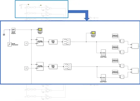
Another SIMULINK model is created to simulate the conventional interferometry for
comparison with CMI. As shown in Fig. 2.12, the conventional interferometry is modeled
using a similar approach; the model consists of a noise source, phase shifts to capture path
length, a noise figure block and bandpass filter to model circuit front end, and a bank of
complex correlators (pairwise multiplication and integration) to obtain complex visibilities.
The visibility samples are once again saved in MATLAB workspace for data processing
including Fourier transform to obtain brightness pattern.
Figure 2.12SIMULINK behavioral model for fifteen elements 1D basic interferometry showing a bank of complex correlators to obtain complex visibility samples.
are compared. The point source consists of a 1-GHz signal with 2-MHz bandwidth to allow
for faster computation. The code modulation applied consisted of a chip rate of 1 MHz with
code length 1024. The results for both interferometers were found to be very similar. Fig. 2.13
shows the plots for one and two point sources at different angles in sky, for conventional
and code-modulated interferometry. Note that CMI imager is able to accurately track
the bright point source, as well as resolve two point sources. These simulations, however,
assume a perfectly cold background with only one or two bright point source(s) emitting
noise-like thermal radiation, and does not included any of the circuit imperfections and
implementation errors. These ideal simulation conditions provide a near-perfect match
in the simulation results of a CMI imager with conventional interferometer. Background
thermal noise, circuit noise, circuit non-linearity, spurious signals, code-skewing, moving
scene, etc. are some of the many imperfections that will affect the actual implementation of
0 20 40 60 80
Angle in Sky (Degrees)
0 0.2 0.4 0.6 0.8 1 Brightness Pattern Traditional Code-Modulated
0 20 40 60 80
Angle in Sky (Degrees)
0 0.2 0.4 0.6 0.8 1 Brightness Pattern Traditional Code-Modulated (a) (b)
0 20 40 60 80
Angle in Sky (Degrees)
0 0.2 0.4 0.6 0.8 1 Brightness Pattern Traditional Code-Modulated
0 20 40 60 80
Angle in Sky (Degrees)
0 0.2 0.4 0.6 0.8 1 Brightness Pattern Traditional Code-Modulated (c) (d)
0 20 40 60 80
Angle in Sky (Degrees)
0 0.2 0.4 0.6 0.8 1 Brightness Pattern Code-Modulated
0 20 40 60 80
Angle in Sky (Degrees)
0 0.2 0.4 0.6 0.8 1 Brightness Pattern Code-Modulated
(e) (f )
Figure 2.13Behavioral modeling results comparing traditional to code-modulated interferome-try: (a)-(d) shows the results of a point source at 20◦, 30◦, 40◦, and 50◦elevation angles; (e) and (f )
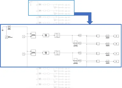
2.4.2
Two-dimensional CMI
To test the code-modulated interferometry for extended sources, the behavioral models
are expanded to a two-dimensional scene and a two-dimensional imaging array. Fig. 2.14
shows the behavioral model for two-dimensional CMI. Extended objects are modeled as
a combination of multiple independent point sources emitting uncorrelated noise. This
makes the object spatially uncorrelated, an important requirement for interferometric
imaging systems. The noise signals then pass through a MATLAB code that models the
shape of object, its distance from imager, and relative path difference of the signals from
different parts of the object to the different receivers in the imaging array1. The MATLAB code to simulate 2-D objects for imaging is given in Appendix A.1.1. The noise sources
are wide-band white-noise block and therefore a band pass filter block is used to limit the
bandwidth, and code-modulation is applied to bothI andQsignal, similar to 1-D CMI. All
of the elements are then power combined and fed into a power detector (squaring). Again,
the results are saved in MATLAB workspace and data is processed in MATLAB, including
the demodulation of the visibilities and the Fourier transform to obtain the image. Twelve
elements are placed in a "T" configuration providing 81 pixels in an image. Fig. 2.15 shows
results for point sources and 2-D "T", "I" and"O" shaped objects and demonstrates the
functionality of the system.
1The phase array imaging toolbox[PT13]provided by TxACE (M. Torlak, UT Dallas) was helpful in
Source Image
2 4 6 8
1 2 3 4 5 6 7 8 9 0.1 0.2 0.3 0.4 0.5 0.6 0.7 0.8
2 4 6 8
1 2 3 4 5 6 7 8 9 0.1 0.2 0.3 0.4 0.5 0.6 0.7 0.8
2 4 6 8
1 2 3 4 5 6 7 8 9 0.1 0.2 0.3 0.4 0.5 0.6 0.7 0.8
2 4 6 8
1 2 3 4 5 6 7 8 9 0.1 0.2 0.3 0.4 0.5 0.6 0.7 0.8
2 4 6 8
1 2 3 4 5 6 7 8 9 0.1 0.2 0.3 0.4 0.5 0.6 0.7 0.8
2 4 6 8
1 2 3 4 5 6 7 8 9 0.1 0.2 0.3 0.4 0.5 0.6 0.7 0.8
2 4 6 8
1 2 3 4 5 6 7 8 9 0.1 0.2 0.3 0.4 0.5 0.6 0.7 0.8
2 4 6 8
1 2 3 4 5 6 7 8 9 0.1 0.2 0.3 0.4 0.5 0.6 0.7 0.8
2.5
Sensitivity Analysis
An important metric for the performance of any radiometer is the sensitivity(∆Tm i n)of the
system, defined as the minimum change in temperature of source that can be detected.
Sensitivity of a single radiometer is given by[Kra86].
∆Tm i n=
KeTs y s
p
∆νH FτL F
, (2.12)
whereKe is sensitivity constant,Ts y s is the system noise (Ts y s =antenna temperatureTA
+receiver noise temperatureTRT),∆νH F is the high-frequency bandwidth andτL F is the
integration time.Ke is a multiplication factor which depends upon different factors such as
the interferometer configuration or phase switching, correlator/power detector,etc.and
can vary between 0.5 and 2p2[Kra86]in radio astronomy for single and pairs of antennas.
In this section we estimate the sensitivity constant (Ke) for an N-element code-modulated
interferometer. The derivation follows the approach similar to as given in book titled Radio
Astronomy by Kraus, Chapter 7, pages 4-22[Kra86].
Let us assume a code-modulated interferometer withN number of elements. To
sim-plify the analysis, let us assume only real visibilities are being obtained. Each element is
connected to an antenna with antenna temperatureTA and each receiver adds a receiver
noise equivalent to noise temperatureTRT. We assume that each element has a frequency
bandwidth of∆νH F centered around a mm-wave frequency ofνH F. Corresponding noise
powers arek TA∆νH F andk TRT∆νH F in each element from background noise and receiver
noise, respectively, wherek is the Boltzmann constant. Noise power in each element given
byk TA1∆νH F,k TRT1∆νH F,k TA2∆νH F,k TRT2∆νH F, ...,k TAN∆νH F,k TRT N∆νH F can be
Ts y sfrom each antenna is thus uncorrelated. A discrete source of temperature∆T produces
a signal power ofk∆T∆νH F in each receiver. TheN elements of the interferometer receive
the correlated signal from the discrete source with different phase shifts due to different
path lengths. Let us also assume that this phase shift isc o sφ1,c o sφ2,c o sφ3, ...c o sφN
for antennas one to N.
Signals fromN elements are code-modulated and power combined using a power
combiner. It is important to note here that all the signals fromN elements are power
combined using a circuit element, such as the Wilkinson power combiner[Wil60]. In a
Wilkinson power combiner, when uncorrelated noise is provided at each of the two input
ports, half of the power from each port is dissipated in the shunt resistor and half of the
power reaches the output port. As such, uncorrelated noise temperatureTs y s1andTs y s2 provide a total noise temperature of(Ts y s1+Ts y s2)/2 at the output port of power combiner. When correlated signals are presented at the input ports of Wilkinson power combiner, the
signals add in power.
At any instant in time, the spectral power of the power combined signal (before the
power detector) for a total power interferometer can be written as (in watts):
W =C0k∆νH F[
X TA+
X TRT +
X
∆T +2∆TXc o sφn] (2.13)
whereC0is a proportionality constant that includes the gains and losses in the receiver. For a code-modulated interferometer, the above equation can be re-written as:
W =C0k∆νH F[
X TA+
X TRT +
X
∆T +2∆TX(±)c o sφn] (2.14)
For anN element CMI, the above equation can be written as:
W =C0k∆νH F[N TA+N TRT+N∆T +2∆T(±1c o sφ1±1c o sφ2±1c o sφ3+...)] (2.15)
or
W =C0k∆νH F[N Ts y s+N∆T +2∆T(±1c o sφ1±1c o sφ2±1c o sφ3+...)] (2.16)
The combined signal is then fed in to a power detector. During demodulation we obtain
a visibility sample, say 2∆T c o sφ1, using the code-products, whereas the d.c. terms such as N Ts y s+N∆T and the other visibility samples 2∆T(c o sφ2+c o sφ3+...)would vanish. This is similar to an N-element phase-switch interferometry, the difference being that in CMI we
use codes to obtain cross-correlations whereas the codes in phase-switch interferometry
are mainly to eliminate system non-idealities. The desired signal power is then given by:
W =C[k∆νH F2∆T c o sφ1]2 (2.17)
whereC is the transfer function of the power detector.
Along with the desired signal, there exists a noise voltage in the power detector output,
originating due to noise-voltage components in the frequency range fromνH F−∆νH F/2 to
νH F +∆νH F/2 beating with each other. This noise voltage has a triangular power spectral
density with close to d.c. maximum of:
Wn o i s e =2C[k N Ts y s]2∆νH F (2.18)
imaged. For extended objects, the total power from the object contributes to the reduction
in the sensitivity. Also, assuming a rectangular passband for the low pass filter (or averaging)
of bandwidth∆νL F, the noise in power detector signal can be written as:
Wn o i s e =2C[k N Ts y s]2∆νH F∆νL F (2.19)
The sensitivity can then be defined as the minimum detectable cross-correlation term
when it is equal to the noise in power detector output,Wm i n =Wn o i s e. Substituting∆νL F =
1/(2τL F), and equating eqns. 2.17 and 2.19, we get:
∆Tv i s=
N Ts y s
p
∆νH FτL F
(2.20)
where∆Tv i s= (2∆T c o sφn)m i n. This is the sensitivity of a single visibility sample. Hence,
for code-modulated interferometry, sensitivity constantKe =N. This degradation of
sensi-tivity is a trade-off to reduce the cost of the imaging system. This reduction in sensisensi-tivity
can be over come by higher bandwidth and longer integration time.
According to[Ruf88], unlike in radio astronomy where the source is relatively smaller
than the FOV, for the extended sources filling the FOV in imaging, the sensitivity is degraded
by the total brightness temperature of the source,i.e. N Ts y sis replaced by (N Ts y s+N∆T) in
the sensitivity equation. Every point in the source contributes to the noise in each visibility
point, and therefore to all the pixels in the image. For a simplified scenario, the sensitivity
of the image is given by[Ruf88]:
∆Ti m a g e=
Ts y s
p Np
p
∆νH FτL F
(2.21)
obtained withN-element phased array andNpnumber of pixels is:
∆Ti m a g e,C M I =
Ts y sN
p Np
p
∆νH FτL F
(2.22)
Sensitivity is also affected by the redundancy in baselines, which is worst for a
zero-redundancy thinned array (Ke =pNp) and improves as the array becomes more filled.
Comparing with the phase-switched interferometry (Ke =2 for two antennas), theKe for
code-modulated interferometry can be up toN due to summation and subtraction ofN
different noise sources. This might seem like a huge reduction in sensitivity but the number
of pixels obtained could be up toN(N−1)per scan as compared to one pixel per scan in
simple interferometer for the same integration time[Ruf88].
As an example, an N-element receiver array with 6-dB noise figure (Ts y s ≈1200 K),
RF bandwidths of 6 GHz and 1 GHz, and a frame rate of 30 Hz,∆Tv i s ≈ 0.08×N and
0.21×N, respectively. The image sensitivity can be further reduced by using redundant
baselines. The code modulation interferometry provides information about all possible
baselines and thus redundant information can also be demodulated and used to average
out receiver noise. For an array withDm i n =λthe FOV isθm a x =±1/2 rad (approx±30◦).
For a 60-GHz system with 6-GHz BW,Dm a x ≈50 mm which gives a resolution of 5.7◦for a
±30◦FOV[Let03]. The resolution can be further improved by dividing the total bandwidth
into narrower bandwidths so that the correlation could be extended over larger baselines.
Reducing the bandwidth would reduce the sensitivity or increase the integration time for
constant sensitivity. This is a trade-off between sensitivity, resolution, and frame rate.
Sensitivity and resolution challenges are inherent to using interferometry for radio
astronomy and even more stringent for imaging, remote sensing and similar applications.
research exists related to interferometry enhancement, including hardware
instrumen-tation, calibration and imaging enhancement algorithms (such as the CLEAN algorithm
[Tho08]). These can be applied as well to code-modulated interferometry.
2.6
Conclusion
In conclusion, with the help of preliminary results from behavioral models and the analysis
for system metrics we presented that the code-modulated interferometry appears to be a
promising and cost-effective alternative to costly imaging systems present in the market
today. One important challenge for code-modulated interferometry is scalability to larger
systems which needs to be investigated and possible improvements to be implemented.
This is the scope of future work. The Walsh BOCP codes place a hard limit on the number of
elements that can be used simultaneously in a CMI imager. A possible solution is to divide
the scene into smaller sectors and use multiple chips. Several different kinds of codes can
be explored, such as m-sequences, Gold codes, complex Walsh codes, or pseudo-random
CHAPTER
3
DEMONSTRATION USING IN-HOUSE
60-GHZ PHASED ARRAY
3.1
Overview
The behavioral models in the previous chapter have successfully demonstrated the
feasi-bility of the proposed code-modulated interferometric imaging system. The behavioral
model has been tested with noise from the circuit but does not include the artifacts such as
![Figure 2.1 Schematic of the measurement of a visibility sample [Sim18].](https://thumb-us.123doks.com/thumbv2/123dok_us/1280746.1160605/23.612.111.514.72.275/figure-schematic-measurement-visibility-sample-sim.webp)


![Figure 2.15 Simulation results for imaging 2-D sources with code modulated interferometricimaging system [Cha16].](https://thumb-us.123doks.com/thumbv2/123dok_us/1280746.1160605/46.612.168.461.90.592/figure-simulation-results-imaging-sources-code-modulated-interferometricimaging.webp)
