8
Single Phase Single Stage Power Factor
Correction Converter with Phase Shift PWM
Technique
G.KAVIARASAN
1, M.G ANAND
21
PG Scholar , Department of Power Electronics and Drives THE KAVERY ENGINEERNG COLLEGE ,salem India. [email protected]
2 Assistant Professor Department of Power Electronics and Drives THE KAVERY ENGINEERNG COLLEGE
,salem India. [email protected]
Abstract— A single-phase, three-level, single-stage power-factor corrected AC/DC converter is presented. that operates
with a single controller to regulate the output voltage. the input inductor act as a boost inductor to have a single stage power factor correction. The outstanding features of the rectifier is that it can produce input currents that do not have dead band regions and an output current that can be continuous when the converter is operating from maximum load to at least half of the load. It can operate with less output inductor current ripple; and the input current has small distortion.
Index Terms— AC–DC power factor correction, phase-shift modulation (PSM), single-stage converters, three-level (TL) converters.
I. INTRODUCTION
Power factor correction (PFC) is very important nowadays for AC-DC power supply to comply with harmonic standards IEC 1000-3-2. By adding passive filters to the rectifier /LC filter input combination , results the converter become very bulky and heavy because of low frequency inductor and capacitor. The single stage power factor corrected converter (SSPFC) provide the features of both power factor pre-regulators and the DC-DC converter cascaded with it. In the two stage AC- DC converters has two stages 1. Rectifying stage 2. Isolation DC-DC conversion stage. AC-DC converter is used for rectifying stage for most of the applications.
The Boost converter shapes the line current so it is almost nearer to sinusoidal. Many methods have been used to remove current harmonics and thus improve the overall system power factor. There are two methods to eliminate or at least reduce the input line current harmonics: one is passive power factor correction (PPFC), and another one is active power factor correction
(APFC). Passive PFC is the simplest and most straight
forward method to eliminate the harmonics of input current. This is achieved by using passive reactive elements either at the input or at the output side of input rectifier employed in the design of AC/DC converter. Advantages of this method are high efficiency, low EMI and simple implementation. However, the main drawbacks particularly at the low frequency the size and weight and also cost.
In active power factor correction switching converters are used to shape the input current drawn by the AC/DC harmonics, smaller converter size due to ability to use high switching frequencies, lighter weight and higher reliability. Active PFC can be implemented by controlling the conduction time of the converter switches to force the AC current to follow the waveform of the applied AC voltage.
Previously proposed single stage AC-DC full bridge converter have the following drawbacks :
1) The current source converter with boost inductor
connected to the input of the full bridge circuit, they lack an energy storage capacitor across the primary side DC bus. It causes the output voltage to have a large low frequency 120-HZ ripple.
2) Some converters have two converter stages and
thus have the cost and complexity associated with two stage converters.
3) Resonant converter that must be controlled using
9
(a)(b)
10
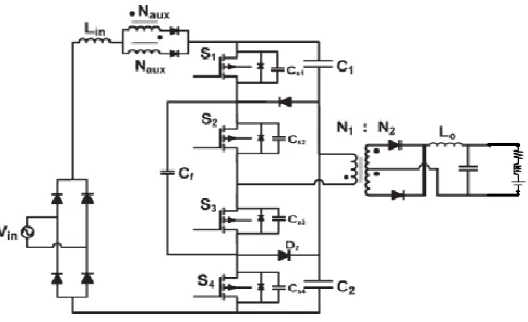
Fig.2.Proposed single-stage three-level converter.II. OPERATION OF THE PROPOSED CONVERTER
The proposed converter is shown in fig 2 it consist of AC input with diode rectifier and three level DC/DC chopper and main power transformer with
auxiliary winding. and the line inductance Lin. The DC
link circuit acts like the Boost switch in an AC-DC PFC boost converter. In previous technique at the same time the two switches should be in on condition so we get
output, if anyone switch get off means the output current will flow to zero.
But in proposed technique if any one switch get off the converter output current will not reach zero the output current will get continuous.
Fig: 3 Waveforms describing the modes of operation. The converter waveform is shown in fig 3,
the converter diagram for different modes is given in fig 4 with the diode rectifier bridge output replaced by a rectified sinusoidal source and thick lines representing the paths of current conduction.
The converter has following modes of operation and it should have 48V DC output for single phase AC supply It should be noted that the DC bus voltage is assumed to be fixed even though the DC bus capacitor
has some ripple due to the 120 Hz component of the diode bridge rectifier output for the purpose of simplicity, as this ripple is negligible compared to the DC component of the bus voltage.
12
(c)(d)
(e)
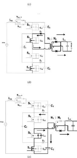
Fig. 4. Modes of operation. (a) Mode 1 (t0 < t < t1). (b) Mode 2 (t 1 < t < t2). (c) Mode 3 (t 2 < t < t3). (d) Mode 4 (t 3 < t < t4). (e) Mode 5(t4 < t < t5)
III-MODES OF OPERATION
1) Mode 1 (t 0 < t < t1) During this mode, MOSFET switches S1 and S2 switches are ON, and the stored energy from DC bus capacitor C1 is transferred to the load. Since the auxiliary winding will generates a voltage (Naux/N1 = 2) that is equal to the total DC-link capacitor voltage (sum of C1 and C2), the voltage across the input
inductor is the rectified supply voltage, and thus, the input inductor current starts rising.
2) Mode 2 (t1 < t < t2): In this mode, S1 is OFF and S2 remains ON. Capacitor Cs1 charges and capacitor Cs4
discharges through Cf, the output capacitance of S4,
13
DC-link capacitors. This mode ends when S4 turns onwith zero-voltage switching (ZVS).
3) Mode 3 (t2 < t < t3): In Mode 3, S1 is OFF and S2 remains ON. The energy stored in the input line inductor during Mode 1 is completely transferred into the DC-link capacitors. The amount of stored energy in the input inductor depends upon the rectified supply voltage. This mode ends when the input inductor current reaches zero. Also, during this mode, the load inductor current freewheels in the secondary of the transformer.
4) Mode 4 (t3 < t < t4) :In this mode, S1 is OFF, the current in the primary of the main transformer circulates through diode D1 and S2, and the load inductor current freewheels in the secondary of the transformer.
5) Mode 5 (t4 < t < t5): In this mode, S1 and S2 are OFF, and the current in the transformer primary charges capacitor C2 through the body diode of S3 and switch S4. This mode ends when switches S3 and S4 are
switched on and a symmetrical period begins. In this mode, the load inductor current continues to transfer energy from the input to the output.
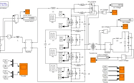
IV- SIMULATION CIRCUIT
14
(a)15
(c)Fig 6 (a) output voltage of the proposed converter.(b) switch voltage Vds3 and (c) switch voltage Vds4 (V : 100 V/div., t: 10 µs/div.).
Fig 6(b),(c) gives the bottom switching voltages of
the switches S3 and S4 under full load condition. The
other switches S1 and S2 have the same voltage
characteristics. The Figure 6(a) shows that the output voltage across the load and switch voltage under different load condition. Here the variation of load from full load to full load, the output voltage is unaltered. The output inductor of the converter can be designed to work in CCM mode over a wide range of load variation and input voltage. Load variations affect the DCM mode of operation. The outstanding features of the rectifier is that it can
produce input currents that do not have dead band regions and an output current that can be continuous when the converter is operating from maximum load. the load used may be resistive load, inductive load, capacitive load or the combination of this. The converter has greater flexibility and ultimately improved performance.
(a)
16
(c)17
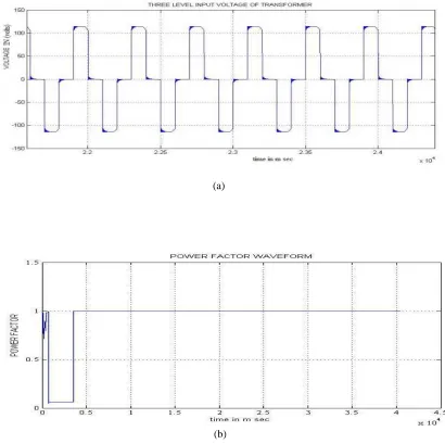
Fig7(a) shows the Simulation result gives theprimary voltage of transformer under full load condition. This is the three level wave form created by the converter. the three level supply voltage is power factor range will very nearer to unity power factor (0.9996 PF), at the initial condition the value (1) that will be given to the switches, in this waveform the top graph plot will be created by switch s1 &s2.
V . EXPERIMENTAL RESULTS
An experimental converter of the
proposed system was built to confirm its feasibility. The converter was designed according to the following specifications
1) Input voltage Vin = 90–265 Vrms 2) Output voltage Vo = 48V 3) Output power Po = 1000W 4) Switching frequency fsw = 50 Hz.
The main switches were FDL100N50F, and the diodes were UF1006DICT. The input inductance is
Lin = 35 µH, Lo = 15 µH and DC-Bus capacitors,
C1 , C2 = 2200 µF. The auxiliary transformer ratio was 1:2 and the main transformer ratio was 2.5:1. VI- CONCLUSION
The purpose of the project was to develop open loop control for the single-stage three level full-bridge converter. A single-phase, three-level,
single-stage power-factor corrected AC/DC
converter that operates with a single controller to regulate the output voltage was presented. This converter has an auxiliary circuit that can cancel the capacitor voltage in which way the input inductor act as a boost inductor to have a single stage power factor correction. The outstanding features of the rectifier is that it can produce input currents that do not have dead band regions and an output current that can be continuous when the converter is operating from maximum load to at least half of the load. The converter can operate with lower peak voltage stresses across the switches and the DC bus capacitors as it is a
three-level converter. This allows for greater flexibility in the design of the converter and ultimately improved performance.
REFERENCES
[1] G. Spiazzi, and F.C. Lee, “Implementation
of single-phase boost power factor
correction circuits in three-phase
applications,” IEEE Trans. On Industrial.
Elec., vol. 44, no. 3, pp 365-371, June
[3] DLiu,ehong Xu, Changsheng Hu, A
High-Efficiency Single-Phase AC/DC
Converter With Enabling Window Control And Active Input Bridge IEEE Trans on
2012.
[4] Majid Pahlevaninezhad, Pritam Das,
Josef Drobnik, Praveen K. Jain and Alireza Bakhshai A ZVS Interleaved Boost AC/DC Converter Used In Plug-In Electric Vehicles” IEEE trans- 2012.
[5] Murray Edington, Wilson Eberle and
William G. Dunford “Control Loop Design For A PFC Boost Converter With Ripple Steering” IEEE-trans- 2013.
[6] “Mehdi Narimani and Gerry
Moschopoulos” A New Single-Phase Single-Stage Three-Level Power-Factor-Correction AC–DC Converter” IEEE
2012.
[7] R. W. Erickson and D. Maksimovic,
Fundamentals of Power Electronics, 2nd ed. Norwell, MA: Kluwer Academic
Publishers, 2001.
[8] Q. Zhao and F. C. Lee, “High-efficiency,
high step-up DC-DC converters,” IEEE
Trans. Power Electron., vol. 18, no. 1, pp. 65–73, Jan. 2003.
[9] C. Y. Inaba, Y. Konishi, and M. Nakaoka,
“High frequency PWM controlled step-up chopper type DC-DC power converters with reduced peak switch voltage stress,” in Proc. IEE Electr. Power Appl., Jan.
2004, vol. 151, no. 1, pp. 47–52.
[10] C. Y. Inaba, Y. Konishi, and M. Nakaoka,
“High frequency PWM controlled step-up chopper type DC-DC power converters with reduced peak switch voltage stress,” in Proc. IEEE Electr. Power Appl., Jan.
18
G.Kaviarasan received
B.E degree from the
Kavery Engineering
College,Salem,Tamilnad
u, India in 2011at
Electrical And
Electronics Engineering. He is a P.G student in the
Department of Power
Electronics And Drives at the Kavery Engineering College
M.G.Anand received B.E
degree from vellalar
College of Engineering,
Erode,Tamilnadu, India
in2007in Electronics and communication
Engineering. He received
P.G degree in the
Department of Power
Electronics And Drives at the KSR College of
technology tamilnadu,