6
DESIGN FOR TESTABILITY I: FROM
FULL SCAN TO PARTIAL SCAN
Chia Yee Ooi
6.1 CONTEXT
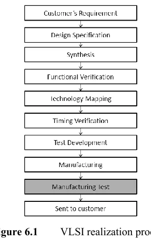
It is important to check whether the manufactured circuit has physical defects or not. Else, the defective part may adversely affect the circuit's functioning. The checking process is called testing or manufacturing test. In other words, manufacturing test is an important step in VLSI realization process. Figure 6.1 shows the process.
As can be seen in Figure 6.1, there is a stage called test development where it basically consists of three activities; test generation, fault simulation and design for testability implementation. Test generation is a method of generating an input sequence that can distinguish between good chip and defective chip when the input sequence (test sequence) is applied to the chip using a tester. Fault simulation is a step of simulating circuits in the presence of faults. This step is used to evaluate the quality of a set of test sequence by indicating the fault coverage of the test sequence applied to a circuit. Fault simulation is used to generate a minimal set of test sequence as well. Note that test generation and fault simulation are done prior to fabrication. Besides, design for testability (DFT) is also considered before manufacturing process. DFT is a method that augments a circuit so that it is testable.
Figure 6.1 VLSI realization process.
fault model is first determined. Stuck-at fault model is still commonly used as a fault model because it can mimic many manufacturing defects. The following section evaluates general fault models and stuck-at fault model.
6.2 FAULT MODELS
Fault modeling alleviates the test generation complexity because it obviates the need for deriving tests for each possible defect. In fact, many physical defects map to a single fault at the higher level. Therefore fault modeling is essential in testing. This section introduces fault models at logical level. These fault models include single stuck-at fault model, multiple stuck-at fault model, path delay fault model and segment delay fault model.
technology. Furthermore, it has empirically shown that tests that detect single stuck-at faults detect many other faults as well. In structural testing, it is necessary to make sure that the interconnections in the given circuit are able to carry both logic 0 and 1 signals. The stuck-at-fault model is derived directly from these requirements. A line is stuck-at 0 (SA0) or stuck-at 1 (SA1) if the line remains fixed at a low or high voltage level, respectively. A single stuck-at-fault that belongs to the single stuck-at-fault model is only assumed to happen on only one line in the circuit. If the circuit has k lines, it can have 2k single SAFs, two for each line.
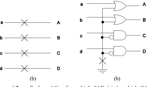
If the stuck-at-fault occurs on more than one line in the circuit, the faults are said to belong to the multiple stuck-at-fault model. To model a circuit with a multiple stuck-at-fault by a model containing only one single stuck-at fault, m extra gates are added into the circuit as follows, where m is the multiplicity of faults.
A two-input OR (resp. AND) gate is inserted in a line if the line is stuck-at 1, SA1 (resp. stuck-at 0, SA0) and one of the input lines of the gate is fed from the ground of the circuit as a fanout branch of a ground line G. The input of AND gate that is fed from line G is inverted. The multiple fault is then represented by a single SA1 fault on the fanout stem G.
The controlling value of each gate is the same as the value at which the line is stuck. Thus, the faulty value appears on the output of each gate if the SA1 fault on line G is activated. Otherwise, the gate forces the correct value on it. Thus, the model is satisfying the conditions of circuit equivalence and fault equivalence.
(b) (b)
Figure 6.2 Fault modeling for multiple SAF. (a) A multiple SAF. (b) An equivalent single SAF.
6.3 TEST GENERATION MODELS
equivalent or one order greater than that of combinational circuits have started.
6.3.1 Time Expansion Model
Time expansion model has been widely used as an approach of test generation of acyclic sequential circuits as the tests can be generated by applying combinational test generation to the time expansion model.
Definition 6.1 A topology graph is a directed graph G = (V, A, r) where a vertex v V denotes a combinational logic block which contains primary inputs/outputs and logic gates, and an arc (u, v) A denotes a connection or a bus from u to v. Each arc has a label r : A → Z+ (Z+ denotes a set of non-negative integers), and r(u, v) represents the number of registers on a connection (u, v).
Definition 6.2 Let SA be an acyclic sequential circuit and let G = (V, A ,r) be the topology graph of SA. Let E = (VE, AE, t, l) be a directed graph, where VE is a set of vertices, AE is a set of arcs, t is a mapping from VE to a set of integers, and l is a mapping from VE to a set of vertices V in G. If graph E satisfies the following four conditions, graph E is said to be a time expansion graph (TEG) of G.
C1 (Logic block preservation): The mapping l is surjective, i.e., v V, u VE s.t. v = l(u).
C2 (Input preservation): Let u be a vertex in E. For any direct predecessor v pre( l(u) ) of l(u) in G, there exists a vertex u in E such that l(u') = v and u' pre(u). Here, pre(v) denotes the set of direct predecessors of v.
C3 (Time consistency): For any arc (u, v) AE, there exists an arc ( l(u), l(v) ) such that t(v) - t(u) = r( l(u), l(v) ).
Definition 6.3 Let SA be an acyclic sequential circuit, let G = (V, A, r) be the topology graph of SA, and let E=( VE, AE, t, l) be a TEG of G. The combinational circuit CE(SA) obtained by the following procedure is said to be the time expansion model (TEM) of SA based on E.
1. For each vertex u VE, let logic block l(u) V be the logic block corresponding to u.
2. For each arc (u, v) AE, connect the output of u to the input of v with a bus in the same way as ( l(u), l(v) ) A). Note that the connection corresponding to (u, v) has no register even if the connection corresponding to ( l(u), l(v) ) has a register (i.e. r( l(u), l(v) ) > 0).
3. For a line or a logic gate in each logic block obtained by Step (1) and (2), if it is not reachable to any input of other logic blocks, then it is removed.
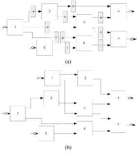
Figure 6.3(b) shows a TEM, which is the test generation model for the sequential circuit called S1 in Figure 6.3(a). Rectangulars labeled from 1 to 7 are combinational blocks while the highlighted ones are registers. Inputs x10 and x11 of the TEM are derived from input x1 of
S1. Similarly, combinational blocks labeled 1 and 2 are duplicated based on the definition of TEM.
6.4 DESIGN FOR TESTABILITY
Generally, the test generation problem of a sequential circuit is modeled by an iterative logic array that consists of several time frames so that it can be solved by combinational test generation techniques. The model is shown in Figure 6.4. The test generation problem involves the following three steps.
(a)
(b)
Figure 6.3 Time expansion model. (a) An acyclic sequential circuit S1. (b) Time expansion model for S1.
Figure 6.4 Iterative logic array model.
differentiation fails, step 1 is performed again to get a different excitation state for state justification and state differentiation. Logic duplication of the combinational part takes place at every time frame for state justification and state differentiation. In the worst case, i and
j equal 2p, where p is the number of memory elements. These factors result in high complexity for test generation of cyclic sequential circuits.
Design for testability (DFT) is a method of augmenting a sequential circuit so that it becomes more easily testable. When it becomes more easily testable, its test generation problem can be modeled by other representation like combinational test generation model or time expansion model (TEM). In this section, we discuss several techniques of DFT such as full scan and partial scan techniques.
6.4.1 Full Scan Technique
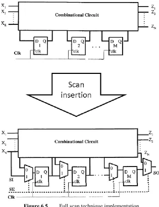
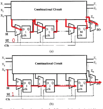
Test generation problem for sequential circuits is more complex mainly due to the feedback formed by the sequential elements such as flip-flops and registers. In other words, the controllability and observabilty of some flip-flops and registers are very poor. Full scan technique has been introduced to resolve this problem. Full scan technique is to connect all the flip-flops (or registers) to form a shift register by augmenting each flip-flop into a scan flip-flop. A scan flip-flop consists of a normal flip-flop and a multiplexer.
After augmentation, there is an additional input that selects the operation mode of the circuit. In the circuit shown in Figure 6.5, the circuit is in normal operation mode if input SE = 0 where the outputs of the combinational circuit are fed back to the inputs of the circuit through the flip-flops. When SE = 1, the flip-flops act as a shift
register. This is illustrated in Figure 6.6.
However, full scan technique has a drawback. The additional multiplexers in the full scan design circuit result in large area overhead. Therefore, partial scan techniques have been introduced to overcome the drawback.
(a)
(b)
6.4.2 Partial Scan Techniques
Several partial scan techniques have been introduced to overcome the large area overhead resulted in full scan design. Whereas full scan design circuit has a kernel which consists of purely combinational circuit, partial scan design circuit has a kernel which is an acyclic sequential circuit (Gupta and Breuer, 1992). There are some classes of acyclic sequential circuit which can be the kernel of partial scan design circuit. The test generation complexity for acyclic sequential circuits is proved to be one order greater than combinational test generation complexity.
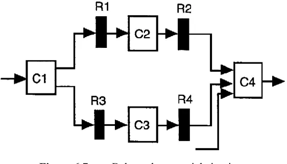
6.4.1.1 Balanced Sequential Circuits
(Gupta and Breuer, 1990) Let a directed graph G = (V, A, H)
represents a sequential circuit. The set V of vertices represents a set of clouds where each cloud is a maximal region of connected combinational logic such that its inputs are either primary inputs or outputs of registers and its outputs are either primary outputs or inputs to registers. The set A of arcs represents a set of connections between two clouds through a register. Arcs in H A represent HOLD registers. A sequential circuit is said to be a balanced sequential circuit if
1. G is acyclic
2. vi, vj V, all directed paths (if any) from vi to vj are of equal length
3. h H, if h is removed from G, the resulting graph is disconnected.
The example balanced sequential circuit is as shown in Figure 6.7.
6.4.1.2 Strongly Balanced Sequential Circuits
Figure 6.7 Balanced sequential circuits.
each cloud is a maximal region of connected combinational logic such that its inputs are either primary inputs or outputs of registers and its outputs are either primary outputs or inputs to registers. A
represents a set of connections between two clouds. A weight, w(a)
on the arc a = (vi, vj) equals to the number of registers between the corresponding clouds. A sequential circuit is a strongly balanced sequential circuit when the following conditions are satisfied
1. G is acyclic
2. vi, vj V, all directed paths (if any) from vi to vj are of equal length
3. there exists a function t from v to a set of integers such that
t(vi) = t(vj) + w(a) for a =( vi, vj).
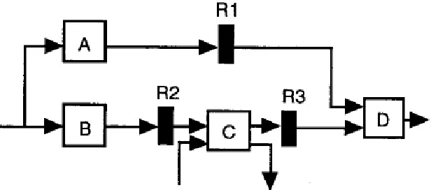
6.4.1.3 Internally Balanced Sequential Circuits
-transformation. Suppose x is a primary input and xi and xj are branches of x. If no path exists such that a primary output zk can be reached from xi and xj over equal depth paths, then xi and xj are called separable. Equal depth paths are the paths where the number of flip-flops included in each of the paths is the same. C*-transformation consists of the following two operations
1. For a primary input with fanout branches, the set of fanout branches of that primary input is denoted by X. Let us obtain the smallest partition of X which satisfies the following statement: If branches xi and xj belong to different blocks X(i), X(j) of partition Π( xi X(i), xj X(j), X(i) ≠ X(j) ), then xi and xj are separable. Each partitioned block is provided with a new primary input separated from the original primary input 2. All flip-flops are replaced by wires.
The example for internally balanced sequential circuit is shown in Figure 6.8.
Partial scan technique can be defined based on the structure of the resulting kernel of the modified circuit. Partial scan technique select a subset of flip-flops to be converted to scan flip-flops so that the kernel of the circuit become balanced sequential circuit, strongly
balanced sequential circuit, internally balanced sequential circuit or acyclic sequential circuit.
6.5 ADVANCED PARTIAL SCAN TECHNIQUE: D-SCAN
TECHNIQUE
In order to further reduce the hardware area overhead, the number of flip-flops to be converted into scan flip-flops should be reduced. To achieve the objective, several partial scan techniques have been introduced. The partial scan technique, which breaks the minimum feedback loops (Lee and Reddy, 1990), succeeds in reducing the number of scan flip-flops. This is then further reduced by cost-free scan (Lin et al., 1998) that establishes paths in the scan chain using existing logic and thus reduces the area overhead. Orthogonal scan (Norwood and McCluskey, 1996) and partially strong testability method (Iwata et al., 2005) are among other scan techniques but they are applicable in datapath only. Besides DFT method, some works have introduced synthesis-for-testability (SFT) methods to augment a given design into easily testable based on the information obtained at high-level description (Abadir and Breuer, 1985; Agrawal and Cheng, 1990; Kanjilal, Chakradhar and Agrawal; Fujiwara et al., 1975).
which the existing paths are dependent to enable the signals transfer through the paths. This information can be obtained from the behavioral description of a design. Therefore, extra gates are not needed to enable the signals transfer for some existing paths. This can reduce the area overhead of the augmented circuit. D-scan technique can be applied to any sequential circuit at gate-level and RT-level.
From different viewpoint, D-scan does not differentiate controller unit from datapath unit when identifying scan flip-flops. The signal transfer along a scan path (Path A) is enabled by an existing signal which may come from another scan path (Path B). If the signal is needed to enable the signal transfer on Path A and is being transferred along Path B simultaneously, we call the situation as path dependency. Our method has to resolve path dependency despite of lower area overhead. This can be done through activating hold function of flip-flops.
6.5.1 Thru Function
This sub-section defines thru function, which is a logic function that allows signal transfer from its input to its output.
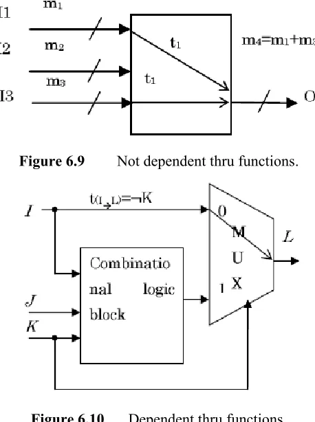
Definition 6.4 Thru function t is a logic that transfers the signals from the input of the thru function to the output. The output signals are the same with the input signals if the thru function is active. Note that the bit width of the input and output are equal.
Two thru functions are independent if they cannot be active at the same time. t1 and t2 in Figure 6.9 are independent. Note that the multiplexing logic in a scan flip-flop is a kind of thru functions. Two thru functions ti→j and tl→m are said to be dependent if they cannot be active at the same time.
at the same time. Figure 6.10 illustrates another example circuit that consists of three multiplexers. Thru function ti→o=p q and thru function tk→o = pq are dependent as shown by the Boolean formula in each thru function.
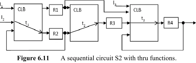
When a series of thru functions form a tree (or path), then it's called a scan path or a scan tree. For example, path I2 → R2 → R3 → R4 in Figure 6.11 is a scan path.
6.5.2 R-Graph
We also introduce a circuit representation called R-graph. R-graph
Figure 6.9 Not dependent thru functions.
Figure 6.11 A sequential circuit S2 with thru functions.
contains the information of circuit connectivity, thru functions, and signals that activate the thru functions.
Definition 6.5 A circuit representation called R-graph is a directed graph G = (V, A, w, r, t) that has the following properties.
1. Let FFi denotes a flip-flop. Let pre(FFi) = {FFj|FFj C FFi} ( resp. suc(FFi) = {FFj|FFi C FFj} ) where c is a combinational path. v V is a primary input or primary output or register that consists of a maximal set of flip-flops such that pre(FFp) = pre(FFq) and suc(FFp) = suc(FFq) for all FFp, FFq in the set of flip-flops.
2. (vi, vj) A denotes an arc if there exists a combinational path from the register corresponding to vi to the register corresponding to vj.
3. w: V → Z+ (the set of positive integers) defines the number of flip-flops in each register corresponding to a vertex.
4. r: V → {h, } defines type of a register where the register is a hold register v if r(v) = h. Else, it is a regular register. Note that r(w) = if w corresponds to a primary input or primary output.
values are transferred from u to v through a wire logic (not a gate logic) directly. Note that identity thru function is always active.
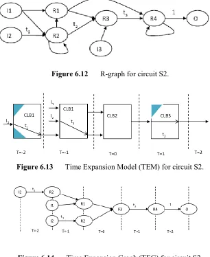
Figure 6.12 shows the R-graph of the sequential circuit S2 of Figure 6.11. The notation CLB in Figure 6.11 means combinational logic block. The thru functions t1 – t3, which are the thru functions extracted from the high level netlist of S2, are contained in the R-graph. t3 = R1 means thru function t3 is activated by signal value 1 at register R1.
To generate test patterns for a CLB in a sequential circuit with our DFT method, we use time expansion model (TEM), which is similar to the case of partial scan design. Figure 6.13 shows the TEM for S2. It can be represented in R-graph as shown in Figure 6.14. TEM is the better model because we can see explicitly the connectivity between registers, inputs and outputs. For instance, there is no connection between I2 and R1 but it is not visible in Figure 6.13. The highlighted triangle parts mean unused logic parts when the circuit is transformed into TEM for test generation purpose.
6.5.3 Types of Path Dependency
When a signal of an input or an output of a register is used to activate a thru function and to justify any other signal simultaneously in testing mode, this may degrade the fault coverage because the signal is more flexible to justify the other signal in the normal operation mode where activating a thru function is not considered. This situation is called path dependency.
Figure 6.12 R-graph for circuit S2.
Figure 6.13 Time Expansion Model (TEM) for circuit S2.
Figure 6.14 Time Expansion Graph (TEG) for circuit S2.
1. Active-normal dependency – there exists an input or a register output that activates a thru function and justifies any other signal line simultaneously.
2. Thru-normal dependency – there exists an input or a register output that transfers a data along a scan path (or scan tree) and justifies any other signal line simultaneously.
output that activates a thru function of a scan path and transfers a data along another scan path simultaneously. 4. Active-active dependency – there exists an input or a register
output that activates two different thru functions with different logical values.
Figure 6.15 shows these four different types of dependency in R-graphs. Note that the dependency can occur for more than two edges as shown in Figure 6.15(e).
To resolve a path dependency, hold function is used. A subset of the destination vertices need to be in hold mode in order to resolve a path dependency. We will use time expansion model in R-graph to explain the method for each type of path dependency. Note that in Figure 6.16, when the register represented by Node 2 in the graph is put in the hold mode to hold a signal value for time frames t1 and t2, signal from Node 1 is no more needed simultaneously for two purposes (thru function activation and data transfer, thru function and normal justification, etc.) and thus the path dependency is resolved.
6.6 D-SCAN ALGORITHM
This section describes a design for testability (DFT) method to augment a given sequential circuit using D-scan technique (Ooi and Fujiwara, 2006). The DFT method performs some operations on R-graph and it is designed to induce minimum area overhead. The procedure consists of the following five steps.
Step 1 Identify the vertices of minimum feedback vertex set (MFVS).
Step 2 Identify existing thru trees.
Step 3 Group the vertices of MFVS into three groups G1, G2 and G3 as follows.
(a) (b)
(c) (d)
(e)
Figure 6.15 Types of path dependency. (a) Active-Normal dependency. (b) Thru-Normal dependency. (c) Active-Thru dependency. (d) Active-Active dependency. (e) Multi-edge dependency.
vertex is in an existing thru tree Ti, group all the vertices in Ti in G1. If G1 has only input/output, G1 is made empty.
3.2 Group the remaining register vertices in MFVS into G2.
(a) (b)
(b) (d)
(e)
Figure 6.16 Resolution of path dependency. (a) Active-Normal dependency. (b) Thru-Normal dependency. (c) Active-Thru dependency. (d) Active-Active dependency. (e) Multi-edge dependency.
Step 4 For each group of G1 and G2, the following is done.
input vertex (resp. output vertex), one input vertex (resp. output vertex) is taken from G3. If G3 does not have one, a new vertex is added into the group.
4.2 Group each vertex (except output vertex) into a group called potential source if the vertex does not have an outgoing arc labeled with a thru function.
4.3 Group each vertex (except input vertex) into a group called potential destination if the register vertex does not have an incoming arc labeled with a thru function. 4.4 For each vertex u in the group of potential source,
introduce a new outgoing arc labeled with a new thru function tnew to connect u to a vertex v in the group of potential destination. u and v are taken out from the groups of potential sources and potential destination, respectively.
4.5 Repeat 4.4 until the group of potential destination is empty or the group of potential destination has only output vertices.
4.6 For each vertex u in the group of potential source, introduce a new outgoing arc labeled with a new thru function tnew to connect u to an output vertex v that does not have an incoming arc labeled with thru functions. If the group does not have one, an output vertex is taken from G3 to the group. If G3 does not have one, a new output vertex is introduced to the group.
Step 5 If G1 is not empty, each register in G1 and G2 is augmented into a hold register. For other register vertices in MFVS, each register is augmented into a register with reset function.
new primary input.
6.7 CASE STUDIES
In the case studies (Ooi and Fujiwara, 2006), experiments are conducted on RTL benchmark circuits, which are datapaths of varying bit width. Our DFT method is applied on the datapaths of GCD, LWF, JWF, and MPEG and the area overhead of the augmented circuits are compared with that of the full scanned circuits and the partial scanned circuits. Partial scanned circuits are the circuits whose minimum feedback set of flip-flops are scanned so that the augmented circuits are acyclic. Thus, the circuits modified with partial scan and with our DFT method have same test generation complexity. Table 6.1 presents the characteristics of the benchmark circuit. Table 6.2 shows the fault coverage and fault efficiency of each benchmark circuit. Each fault testable in the partial scan designed circuits is also testable in the corresponding circuit augmented by our DFT method, and vice versa. Table 6.3 shows the area overhead where one unit of area corresponds to the size of an inverter and pin overhead. It shows that the area overhead of the benchmark circuits augmented by our method is less than that of the full scanned circuits and the partial scanned circuits. Table 6.4 tells that the test generation time for the original circuits is large while the test generation time for the partial scan designed circuits as well as the acyclically testable sequential circuits is small. Table 6.5 also gives the information that the test application time of the circuits under our augmentation is more than the original circuits' but less than the partial scan.
Table 6.1 Benchmark circuit characteristics
Benchmark Original
# Flip-flops Area # Primary inputs # Primary outputs
GCD 48 1,383 40 19
LWF 80 1,763 39 32
JWF 224 5,925 106 80
Table 6.2 Number of faults, fault efficiency and fault coverage
Benchmark Original Full/Partial scan Our method
FC (%) FE (%) FC (%) FE (%) FC (%) FE (%)
GCD 99.75 99.75 100 100 100 100
LWF 99.94 99.94 100 100 100 100
JWF 98.70 98.70 100 100 100 100
MPEG 84.80 84.80 100 100 100 100
Table 6.3 Area overhead (1 unit=size of NOT gate)
Benchmark Full scan Partial scan Our method
GCD 1,719 (24.30) 1,495 (8.10) 1,415 (2.31)
LWF 2,323 (31.76) 1,875 (6.36) 1,798 (1.99)
JWF 7,493 (26.46) 6,485 (9.45) 5,957 (0.54)
MPEG 60,268 (28.85) 47,612 (1.80) 47,556 (1.68)
Table 6.4 Test generation time (s)
Benchmark Original Full scan Partial scan Our method
GCD 87.19 0.02 0.19 0.43
LWF 49.02 0.02 0.06 0.40
JWF 1,689.14 0.08 0.50 13.48
MPEG 2,646.42 0.18 12.05 33.91
Table 6.5 Test application time (clock cycles) Benchmark Original Full scan Partial scan Our method
GCD 159 6,124 3,334 815
LWF 59 4,049 1,444 196
JWF 103 17,100 12,488 1,648
MPEG 114 162,035 31,822 9,690
6.8 CHAPTER SUMMARY
circuit with acyclic sequential circuit kernel which is more easily testable. Experimental results showed that the area overhead of the resulting augmented circuits is less compared to the partial scan designed circuits. Complete fault efficiency is also achieved and the test generation time is low. Moreover, the test application time is less than the test application time of the full scanned circuits and partial scanned circuits.
REFERENCES
Abadir, M. S. and M. A. Breuer. (1985). A knowledge based system for designing testable VLSI chips. IEEE Design and Test of Computers. 2(4):56-68.
Agrawal, V. D. and K. T. Cheng. (1990). Finite state machine synthesis with embedded test function. Journal Electronic Testing: Theory and Applications. 1(3):221-228.
Asaka, T., S. Bhattacharya, S. Dey and M. Yoshida. (1997). H-Scan+: a practical low-overhead RTL design-for-testability technique for industrial designs. Proc. Int. Test Conf. :265-274.
Balakrishnan, A. and S. T. Chakradhar. (1996). Sequential circuits with combinational test generation complexity. Proc. IEEE Int. Conf. VLSI Design. :111-117.
Bhattacharya, S. and S. Dey. (1996). H-Scan: a high level alternative to full-scan testing with reduced area and test application overheads. Proc. IEEE 14th VLSI Test Symp. :74-80.
Chakradhar, S. T., A. Balakrishnan and V. D. Agrawal. (1995). An exact algorithm for selecting partial scan flip-flops. Journal Electronic Testing: Theory and Applications. :83-93.
Fujiwara, H. (2000). A new class of sequential circuits with combinational test generation complexity. IEEE Trans. on Computers. 49(9):895-905.
testable sequential machines with extra inputs. IEEE Trans. on Computers. C-24(8):821-826.
Fujiwara, H. and S. Toida. (1982). The complexity of fault detection: an approach to design for testability. Proc. 12th Int. Symp. on Fault Tolerant Computing. :101-108.
Gizdarski, E. and H. Fujiwara. (2002). SPIRIT: A highly robust combinational test generation algorithm. IEEE Trans. Computer-Aided Design of Integrated Circuit and Systems. 21(12):1446-1458.
Goel, P. (1980). Test generation cost analysis and projections. Proc.
17th DAC.:77-84.
Gupta, R. and M. A. Breuer. (1990). The BALLAST methodology for structured partial scan design. IEEE Trans. on Computers. C-39(4):538-544.
Gupta, R. and M. A. Breuer. (1992). Testability properties of acyclic structures and applications to partial scan design. Proc. IEEE VLSI Test Symp. :49-54.
Inoue, T. et al. (1998). An optimal time expansion model based on combinational ATPG for RTL circuits. Proc. 7th ATS. :190-197.
Iwata, H., T. Yoneda, S. Ohtake and H. Fujiwara. (2005). A DFT method for RTL data paths based on partially strong testability to guarantee complete fault efficiency. Proc. IEEE 14th Asian Test Symp. :306-311.
Kanjilal, S., S. T. Chakradhar and V. D. Agrawal (1995). Test function embedding algorithms with application to interconnected finite state machines, IEEE Trans. CAD. 14:1115-1127.
Lee, D. H. and S. M. Reddy. (1990). On determining scan flip-flops in partial-scan designs. Proc. Int. Conf. on Computer-Aided Design. :322-325.
overhead scan for data paths. Proc. Int. Test Conf. :659-668. Ooi, C. Y. and H. Fujiwara. (2006). A new class of sequential circuits
with acyclic test generation complexity. Proc. 24th IEEE ICCD. :pp. 425-431.
Prasad, M. R., P. Chong and K. Keutzer. (1999). Why is ATPG easy?