Available online:
https://edupediapublications.org/journals/index.php/IJR/
P a g e | 1434Closed Loop Control of Renewable Source Fed
Asymmetrical PWM Full Bridge Converter
V.Jagadeesh M-tech Student Scholar
Department of Electrical & Electronics Engineering, VITAM College of Engineering, sontyam;
Visakhapatnam (Dt); A.P, India.
Y. Naveen Kumar Assistant Professor
Department of Electrical & Electronics Engineering, VITAM College of Engineering, sontyam;
Visakhapatnam (Dt); A.P, India. Abstract- This paper presented a closed loop control of
asymmetrical PWM full bridge converter; Renewable energy and distributed generation are getting more and more popular, wind turbines, and fuel cells. The renewable energy sources need the power electronics interface to the utility grid because of different characteristics between the sources and the grid. No matter what renewable energy source is utilized, extended voltage and power output, less maintenance and higher fault tolerance, the asymmetrical PWM full bridge converter are good, for utility interface of various renewable energy sources. This dissertation proposes a new PWM converter topology and control scheme. Compared to traditional converter, they have enhanced system reliability to no shoot-through problems and lower switching loss with the help of using power closed loop control. The closed loop control, it theoretically eliminates the inherent current zero-crossing distortion of the single-unit asymmetrical type PWM full bridge converter. In addition, the closed loop control can greatly reduce the ripple current or cut down the size of passive components by increasing the equivalent switching frequency. An asymmetrical full bridge PWM technique is proposed for closed loop control of renewable energy sources. The proposed approach is to cut down the switching loss of power control. At the same time, this PWM full bridge leads to current ripple reduction, and thus reducing ripple-related loss in filter components. PWM with feedback controlling is employed for the voltage control of the system. A power management system is designed for the proposed system to manage power flow among different sources.
Index Terms—Asymmetrical pulse-width modulated (PWM), full-bridge converter, soft switching, Closed Loop Controller, PV System.
I. INTRODUCTION
An asymmetrical full bridge boost DC/DC switching converter is proposed to improve renewable systems. Such a new step-up power converter in a PV system provides a low input current ripple injected into the photovoltaic generator, and at the same time provides a low voltage ripple to the load [1-2]. Low-ripple and high boosting conditions make this converter an ideal candidate for photovoltaic systems design, in particular for grid-connected applications. The converter circuitry is analyzed, and a design procedure is proposed in terms of
typical photovoltaic systems requirements [3-5]. Photovoltaic power systems are efficient alternatives to provide electrical energy providing redundancy for critical applications, energy generation, and the reduction of traditional energy generation that impacts the environment. Similarly, photovoltaic generators have been intensively used in residential applications and autonomous and portable applications. Photovoltaic systems require a power electronics interface to define their operating point at optimal conditions for any load. For that DC/DC and DC/AC converters are widely used [6-8]. The double-stage approach is widely accepted due to its application in distributed generation system based on multiple generators, as well as in stand-alone DC applications, where a single DC/DC converter is required [9-10].
The PV applications commonly adopt boosting converters for grid-connected applications due to the requirement of increasing the voltage to the grid connected inverter operating conditions. Other characteristics required in PV applications are a low current ripple injected to the PV and high conversion efficiency [11]. The current ripple magnitude is an important factor in the selection of power converters for PV applications because high current ripples produce an oscillation around the maximum power point (MPP) that reduces the energy extracted from the PV generator. So that most commonly employed converter is boost converter, but in such a boost converter, the current ripples injected to the PV generators depend on the inductor size, switching frequency, input capacitor, and high frequency power source impedance; therefore, in order to reduce the current ripple, it is necessary to increase the converter inductance or input capacitance [12-14]. This can be addressed by using an additional filter between the PV generator and the power converter, also increasing power losses, size, weight, cost, and the order of the system.
II. PHOTOVOLTAIC SYSTEM
Available online:
https://edupediapublications.org/journals/index.php/IJR/
P a g e | 1435photovoltaic effect. Photovoltaic power generation employs solar panels composed of a number of solar cells containing a photovoltaic material. Materials now used for photovoltaic system include mono crystalline silicon, cadmium telluride, poly crystalline silicon and amorphous silicon. Due to the increased demand for different renewable energy sources, the manufacturing of solar cells and photovoltaic arrays has advanced considerably in recent years.
Fig.1. Generally block diagram of proposed DC-DC APWM full bridge Converter with Closed Loop.
(PV) cells are environmentally friendly once they are made but have some other drawbacks. They produce a low voltage that is not compatible with the electric grid and common appliances. This means that the power must be converted into a higher voltage and then inverted to an AC voltage. Also, the PV voltage is prone to fluctuations due to variables like shading and angle of the sun. One method used to produce a large DC voltage from PV modules is to put several in series. The power from the PV modules are put directly into a DC-AC inverter. This system does not require a DC-DC converter that is the power loss to this part of the system does not exist. There are however several large drawbacks. If there is any shading occurs on any of the PV modules the voltage will drop across the whole system and will possibly make the power produced by the rest of the modules unusable. This system also limits the control of the DC voltage going into the DC-AC inverter again putting limits to when the power from the PV can be used. Another method used is to dedicate a DC-DC converter and a AC-DC inverter [2] to each module. The power from the PV module is directed into a DC-DC converter that has high gain capabilities and then to a DC bus. It is then send to a DC-AC inverter and then to the grid or a load. This method makes shading less of an issue as each module has its own DC-DC converter. This however introduces new sources of power loss to the system. The DCDC converter is also
required to produce a large gain which can put strain on its components and also make the converter less efficient
III ANALYSIS OF A PWM FULL-BRIDGE CONVERTER
A. Circuit Configuration and Operation Principle A circuit configuration of the highly efficient APWM full bridge converter for low input voltage range is shown in Fig.2. The configuration of the proposed converter is basically similar to that of the conventional full-bridge converter except for the dc blocking capacitor and the secondary side of the transformer. The primary side of the transformer consists of the primary winding turns Np, the four switches, and the dc blocking capacitor
Cb. The secondary side has the secondary winding Ns, the output diode Do, and the output capacitor Co.
Fig.2.Circuit diagram of the proposed APWM full-bridge converter.
To analyze the steady-state operation of the proposed APWM full-bridge converter, the following assumptions are made.
1) The transformer is modeled as an ideal transformer with the primary winding turns Np, the secondary winding turns Ns, the magnetizing inductance Lm, and the leakage inductance Llk 2) All switches S1–S4 are considered as ideal
switches except for their body diodes and output capacitors (CS1=CS2=CS3=CS4= Coss).
3) The dc blocking capacitor Cb and the output capacitor Co are large enough to neglect the voltage ripple on it, so the voltages across Cb and
Co are constant.
Available online:
https://edupediapublications.org/journals/index.php/IJR/
P a g e | 1436Mode 1 [t0, t1]: At t0, the switches S2 and S3 are turned off. The primary current ip discharges the output capacitances CS1 and CS4 of the switches S1 and S4 and charges the output capacitances CS2 and CS3 of switches S2 and S3. The interval of this mode is very short and negligible because the output capacitances Cossof the switches are very small. Thus, the primary current ip and the magnetizing currentim are regarded as constant value. Mode 2 [t1, t2]: At t1, when the voltages vS1 and vS4 across the switches S1 and S4 become zero, the negative current flows through their body diodes DS1 and DS4before the switches S1 and S4 are turned on. Then, ZVS operation is achieved with the turn-on of the switches S1 and S4, and the resonance occurs between the dc blocking capacitor
Cb and the primary inductor Lm + Llk of the transformer, but resonance effect does not appear because the resonant period is much longer than one switching period Ts. Thus, by the difference between the voltages of the input and the dc blocking capacitor Cb, the direction of the primary current ip is changed and kept almost linearly as follows:
(1) Where Vd is the input voltage and Vb is the average voltage across the dc blocking capacitor Cb.
Fig.3. Operating modes of the proposed converter.
Mode 3 [t2, t3]: At t2, the switches S1and S4 are turned off. The primary current ip charges the output capacitances
CS1, CS4 of S1, S4 and discharges the output capacitances
CS2, CS3 of S2, S4. Similar to Mode 1, the primary current
ip and the magnetizing current im are regarded as constant value.
Mode 4 [t3, t4]: At t3, similar to Mode 2, ZVS turn-on of the switches S2 and S3 is achieved. The energy stored in the magnetizing inductance is delivered to the secondary side of transformer, and the voltage across the magnetizing inductance Lm is clamped by the reflected output voltage as
(2) Where n=Ns/Np. Because the difference between the primary current ip and the magnetizing current im is reflected in the output current io, the magnetizing current
im is decreased as
(3) The resonance occurs between the dc blocking capacitor Cb and the leakage inductance Llk of the transformer. The voltage across the leakage inductance Llk of primary side is the difference between Vd + Vb and the reflected output voltage Vo/n from the secondary side. Thus, the state equations can be written as follows:
(4)
(5) Solving (4) and (5), the primary currentip is
(6) Where the resonant angular frequency ωr and the impedance Zr of the resonant circuit are
(7)
Mode 5 [t4, t5]: At t4, the primary current ip becomes zero and changes its direction. Also, the magnetizing current im changes its direction during this interval. The output current io approaches zero at the end of this mode with resonant characteristics. When the output current io becomes zero, this mode ends.
Available online:
https://edupediapublications.org/journals/index.php/IJR/
P a g e | 1437mode, the primary currentip is equal to the magnetizing current im. Thus, ZCS turn-off of the output diode Do is achieved.
B. Steady-State Analysis
While the switches S1 and S4 operate with a duty ratio D, the difference between the input voltage Vd and the average voltage Vb of the dc blocking capacitor Cb is applied on the inductor of the transformer primary side. While the switches S2 and S3 operate with a duty ratio
1−D, the reflected output voltage Vo/n is applied on the inductor of the transformer primary side and the output diode Do is turned-on. Since the resonant period of the resonant network is much longer than the dead-time duration, equations of the primary current ipfrom (1) and (2) are derived as follows:
(8)
(9) From the resonance of the primary side in Modes 4 and 5, since the leakage inductance Llk is much smaller than the magnetizing inductance Lm, the leakage inductance Llk is negligible. Therefore, the following equation can be obtained:
(10) From (8) to (10), the voltage gain between the input voltage Vd and output voltage Vo is expressed as follows:
(11) Because the leakage inductance Llk is negligible, the average voltage Vb of the dc blocking capacitor Cb is expressed from (10) and (11) as shown in
(12) Due to the charge balance of the dc blocking capacitor Cb, the average value of the primary current Ip is zero in the steady state. Thus, the relation between the average values of the magnetizing current Imand average output current Io can be determined as follows:
(13) From Fig.4, the average magnetizing current Im can also be obtained by
(14)
Fig.4.Theoretical waveforms of the proposed converter.
From (1), (13), and (14), the currents ip (t1) and ip (t3) are given by
(15)
(16) Using (13)–(16), the resonant current (6) can be represented by
(17) IV SOFT-SWITCHING CONDITIONS A. ZVS Condition of the Power Switches
For ZVS turn-on of S1 and S4, the primary current ip (t1) should be negative before S1 and S4 are turned on. Thus, from (15), ZVS condition can be expressed as follows:
(18) Equation (18) is arranged by the min–max theorem as
(19) Where Io,max is the maximum output current,
Ro,min = Vo/Io,max is the minimum output resistance, and
Dmaxis the maximum duty ratio of the switches S1 and
S4under the minimum input voltage Vd,min. From (3.11),
Available online:
https://edupediapublications.org/journals/index.php/IJR/
P a g e | 1438(20) According to the variations of the input voltage
Vd and turn ratio, the duty ratio of the switches S1 and S4. Thus, from (19) and (20), the magnetizing inductance Lm should be designed to satisfy ZVS condition as follows:
(21) Where Ts is a switching period. According to the variation of the duty ratio D, the critical magnetizing inductance value Lm to satisfy the ZVS turn-on condition of the switches The ZVS turn-on condition of the switches S2 and S3 can be expressed with the same manner of ZVS condition of the switches S1and S4. Thus, ZVS operation of S2 and S3 can be achieved when the primary currentip (t3) is positive. From (16), ZVS condition of S2 and S3 is expressed as follows:
(22) The left side terms of (22) are always positive regardless of load variations. Therefore, ZVS operation of the switches S2 and S3 can always is satisfied.
Another ZVS turn-on operation requires a sufficient dead time between two switch pairs to absolutely discharge the voltage across the output capacitance Coss of the switches. Because ip (t1) = im (t1) is regarded as constant value during the dead time, the minimum dead time Δtdead can be calculated as
(23) From (15) and (16), the primary current ip (t3) is always larger than the absolute value of the primary current ip (t1). Therefore, (23) can be simplified as
(24) The primary current ip (t1) should be negative for ZVS operation. Thus, (3.24) can be expressed as shown in
(25) The minimum dead time Δtdead should be considered in the practical design of the magnetizing inductance because Δtdead is always smaller than (1−Dmax) Ts.
V. ZCS Condition of the Output Diode
To achieve the ZCS turn-off condition of the output diode Do, the resonant angular frequency ωr should
be larger than the critical angular frequency ωrc. Because the critical condition is ip (Ts) = im(Ts) at Δ2Ts = 0 and D = Dmax, the critical angular frequency ωrc can be described considering the negligible dead-time duration of the power switches as follows:
(26) Where tS2,min is the minimum turn-on duration of the switches S2 and S3. The magnetizing inductance Lm is generally designed for the magnetizing current im (t1) to be a small negative value to minimize the conduction loss of the converter. By this assumption, (26) can be obtained as follows:
(27) From (21), (27) is expressed as shown in
(28) Thus, the critical angular frequency ωrc can be calculated using a numerical method as shown in
(29) From (29), the dc blocking capacitance Cb must satisfy the following relation:
Available online:
https://edupediapublications.org/journals/index.php/IJR/
P a g e | 1439VI.MATLAB/SIMULATION RESULTS
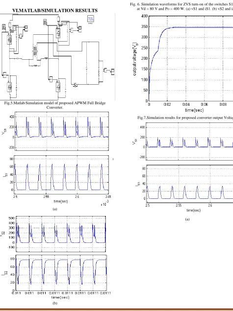
Fig.5.Matlab/Simulation model of proposed APWM Full Bridge Converter.
(a)
(b)
Fig. 6. Simulation waveforms for ZVS turn-on of the switches S1 and S2 at Vd = 80 V and Po = 400 W. (a) vS1 and iS1. (b) vS2 and iS2.
Fig.7.Simulation results for proposed converter output Voltage.
Available online:
https://edupediapublications.org/journals/index.php/IJR/
P a g e | 1440(b)
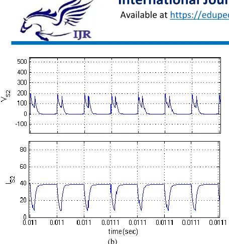
Fig. 8. Simulation waveforms for ZVS turn-on of the switches S1 and S2 at Vd = 40 V and Po = 400 W. (a) vS1 and iS1. (b) vS2 and iS2.
Fig.9.Simulation results for proposed converter output Voltage.
Fig.10.Matlab/Simulation model of PV system Based closed loop Control of proposed APWM Full Bridge Converter.
Fig.11.Simulation waveform of PV Voltage.
Fig.12.Output Voltage of Closed loop APWM full bridge Converter.
VII.CONCLUSION
Available online:
https://edupediapublications.org/journals/index.php/IJR/
P a g e | 1441power switches are clamped to the input voltage. Thus, the proposed converter has the structure to minimize power losses. These advantages make the proposed converter suitable for fluctuating input voltage on renewable energy conversion systems.Compared to traditional converter, they have enhanced system reliability to no shoot-through problems and lower switching loss with the help of using power closed loop control. The closed loop control, it theoretically eliminates the inherent current zero-crossing distortion of the single-unit asymmetrical type PWM full bridge converter. In addition, the closed loop control can greatly reduce the ripple current or cut down the size of passive components by increasing the equivalent switching frequency.
REFERENCES
[1] J. Zhang, H. Wu, X. Qin, and Y. Xing, “PWM plus secondary-side phase-shift controlled soft-switching full-bridge three-port converter for renewable power systems,” IEEE Trans. Ind. Electron., vol. 62, no. 11, pp. 7061–7072, Nov. 2015.
[2] K. C. Tseng, J. Z. Chen, J. T. Lin, C. C. Huang, and T. H. Yen, “High step-up interleaved forward-flyback boost converter with three winding coupled inductors,” IEEE Trans. Power Electron., vol. 30, no. 9, pp. 4696–4703, Sep. 2015.
[3] A. K. Rathore, A. K. S. Bhat, and R. Oruganti, “Analysis, design and experimental results of wide range ZVS active-clamped L-L type current fed dc/dc converter for fuel cells to utility interface,” IEEE Trans. Ind. Electron., vol. 59, no. 1, pp. 473–485, Jan. 2012.
[4] A. I. Bratcu, I. Munteanu, S. Bacha, D. Picault, and B. Raison, “Cascaded dc–dc converter photovoltaic systems: Power optimization issues,” IEEE Trans. Ind. Electron., vol. 58, no. 2, pp. 403–411, Feb. 2011.
[5] B. R. Lin and J. Y. Dong, “New zero-voltage switching DC–DC converter for renewable energy conversion systems,” IET Power Electron., vol.5, no. 4, pp. 393–400, Apr. 2012.
[6] Y. Shin, C. Kim, and S. Han, “A pulse frequency modulated full bridge DC/DC converter with series boost capacitor,” IEEE Trans. Ind. Electron., vol. 58, no. 11, pp. 5154–5162, Nov. 2011.
[7] I.-H. Cho, K. Cho, and G. Moon, “A new phase-shifted full-bridge converter with maximum duty operation for server power system,” IEEE Trans. Power Electron., vol. 26, no. 12, pp. 3491–3500, Dec. 2011. [8] Z. Chen, Q. Zhou, J. Xu, and X. Zhou, “Asymmetrical pulse-width modulated full-bridge secondary dual resonance DC–DC converter,” J. Power Electron., vol. 14, no. 6, pp. 1224–1232, Nov. 2014.
[9] Z. Ye, P. K. Jain, and P. C. Sen, “A full-bridge resonant inverter with modified phase-shift modulation for high-frequency AC power distribution systems,” IEEE Trans. Ind. Electron., vol. 4, no. 2, pp. 242– 247, Oct. 2007.
[10] Y. C. Hsieh and C. S. Huang, “Li-ion battery charger based on digitally controlled phase-shifted full-bridge converter,” IET Power Electron., vol. 5, no. 6, pp. 755–764, Oct. 2009.
[11] Y. Jang and M. M. Jovanovi´ c, “A new family of full-bridge ZVS converters,” IEEE Trans. Power Electron., vol. 19, no. 3, pp. 701–708, May 2004.
[12] S. H. Lee, C. Y. Park, J. M. Kwon, and B. H. Kwon, “Hybrid-type full-bridge DC-DC converter with high efficiency and wide input range,” IEEE Trans. Power Electron, vol. 30, no. 8, pp. 4156–4164, Aug. 2015.
[13] B. R. Lin, J. Y. Dong, and J. J. Chen, “Analysis and implementation of a ZVS/ZCS DC–DC switching converter with voltage step-up,” IEEE Trans. Ind. Electron., vol. 58, no. 7, pp. 2962–2971, Jul. 2011.
[14] H. Wu, P. Xu, and Y. Xing, “Series-input interleaved forward converter with a shared switching leg for wide input voltage range applications,” IEEE Trans. Ind. Electron., vol. 60, no. 11, pp. 5029– 5039, Nov. 2013.
AUTHOR’S DETAILS:
Sontyam, Anandapurm, Visakhapatnam, A.P, India. V.JAGADEESH Received his B.Tech Degree in EEE from VITS College of Engineering, Sontyam, Visakhapatnam, A.P in 2015. At Present pursuing M.Tech in VITAM College of Engineering, Sontyam, Visakhapatnam, A.P, India.