Study and Analysis of DC – DC Step down
Converter
Ubaidulla
1, Satish Kumar J
2, Malashree G.
3Assistant Professor, Department of Electrical & Electronics Engineering, HKBK College of Engineering, Bangalore, Karnataka, India 1,2,3
ABSTRACT: The main objective of this paper is to focus on the design and performance of a closed loop DC-DC buck converter system, which can be used to provide robust and high performance power point tracker acting as an intermediate between supply source and load for photovoltaic application. The proposed design includes PI controller for efficient steady state operation. The procedure in terms of selection of components has also been demonstrated. The system was simulated using Power Electronic Simulation (PSIM 9.0). This paper presents the simulation results of constant input voltage of 100V; the buck converter is able to produce 200 W with average 70 percent efficiency.
KEYWORDS: Step Down DC-DC Converter, PI controller, PSIM. I. INTRODUCTION
In recent decades, research on the use of photovoltaic as an alternative source of energy has become eminence in the field of electrical engineering [1]. A typical photovoltaic energy system compromises DV value at its output side. They are a promising technology and future energy demand in a sustainable and environmentally friendly way.
Photovoltaic is made up of cells (solar cell) which are wired together into a module. A number of these cells can be arranged together to produce a much higher voltage. The surface area of a cell and the intensity of the light hitting the panel determine the amount of current produced [2].
A number of modules can be arranged together either in parallel or in series. The amount of DC voltage depends on the arrangement of modules. For instance, four PV modules can reach out 300 Watts when connected in parallel and the value of its output voltage is high. Due to the load specification and the need to provide a lower voltage with high efficiency, a regulator or converter is required in most PV applications in order to step-down the output voltage that they generate. In addition, PV modules require an intermediate power point tracker as their characteristics are nonlinear [3].
The proposed topology in this work is DC-DC buck converter which has the voltage output lower than the input. In order to verify the design methodology, the system was simulated using Power Electronic Simulation (PSIM 9.0) software. The simulation results has shown that the efficiency has been achieved at an average of 70 percent with maximum output power produced of 200W.
II. BUCKCONVERTER
In a buck converter, the average output voltage VOis less than the input voltage Vi hence the name “Buck”, popularly
used as a DC regulator for PV application. The typical circuit diagram of a Buck Converter is as shown in the Fig. 1(a).There are four main components: switching power MOSFET S, freewheeling diode D, inductor L and output filter capacitor C. A switching control circuit monitors the output voltage, and maintains it at the desired level by switching „S‟ ON and OFF at a fixed rate, but with a varying duty cycle.
(a) (b)
(c)
Fig. 1DC-DC step down converter (a) Circuit diagram (b) Circuit Diagram for Charge Phase (c) Inductor Discharge Phase
The principle of operation of buck converter in CCM [5] can be explained in two phases: 1. Inductor charge phase and
2. Inductor discharge phase.
(i) Inductor charge phase: Figure (1b) gives equivalent circuit when switch S is ON. This phase is known as inductor charge phase. During this period, current begins flowing from the input source VS and inductor „L‟, and then into
capacitor „C‟ and the load (RL). The magnetic field in inductor L therefore builds up, storing energy in the inductor;
with the voltage drop across L opposing or „bucking‟ part of the input voltage. From the above circuit, we can write
𝑉𝐿= 𝑉𝑆− 𝑉0… … … . . 1
And
𝐿𝑑𝑖
𝑑𝑡= 𝑉𝑆− 𝑉0… … … . . (2)
Integrating equation (1) with respect to dt leads to
∆𝐼𝐿𝑐𝑎𝑟𝑔𝑒 =
𝑉𝑠− 𝑉0
𝐿 𝐷𝑇 … … … (3)
Where VS,Vo, D and∆𝐼𝐿𝑐𝑎𝑟𝑔𝑒are supplysource, output voltage, duty cycle and value of inductor current IL during
charge phase respectively.
From fig. 4,
𝑉𝐿= −𝑉𝐶= −𝑉0… … … 4
And
−𝑉0= 𝐿
𝑑𝐼𝐿
𝑑𝑡… … … (5)
Integrating equation (5) with respect to dt leadsto
∆𝐼𝐿𝑑𝑖𝑐 𝑎𝑟𝑔𝑒 =
−𝑉0
𝐿 (1 − 𝐷)𝑇 … … … (6)
Where VC is the value of voltage across the capacitor C and is the value of inductor current during discharge state.
(iii) Steady State Operation:Since change in average inductor current is zero [6], from equation (3) and equation (6) we get,
𝑽𝒔− 𝑽𝟎
𝑳 𝐷𝑇 −
−𝑉0
𝐿 1 − 𝐷 𝑇 = 0 … … … (7)
Therefore,
𝑉0= 𝐷𝑉𝑠… … … . . (8)
Where, „D‟ is the duty cycle which can be varied between 0 and 1. So, by varying the switching duty cycle the constant output voltage is obtained for any disturbance in the supply voltage.The current ratio between output and input will be the reciprocal of the voltage ratio; ignoring losses for a moment, andassuming our converter is perfectly efficient.
𝐼𝑜𝑢𝑡
𝐼𝑖𝑛 =
𝑉𝑖𝑛
𝑉𝑜𝑢𝑡… … … (9)
(iv) Condition for CCM: For the system to operate in continues conduction mode, Imin must be greater than zero
Where,
𝐼𝑚𝑎𝑥 = 𝑉0 1
𝑅+
1 − 𝐷
2𝐿𝑓 … … … . (10)
And
𝐼𝑚𝑖𝑛 = 𝑉0 1
𝑅−
1 − 𝐷
2𝐿𝑓 … … … . (11)
The minimum value of „L‟ required for operating the converter in CCM mode is given by,
𝐿𝑚𝑖𝑛 =
1 − 𝐷
2𝑓 𝑅 … … … (12)
The minimum value of „C‟ required for operating the converter in CCM mode is given by
𝐶 = 𝑉0
∆𝑉0
×1 − 𝐷
III.DESIGNOFPICONTROLLER
The Figure 2(a) shows block diagram proposed converter system. PI control is a traditional linear control method used in industrial applications. The linear PI controller controllers are usually designed for dc-dc converters using standard frequency response techniques and based on the small signal model of the converter. A Bode plot is used in the design to obtain the desired loop gain, crossover frequency and phase margin. The stability of the system is guaranteed by an adequate phase margin.
(a)
(b) (c)
Figure.2. Proposed system(a) block diagram (b) open loop buckconverter (c) Closed loop buck converter. However, linear PID and PI controllers can only be designed for one nominal operating point. The poles and a right -half plane zero, as well as the magnitude of the frequency response, are all dependent on the duty cycle. Therefore, it is difficult for the PID controller to respond well to changes in operating point. The PI controller is de signed for the buck converter for operation during a start-up transient and steady state respectively.
Figure 2(b) and 2(c) shows circuit diagram of open loop the closed loop of the dc-dc buck converter with PI controller. The load voltage of the proposed converter is given to the PI controller. Then the output of the PI controller changes the pulse width of the square wave which changes the firing angle of the MOSFET switch [6], so the output of the converter is controlled for different load disturbances.
IV.SIMULATIONRESULTS
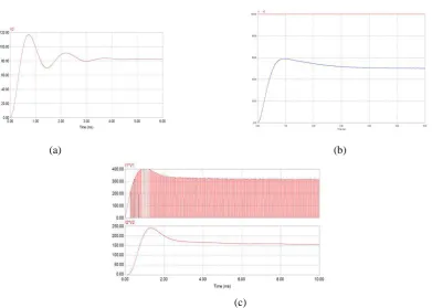
open loop system.The input power and output power of buck converter is studied and plotted as shown in the Fig. 3(c).The simulation of the Open Loop Buck Converter is as shown in the Fig. 3(a).
Input Output Rated Switching Load Voltage Voltage Power Frequency (RL)
100 V 50 V 200 W 25 kHz 16Ω Table 1: specifications of proposed converter
(a) (b)
(c)
Fig. 3(a) Output voltage waveform of open loop buck converter (b) Output voltage waveform of closed loop buck converter with VOUT = 50V (c) waveforms of input and output power of closed loop buck converter
V. COMPARATIVEEVALUATION
Many researchers explained open loop dc-dc buck converter as shown in the Fig. 2(b) with an average efficiency of 60 percent and with the constant input voltage. The proposed closed loop dc-dc buck converter as shown in the Fig. 2(c) and Fig. 3(b) reduces the steady state error with a regulated output voltage. The proposed design was able to produce 200 Watts with an average efficiency of 70 per cent as shown in the Fig. 3(c)
VI.CONCLUSIONANDFUTUREWORK
simulated with a feedback control. PI controller is used for feedback control. The output voltage is bucked and it is constant at steady state. It reaches the steady state value within several milliseconds.
In future we can change the load from resistive to Inductive load or motor load. This buck circuit can be implemented to control different special machines like switched reluctance motor, Brushless DC motor etc. We can also change the controller to intelligent controllers like neural network controller, fuzzy logic controller and neuro-Fuzzy logic controller.
REFERENCES
[1] P. C. M. Bernardo, Z. M. A. Peixoto, L.V. B. Machado Neto, “A high efficient micro-controlled buck converter with maximum power point tracking for photovoltaic systems”, International Conference on Renewable Energies andPower Quality Spain, April 2009.
[2] V. Meksarik, S. Masri, S. Taib, C. M.Hadzer, “Development of high efficiency boost converter for photovoltaic application”, National Power & Energy Conference (PECon) 2004 Proceedings, 2004
[3] M. Veerachary, “Fourth-order buck converter for maximum power point tracking applications,” IEEE Trans. On Aerospace and Electronic Systems, vol. 47, Issue No. 2, April 2011 pp 893-911
[4] S. Khader, “Design and simulation of a chopper circuits energized by photovoltaic modules”, 2011 IEEE GCC Conference and Exhibition (GCC) United Arab Emirates, February 2011.
[5] SyafrudinMasril, NorizahMohamad, Muhammad Hafeez Mohamed Hariri “Design and development of DC-DC buck converter”, IEEE Conference on Power Engineering and Renewable Energy 2012, 3-5 July 2012, Bali, Indonesia
[6] R.Laksh mi, X. Felix Joseph, Dr.S.Pushakumar, D.Arun Dominic, “Design simulation and analysis of a soft switching scheme for dc-dc boost converter with a closed loop controller” proceedings of ICETECT 2011