Reduction of Power and Delay using Single
Event Transient Suppressor for Sequential
Elements
B.Rajagnanapazham
1, P.Alagesan
2Assistant Professor, Dept. of Electronics and Communication Engineering, Sasurie College of Engineering, Tiruppur, Tamilnadu, India 1&2
ABSTRACT: The simulation results shows that the circuit with SET suppressor consumes less power, reduction of
glitches and delay is also reduced when compared with the conventional circuit. This shows that SET suppressor efficiently A chip is often affected by environmental radiations due to its reduced size and low operating voltages. This causes a bit flipping in internal nodes of sequential elements which is known as single event upset (SEU). This also causes glitches in the combinational part of the digital circuit which is known as Single Event Transient (SET). This SET may cause an error while reading the flip flop. Due to glitch formation and error by SET overall power dissipation and delay is increased. To reduce the power consumption and delay we propose a SET suppressor. The SET suppressor includes two OR gates, a NAND gate, an AND gate and an inverter. In synchronous sequential circuits SET suppressor circuit can be used for feeding clock signals which reduces glitches thereby reducing the power consumption. To measure the performance of the proposed SET suppressor , an ordinary D flip flop circuit and another D flip flop circuit with SET suppressor is taken and implemented in MICROWIND reduces the power ,delay and glitches.
KEYWORDS: Single Event Upset, Single Event Transient
.
I. INTRODUCTION
With the decrease of feature size and reduction of operating voltage of advanced chips, sensitivity to radiation increases drastically. A single radiation event may cause bit flipping in an internal node of the sequential elements, which is called single event upset (SEU). A single radiation event may also cause a glitch in the combinational part of a digital circuit, which is called single event transient (SET). A SET may propagate through the combinational circuit to sequential elements and result in an error. This leads to increased susceptibility of SRAM, latches and flip- flops to SETs/SEUs.SET/SEU happens and may cause the stored value of a latch or a flip-flop to be incorrectly inverted.
For space applications, neutrons, protons and heavy cosmic ions which are trapped in geomagnetic belts produce intense showers of such radiation. When such ions strike diffusion regions in VLSI designs, they can deposit a charge, resulting in a voltage spike on the affected circuit node. If the magnitude of this spike is sufficiently large, an erroneous value may be computed by the circuit. This is particularly problematic for memories, since the stored state can flip as a result of such a radiation strike. Combinational logic may also be affected by such strikes, if the resulting glitch occurs at the time the circuit outputs are being sampled. This bit reversals are also called as Single Event Transients (SETs).
With the relentless shrinking of the minimum feature size of VLSI Integrated Circuits (ICs), there is a corresponding reduction in the dimensions of diffusion nodes. This results in a reduced diffusion capacitance, and hence, if charge is dumped on the diffusion node as a consequence of a radiation strike, a large voltage spike may be generated. With operating voltages getting smaller, this problem is further aggravated.
minimize this glitch occurrence and to minimize the power and delay of the Flip Flops. Here we design a Single Event Transient Suppressor for Flip Flops which reduces glitches which in turn reduces the power dissipation of the CMOS circuit.
A SET suppressor for flip-flops, which can mitigate Single Event Transient (SET) pulses having a width less than T, where T is the longest anticipated duration of SETs. The advantage of this technique is that it only introduces little flip-flop delay when no SET occurs near the capturing clock edge, which is a majority of time.
The rest of the paper is organized as follows. Section II describes the typical rising-edge triggered master-slave flip-flop. Section III presents the proposed Single Event Transient Suppressor for Flip Flops. Section IV compares the results with existing method and the Section V includes the concluding remarks.
II RISING EDGE TRIGGERED MASTER SLAVE FLIP-FLOP
A typical rising-edge triggered master-slave flip-flop is shown in the Fig.1.The flip-flop includes a data input D and a clock input CLK. From the CLK input, internal complementary clock signals CLN and CL are created. When CLK is logic low, the internal clock signals CLN and CL enable the master D latch so that the logic state on the data input D is written into the master latch. This allows the master latch to store the data input value when the clock signal transitions from low to high. As CLK goes high, CL and CLN disable the master latch and the data input value is locked. Nearly simultaneously, when CLK transitions from low to high, the slave D latch transitions from a disabled state to an enabled state.
This allows the signal captured at the rising edge of the clock to pass through the slave latch. When CLK returns to low, the output Q of the slave latch is locked, and the value seen at the last rising edge of the clock is held, while the master latch begins to accept the new values in preparation for the next rising clock edge. The SEUs in the feedback loops of the flip-flop can be mitigated with schemes .
However, if a SET in the upstream combinational circuits propagates to the data input D near the capturing clock edge, erroneous data may be captured by the master latch, flow through the slave latch, and be provided at the data output Q, even if the flip-flop is SEU-hardened.
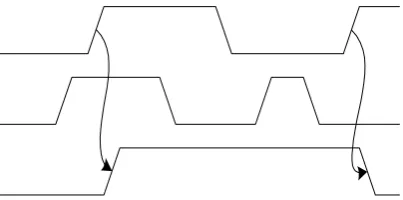
Fig. 1. Rising-Edge Triggered Master Slave Flip-Flop The Fig. 2 explains about the operation of the Rising Edge
Triggered Flip Flop is shown in above figure . It shows that whenever the CLK rises, D is copied to Q . At all other times, Q holds its value.
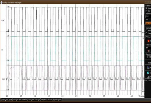
The Fig. 3 shows the layout design of the rising Edge Triggered Master Slave Flip Flop drawn in MICROWIND 3.1.The output waveform for the Rising Edge Triggered Master Slave Flip Flop is also obtained as shown in the Fig. 4.The output waveform shows the presence of glitches and the power consumption by the Flip Flop.
Fig. 3. Layout of Rising-Edge Triggered Master Slave Flip-Flop
Fig. 4. Waveform of Rising-Edge Triggered Master Slave Flip-Flop
III SINGLE EVENT TRANSIENT SUPPRESSOR FOR FLIP-FLOPS
A. Proposed Single Event Transient Suppressor for Flip- Flops
Single event upset (SEU)-hardened flip-flops cannot mitigate single event transients (SET) that come from the upstream combinational circuits and propagate to the data inputs of flip-flops near the capturing clock edge. This part presents a SET suppressor that can mitigate such SETs. By adjusting the clock edge timing so that the flip-flop captures data when the data returns to a correct state, the SET suppressor protects a flip-flop against SETs.
provide complementary clock signals to the flip-flop (in Fig. 1). The clock circuit increases the flip-flop hold time after a data transition near the capturing clock edge of the flip-flop. An internal data state of the flip- flop is used to adjust the timing of the clock edges. . If the data transition occurs near the clock sampling edge, the clock timing is adjusted so that the data input continues to be sampled for a period beyond the normal hold time. Thus, the hold time is increased when the data transition occurs near the clock sampling edge, so that the flip-flop captures data when the data returns to a correct state.
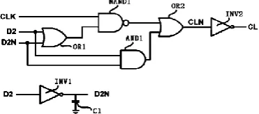
Fig. 5Single Event Transient Suppressor for Flip Flops
As seen from Fig. 5, the clock circuit includes two OR gates OR1 and OR2, a NAND gate NAND1, an AND gate AND1 and an inverter INV2. The clock circuit receives three inputs, the input clock signal (CLK), an internal data state of the flip-flop (D2) and an inverted internal data state input (D2N),and outputs complementary clock signals (CL, CLN) to the flip flop.signal CLK, the output clock signal CL (applied to the flip-flop), the data input D and output Q (of the flip- flop). The dashed line 602 represents the normal hold time of the flip-flop, while the dashed line 604 represents the hold time after adjustment by a time period (the adjustment is achieved by the delay in the rising edge of CL) in the presence of a SET near the capturing clock edge.
In scenario #1, the data input D is not impacted by a SET pulse. D is low when the clock (CLK/CL) transitions from low to high. As the flip- flop is rising-edge triggered, the data output Q transitions from high to low as expected.
In scenario #2, the data input D is impacted by a SET pulse having a relatively long duration. D is expected to be low at the rising edge of the clock signal CLK, but the SET pulse changes D to high before the rising edge of CLK. Because the SET pulse lasts longer that the longest adjustable hold time indicated by line 604, the data output Q remains high. So the flip-flop stores incorrect data.
In scenario #3, the data input D is impacted by a SET pulse having a relatively short duration. D is expected to be low at the rising edge of the clock signal CLK, but the SET pulse changes D to high near the rising edge of CLK. However, because the SET pulse
duration is relatively short, D returns to the correct
state before the longest adjustable hold time indicated by line 604. Accordingly the rising edge of the clock signal CL is delayed to the time before line 604. Thus, the flip-flop latches the correct data despite the SET.
Fig. 6. Timing Diagram of SET Suppressor
The tuning capacitor adds a delay (that is the longest anticipated SET duration) for pulse migration from D2 to D2N. The capacitance of the capacitor C1 may control the duration of the delay but may not affect the setup time of the flip-flop. This is because the inverter INV1 and the capacitor C1 are not in either the feedback loop of the master latch or the data path between the master and slave latches of the flip-flop.
As seen from Fig. 6 , there is no delay in the data transition on the output Q of the flip-flop under normal conditions. When a SET occurs near the clock (CLK) edge, the data transition on Q will be later than the normal time at which Q would change due to the increased hold time that may allow the end of the SET pulse having a relatively short duration. The allowable increase in hold time is adjusted by the tuning capacitor C1 in Fig. 5 (because C1 controls longest adjustable delay in the rising edge of CL).
The allowable increase in hold time should be adjusted with care to avoid a failure of a setup time on a latch whose input is derived from the Q output of the latch that has a SET on its input D. If the clock cycle is long enough to provide sufficient setup time and hold time (when a SET occurs near the capturing clock edge), the SET-induced flip-flop will maintain synchronization with other normal flip-flops and will not violate timing requirements for the next (non-SET) clock cycle.
The flip-flops using the proposed SET suppressors are typically useful in mixed asynchronous and synchronous circuits. When a SET occurs near the capturing clock edge, the flip-flop output is delayed and hence may cause delay in the downstream asynchronous circuits. The delayed outputs of the asynchronous circuits may cause the delay in the downstream synchronous circuits. However, when no SET occurs near the capturing clock edge, there will be no such delay.
IV RESULTS AND DISCUSSION
Fig. 7. Layout of SET Suppressor
The resulting waveforms are obtained and the power dissipation value is noted for both the circuits. The simulation results shows that the circuit with SET suppressor consumes less power, reduction of glitches and delay is also reduced when compared with the conventional circuit.
This shows that SET suppressor efficiently reduces the power, delay and glitches.
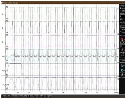
Fig. 8. Output Waveform of SET Suppressor
Copyright to IJIRSET www.ijirset.com 342
(a)
(b)
(c)
Fig. 9. Comparision of (a)Power consumption (b) Delay and (c) Power Delay Product of Edge
Triggered Master Slave Flip Flop and D Flip Flop with SET Suppressor
Similarly the delay analysis of Edge Triggered Master Slave Flip Flop and D Flip Flop with SET suppressor that the delay of proposed D flip-flop with SET suppressor decreases by 7%. Finally, the Power Delay Product analysis of Edge Triggered Master Slave Flip Flop and D Flip Flop with SET suppressor shows that the Power Delay Product of proposed D flip-flop with SET suppressor decreases by 7.2%. This shows the performance of D Flip Flop with SET Suppressor is better than the performance of Edge Triggered Master Slave Flip Flop.
V. CONCLUSION
the flip-flop input to filter out SETs, but this increases flip-flop delay regardless of whether a SET is occurring. The proposed SET suppressor can mitigate SETs by adjusting the clock edge timing. The SET suppressor only increases very little flip-flop delay when no SEU occurs near the capturing clock edge, which is a great majority of time .Moreover the power consumption is reduced in our proposed method when compared with conventional method. Simulation results demonstrate that the proposed scheme has better performance than SET filters. Future work can be carried out in implementing CMOS circuits by using a voltage level convertor and the proposed SET suppressor for further reduction in power dissipation .
REFERENCES
[1] D. R. Blum and J. G. Delgado-Frias, “Delay and energy analysis of SEU and SET-tolerant pipeline latches and flip- flops,” IEEE Trans. Nucl. Sci., vol. 56, no. 3, pp.1618–1628, Jun. 2009.
[2] T. Calin, M. Nicolaidis, and R. Velazco, “Upset hardened memory design for submicron CMOS technology,” IEEE Trans. Nucl. Sci., vol.43, pp. 2874 - 2878, Dec. 1996.
[3] M. Fazeli, A. Patooghy, S. G. Miremadi, and A. Ejlali, “Feedback redundancy: A power efficient SEU-olerant latch design for deep submicron technologies,” in Proc. 37th Annu. IEEE/IFIP Int. Conf. Dependable Systemsand Networks, Jun. 25–28, 2007, pp. 276–285.
[4] J. Singh, J. Mathew, M. Hosseinabady, and D.K.Pradhan, “Single event upset detection and correction,” in Proc. 10th Int. Conf. Information Technology, Dec. 17–20,2007, pp. 13–18.