ABSTRACT
BAEK, SEUNGHUN. High-Frequency AC-link Transformers for Medium-Voltage DC/DC Converters and Solid State Transformer Applications. (Under the direction of Subhashish Bhattacharya.)
Traditional electricity systems rely heavily on easily accessible fossil fuels, such as coal and natural gas. However, the price of these finite sources has been increasing rapidly, and the com-bustion of these fossil fuels have caused considerable damage to the environment. The utilization of clean local energy resources, such as solar, wind, ocean energy, etc. is no longer a viable op-tion in preparing for the shortage of these finite natural resources or avoiding environmental pollution.
In order to efficiently link local renewable energy to the power grid, there is a critical demand for modernized and functional distribution systems. The core element of the future smart distribution system is the power electronics-based distribution transformer made using power semiconductor devices, also known as the Solid-State Transformer (SST).
State-of-the-art power electronics applications using enhanced DC technology for high-voltage, high-frequency applications have taken center stage recently for levels in the range of tens of kW to MW. Power electronic applications using developing 15kV SiC devices to di-rectly support distribution line voltage is a challenging work and derives many related topics. Designing and implementing medium-voltage, AC-link transformers in an isolated DC/DC stage of an SST at an operating frequency of 20kHz is one of the challenging tasks in the realization this technology.
This thesis contains comprehensive design considerations for medium-voltage and medium frequency(MV-MF) AC-link transformers for SST applications under operations of different types of high-power dual-active bridge DC/DC converters. The main goal of this thesis is to understand the operation and system characteristics of the DC/DC conversion stage of SST, and design the most suitable and optimized magnetic components for these specific applications. Specifically, the inductor-integrated coaxial winding transformer (ICWT) and three winding low-profile transformer are designed for these specific applications and studied in this thesis for the first time. Detailed studies into steady-state operations for different types of MV-MF DAB DC/DC converters and transformers, including inductor integration, switching response with parasitic effects, loss characterization, and experimental verification, are carried out. Computer-aided design and finite element analysis (FEA) are intensively used for detailed study.
High-Frequency AC-link Transformers for Medium-Voltage DC/DC Converters and Solid State Transformer Applications
by Seunghun Baek
A dissertation submitted to the Graduate Faculty of North Carolina State University
in partial fulfillment of the requirements for the Degree of
Doctor of Philosophy
Electrical and Computer Engineering
Raleigh, North Carolina 2014
APPROVED BY:
Alex Huang Jayant Baliga
ACKNOWLEDGEMENTS
First of all, I would like to show my sincere appreciation for the opportunities and support by Prof. subhashish bhattacharya. I couldn’t have completed all the hard work without him, and my colleagues at the FREEDM System Center at North Carolina State University.
Furthermore, I want to express my gratitude to Prof. Dr. Huang, Dr. Baliga and Dr. Stancil for serving as committee members for my Ph.D. exam and for their effort to evaluate my thesis. Many thanks go to all my friends who shared hard times and their thoughts in United States in the past year.
Finally, to my family, father, mother, elder brother and his lovely wife and kids, Hyenjin and Hyengjun, and Stephanie who have supported me with love and patience.
TABLE OF CONTENTS
LIST OF TABLES . . . vi
LIST OF FIGURES . . . .viii
CHAPTER 1 Introduction . . . 1
1.1 Current state of the solid state transformer applications . . . 1
1.2 Medium-voltage and medium-frequency AC-link transformers for SST applications 4 1.2.1 Topologies of SST applications using bidirectional isolated DAB DC/DC conversion . . . 4
1.2.2 Chapter overview . . . 11
1.3 Motivations and contributions . . . 14
1.3.1 Importance of the magnetics components in AC-link section of the iso-lated high-power DC/DC converter . . . 14
1.3.2 Contributions . . . 15
CHAPTER 2 EXISTING BIDIRECTIONAL AND ISOLATED DAB DC/DC CONVERTERS . . . 16
2.1 DAB DC/DC converter operations and scope of the study . . . 16
2.1.1 Investigated topologies of DAB DC/DC converter . . . 16
2.1.2 Understanding power flow and soft switching of DAB operation using fundamental frequency component . . . 17
2.1.3 Modulation schemes of DAB DC/DC converter . . . 18
2.2 Single-phase dual active bridge (DAB) DC/DC converter . . . 20
2.2.1 Steady state lossless operation - Single phase DAB . . . 20
2.2.2 Soft switching schemes - single phase DAB DC/DC converter . . . 23
2.2.3 Influence of a finite magnetizing inductance with an asymmetric impedance matrix . . . 25
2.3 Three-phase dual-active bridge converter topology - Yy connection . . . 32
2.3.1 Steady state lossless operation Three phase Yy connection . . . 32
2.3.2 Soft switching scheme - Three phase Yy connection . . . 34
2.4 Summary . . . 35
CHAPTER 3 MEDIUM-FREQUENCY AND MEDIUM-VOLTAGE COAX-IAL WINDING TRANSFORMER . . . 37
3.1 Summary of transformer design equations and parameters . . . 38
3.2 Modeling coaxial winding transformer (CWT) with parasitic effects . . . 43
3.2.1 Configuration of CWT and prototype . . . 43
3.2.2 Geometric simplification and meshing considerations for finite element analysis . . . 45
3.2.3 Inductance modeling and calculation for CWT . . . 48
3.2.4 Parasitic capacitances modeling of CWT . . . 53
3.3 Skin and proximity effects on concentrically arranged windings . . . 66
3.3.1 Skin and proximity effect . . . 66
3.3.2 EM field distribution on an infinite tubular conductor - review of literatures 67 3.3.3 Proximity effect on conductors in concentric geometry . . . 70
3.3.4 Computer aided FEM results in 3D for CWT prototype . . . 72
3.4 Insulation strategy for MV-MF CWT prototype for SST application . . . 77
3.4.1 Electric filed distribution in simple configurations of insulation . . . 77
3.4.2 Insulation strategy and case study for MV-MF CWT . . . 78
3.5 MV-MF CWT prototype and experimental test results . . . 85
3.5.1 Loss and insulation test results . . . 85
3.6 Summary . . . 87
CHAPTER 4 PROPOSED INDUCTOR-INTEGRATED COAXIAL WIND-ING TRANSFORMER FOR DAB DC/DC CONVERTER . . . 88
4.1 Modeling concept: Inductance integration . . . 91
4.1.1 Lumped-element equivalent inductance model of ICWT . . . 91
4.2 Selection of materials and dimensions of cores . . . 98
4.2.1 Selection of core material . . . 98
4.2.2 Dimension optimization of the cores . . . 100
4.3 Proposed loss formula for ICWT for phase-modular single phase DAB DC/DC converters . . . 103
4.3.1 Cores properties . . . 103
4.3.2 Loss characteristics with DAB DC/DC conversion operation . . . 106
4.4 High frequency effect on a multi-tubular conductor with harmonics components . 109 4.5 Insulation strategies for MV-MF ICWT prototype . . . 113
CHAPTER 5 ICWT PROTOTYPE IMPLEMENTATION AND EXPERI-MENT RESULTS . . . .116
5.1 Loss Characteristics of the ICWT prototype . . . 117
5.1.1 Eddy and proximity effects in real geometry and consideration on the auxiliary parts . . . 117
5.1.2 Inner and outer core losses . . . 125
5.1.3 Operation region of ICWT prototype with SiC-based 6kVDC/400VDC DAB DC/DC converter . . . 126
5.2 ICWT with SiC-based 6kVDC/400VDC DAB DC/DC stage of SST . . . 132
5.2.1 The switching response of the ICWT with 15kV SiC MOSFET under DAB operation . . . 132
5.3 Loss and temperature measurement of ICWT under operation at 10kVA . . . 136
5.4 Summary . . . 139
CHAPTER 6 PROPOSED THREE-PORT AND THREE-PHASE DAB CON-VERTER IN Yyd CONFIGURATION . . . .140
6.1 Winding types and considerations on three-phase system . . . 140
6.2 Three-phase DAB converter topology - Yd connection . . . 142
6.2.2 Soft switching scheme three phase Yd connection . . . 145
6.3 Proposed three-port three-phase bidirectional and isolated dc/dc converter in Yyd connection . . . 147
6.3.1 Power flow analysis using network calculations and impedance model . . . 147
6.3.2 Steady state lossless operation - Three phase in Yyd connection . . . 149
6.3.3 Soft switching scheme Three phase Yyd connection . . . 151
6.4 Proposed inductor integrated three-winding planar transformer for the proposed topology . . . 155
6.4.1 Modeling concept : inductance matrix of a three winding planar trans-former and geometrical analysis . . . 155
6.4.2 Winding arrangement and inductance calculation . . . 155
6.4.3 FEM transient simulation results and comparison with analytical solution 157 6.5 Comparison and implementation of laboratory prototype . . . 162
6.6 Prototype implementation and experiment results . . . 167
CHAPTER 7 Conclusions . . . .170
7.1 Summary and conclusion . . . 170
REFERENCES . . . .175
Appendices . . . .180
Appendix A . . . 181
LIST OF TABLES
Table 1.1 Specifications of SST Gen.1 transformer and AC-link transformer . . . 8
Table 1.2 Specifications of the AC-link transformer prototypes . . . 8
Table 1.3 Specifications of the Lab. prototype A . . . 9
Table 1.4 Specifications of the Lab. prototype B . . . 12
Table 3.1 Field distribution . . . 44
Table 3.2 Specifications of the AC-link transformer prototype [mm] . . . 50
Table 3.3 Leakage permeance calculated by finite element method in 2 dimension . . 52
Table 3.4 Permeance measurement from the prototype (The length of the body is 0.6m) . . . 52
Table 3.5 Measurement conditions . . . 59
Table 3.6 Calculation results . . . 60
Table 3.7 Current density on coppers in series connection at 100kHz . . . 67
Table 3.8 Current density on coppers in parallel connection at 100kHz . . . 68
Table 3.9 Electric field intensity in simple geometry . . . 78
Table 3.10 Rated withstand voltages . . . 79
Table 3.11 Electric stress . . . 80
Table 3.12 Specifications of the windings and insulation materials . . . 81
Table 3.13 Switching condition of a half bridge configuration . . . 82
Table 3.14 Insulation medium : Insulation oils and air . . . 82
Table 3.15 Insulation medium : Epoxy resins . . . 83
Table 3.16 Dielectric breakdown test results without active cooling method . . . 85
Table 3.17 Pulse switching test results without active cooling method . . . 85
Table 3.18 AC resistances of LV and HV winding at 20kHz . . . 86
Table 4.1 Operating condition . . . 94
Table 4.2 Specification of the outer cores and inner cores . . . 94
Table 4.3 Equations . . . 101
Table 4.4 Coefficients of specific loss of MPP cores on datasheets . . . 102
Table 4.5 Loss and size comparison (Sinusoidal excitation, line current =3.33 [Arms]) 102 Table 4.6 Coefficients of specific loss of 0.0007” Nanocrystalline . . . 103
Table 4.7 Specific loss of MPP cores at 20kHz, 0.1T (ID: 14.7mm, OD:26.9mm, HT: 11.2mm)) . . . 105
Table 4.8 Loss coefficients of inner and outer cores . . . 108
Table 4.9 Fourier series quantities of trapezoidal waveform with phase shift 30◦ at 20kHz, 1Arms . . . 109
Table 4.10 AC resistance [uΩ/m] with thickness and frequency . . . 111
Table 4.11 AC resistance [uΩ/m] with thickness of trapezoidal current waveform with DAB DC/DC operation phase shift 30◦ at 20kHz . . . 112
Table 4.12 Rated withstand voltages IEC60076-3 . . . 113
Table 4.13 Electric stress at power frequency . . . 114
Table 4.15 Specifications of the windings and insulation materials . . . 115
Table 5.1 Specifications of LV winding [mm] . . . 118
Table 5.2 Specifications of inner and outer cores . . . 133
Table 5.3 Parasitic elements . . . 134
Table 5.4 Specifications of the single phase DAB DC/DC converter for loss measure-ment . . . 137
Table 5.5 ICWT with 2.7mH inductance integration (efficiencyη) . . . 138
Table 5.6 ICWT with 4.0mH inductance integration (efficiencyη) . . . 138
Table 6.1 Dimensions of the proposed planar transformer . . . 158
Table 6.2 Specifications . . . 159
Table 6.3 Terminal leakage inductances . . . 159
LIST OF FIGURES
Figure 1.1 Electric power transmission in United States . . . 2
Figure 1.2 Current status of the MV-MF transformer with rated frequency and voltage 3 Figure 1.3 Current status of the MV-MF transformer with rated frequency and power 3 Figure 1.4 Conceptual diagram of SST applications . . . 5
Figure 1.5 Isolated high power resonant/ non-resonant type DC/DC converters . . . 5
Figure 1.6 The first generation SST with IGBT-based cascaded DC/DC stage . . . 8
Figure 1.7 15kV SiC Mosfet based single-stage 6kVDC/400VDC DAB converter . . . 9
Figure 1.8 The transformer less Intelligent Power Substation (TIPS) . . . 12
Figure 1.9 1200V IGBT based three-port three-phase DAB DC/DC converter in Yyd configuration . . . 13
Figure 2.1 One line diagram and phasor diagram of DAB operation . . . 18
Figure 2.2 Circuit mode of operation under zero voltage switching . . . 19
Figure 2.3 One line diagram and vector notation with parasitic effects . . . 19
Figure 2.4 Single-phase DAB converter in half bridge configuration . . . 20
Figure 2.5 One-line diagram with square wave excitation . . . 21
Figure 2.6 Waveforms of Single phase DAB DC/DC converter operation with phase-shift modulation and Power transfer with phase-phase-shift modulation of a single-phase DAB DC/DC converter . . . 22
Figure 2.7 Real and average apparent power withθpsandk(Red line : Soft switching boundaries) . . . 24
Figure 2.8 (a) P i(Delta) network, (b)T(W ye) network . . . 26
Figure 2.9 Simplified diagram of single phase DAB converter with T network model . 27 Figure 2.10 Lossless circuit model with finite magnetizing inductance . . . 27
Figure 2.11 Po Lm/Pmax with ’m’ and ’χ’ . . . 28
Figure 2.12 ZVS region withk,χand m. . . 29
Figure 2.13 Current waveforms with finite magnetizing inductance . . . 31
Figure 2.14 Three-phase DAB DC/DC converter topology in Yy connection . . . 32
Figure 2.15 Waveforms of a three-phase DAB DC/DC converter in Yy connection . . 33
Figure 2.16 Line current waveforms of single phase DAB converters . . . 34
Figure 2.17 Real and average apparent power withθpsandk(Black line : Soft switch-ing boundary) . . . 35
Figure 3.1 Relationship between variables in Eq3.3 . . . 40
Figure 3.2 Transformer design flow chart . . . 42
Figure 3.3 Solenoid winding transformer . . . 43
Figure 3.4 Coaxial winding transformer . . . 45
Figure 3.5 Assembly . . . 46
Figure 3.6 Prototype of MV-MF coaxial winding transformer . . . 47
Figure 3.7 Simplification of curved surface, (a)18 segments (b) 12 segments (c) 6 segments (d) Square shape based on the cross sectional area . . . 47
Figure 3.9 Skin depth based mesh generation and field distribution (a)3 layers on round shape (80 elements) , (b) 2 layers on round shape(42 elements), (c) 1 layers on round shape(24 elements), (d) 1 layers on square shape based
on the cross sectional area . . . 49
Figure 3.10 Computation error with skin depth based mesh generation (a)Inductance , (b) Resistance . . . 49
Figure 3.11 Views onr−z plane (left) andr−φplane (right) . . . 50
Figure 3.12 Dimensions and winding arrangement . . . 51
Figure 3.13 Leakage magnetic field distribution in CWT . . . 53
Figure 3.14 6 capacitance equivalent circuit model . . . 54
Figure 3.15 Simplified capacitance equivalent circuit model . . . 58
Figure 3.16 Impedance modulus and argument [◦] with frequency [Hz] of the CWT prototype . . . 62
Figure 3.17 Equivalent circuit model of CWT (∼1/4λ) . . . 63
Figure 3.18 E-field distribution in connection of each measurement . . . 63
Figure 3.19 A circuit representation from HV side by transmission line theory in the range of 1/4λ∼30MHz . . . 64
Figure 3.20 Zin in the range of 3MHz ∼30MHz . . . 64
Figure 3.21 Switching response with step voltage excitation on the LV side . . . 65
Figure 3.22 Switching response with step voltage excitation on the HV side . . . 65
Figure 3.23 Electric field intensity vs. normalized thickness . . . 69
Figure 3.24 Current density and magnetic field intensity vs. normalized thickness . . . 70
Figure 3.25 Current density in a tubular conductor,√2[A] current excitation at 20kHz 71 Figure 3.26 Current density in a outer tubular conductor,√2[A] current excitation in outer tubular conductor and −√2[A] in inner tubular conductor at 20kHz 71 Figure 3.27 Normalized ac resistance vs. thickness at 20kHz (ri = 60mm) . . . 72
Figure 3.28 Field distribution . . . 73
Figure 3.29 Multi-tubular winding . . . 74
Figure 3.30 Current density distribution in 2D (IHV peak = √ 2[A],ILV peak= 30· √ 2[A]) 74 Figure 3.31 Effective resistance on LV and HV windings . . . 75
Figure 3.32 Field distribution . . . 76
Figure 3.33 Concentric winding arrangement . . . 80
Figure 3.34 E-field distribution with insulation medium (Mineral oil) . . . 83
Figure 3.35 E-field distribution with insulation medium (air) . . . 83
Figure 3.36 E-field distribution with insulation medium (Epoxy resin) . . . 84
Figure 3.37 Test set-up . . . 86
Figure 3.38 Temp. distribution after 60 minites operation of the pulse switching test . 87 Figure 4.1 Assembly of ICWT . . . 90
Figure 4.2 Prototypes of ICWT . . . 90
Figure 4.3 Cross sectional views . . . 91
Figure 4.4 Equivalent circuit model . . . 92
Figure 4.5 One quarter of a simplified model for 3D FEM transient solution . . . 95
Figure 4.7 Transient waveforms of an ICWT in a single-phase DAB DC/DC
conver-sion at θps=π/4 . . . 97
Figure 4.8 Inductor integration in coaxial winding transformer . . . 99
Figure 4.9 Volume, Weight, Length and loss comparison with respect to the ratioro/ri101 Figure 4.10 Outer cores . . . 104
Figure 4.11 Specific loss measurement of MPP cores . . . 105
Figure 4.12 Specific losses vs magnetic flux density at 20kHz . . . 106
Figure 4.13 DAB DC/DC converter atk= 1 with phase-shift modulation . . . 109
Figure 4.14 trapezoidal current waveform . . . 110
Figure 4.15 Copper tubes . . . 111
Figure 4.16 AC resistance of the multiple of copper tubes . . . 112
Figure 4.17 Winding arrangement . . . 113
Figure 4.18 E-field distribution in 2D (Excitation : V1=60kV,V2=V3=0, insulation medium : epoxy resin) . . . 114
Figure 5.1 ICWT prototype with aluminum case and heatsinks- Machine shop built assembly . . . 117
Figure 5.2 Tubular copper and connecting copper for LV winding of ICWT . . . 118
Figure 5.3 Effective resistance on LV windings . . . 118
Figure 5.4 Current density on LV winding of the ICWT prototype in 3D . . . 119
Figure 5.5 Current density distribution on the HV winding (Excitation : inner wind-ing -1Arms, outer windwind-ing 1Arms) . . . 122
Figure 5.6 H-field distribution at 10kHz . . . 123
Figure 5.7 Effective resistance on HV windings . . . 124
Figure 5.8 Eddy current in an aluminum case (Excitation : HV winding 3.33Arms, LV winding:51.0A with magnetizing current at 20kHz) . . . 124
Figure 5.9 Configurations with ratio roc o/roc i,m . . . 125
Figure 5.10 Efficiency of the ICWT laboratory prototype withm and load condition 126 Figure 5.11 Loss and real power transfer vs. load . . . 127
Figure 5.12 Efficiency vs. load (η= Pin−Ploss Pin ) . . . 128
Figure 5.13 Loss measurements from ICWT Prototype withC055927A2 and compar-ison with analytical solution (turns ratio 1:1) . . . 128
Figure 5.14 Heat pathes from hot-spot to the case and heatsink . . . 129
Figure 5.15 Waveforms of open-circuit tests (turns ratio 4:1) . . . 130
Figure 5.16 B-H curve at 20kHz . . . 130
Figure 5.17 Nominal operation region of the laboratory prototype, SiC based single-phase DAB 6kVDC/400VDC converter and ICWT with C055925A2 . . . 131
Figure 5.18 The SiC-based 6kVDC/400VDC DAB DC/DC stage of SST with an in-ductor (3.8mH) integrated coaxial winding transformer . . . 133
Figure 5.19 Impedance plot (turns ratio 15:1) . . . 134
Figure 5.20 Equivalent lumped circuit model of high frequency switching response . . 134
Figure 5.23 The configuration of the test set-up, 1200V IGBT-based DAB DC/DC
converter for load-test . . . 136
Figure 5.24 1200V IGBT-based DAB DC/DC converter test set-up using NI Crio and LabviewFAPGA . . . 137
Figure 5.25 Thermal images of ICWT with C055925A2 (mur = 200) at 10.9kVA, 10.1kW and total transformer loss of 360W . . . 138
Figure 6.1 One line diagram of a three-port three-phase bidirectional isolated DAB DC/DC converter in Yyd connection . . . 141
Figure 6.2 Three phase DAB in Yd connection . . . 142
Figure 6.3 Waveforms in Yd connection . . . 143
Figure 6.4 Line current waveforms (k= 1/√3) . . . 146
Figure 6.5 Real and average apparent power withθpsandk(Red line : Soft swathing boundary) . . . 146
Figure 6.6 Proposed three-port three-phase bidirectional and isolated dc/dc con-verter in Yyd connection.) . . . 148
Figure 6.7 SimplifiedW ye-type (left) andDelta-type (right) primary-referred equiv-alent circuit of three port system) . . . 149
Figure 6.8 One line diagram of DAB operation and vector notation for voltage and current in phasor form ) . . . 150
Figure 6.9 One line diagrm Proposed three-port three-phase bidirectional and iso-lated dc/dc converter in Yyd connection) . . . 151
Figure 6.10 Line current waveforms in winding 1 . . . 152
Figure 6.11 Current waveforms referred to the primary winding . . . 153
Figure 6.12 Real and average apparent power withθpsandk(Red line : Soft swathing boundary) . . . 154
Figure 6.13 Terminal leakage inductances measurements . . . 156
Figure 6.14 Leakage magnetic field intensity distribution in planar window area . . . . 157
Figure 6.15 H-field distribution - Top view . . . 158
Figure 6.16 Inductance integrated planar MV-MF transformer . . . 159
Figure 6.17 Winding arrangement . . . 159
Figure 6.18 Transient behavior during proposed three-winding planar transformer with three-phase and three port DAB DC/DC converter 3D FEM tran-sient solution . . . 160
Figure 6.19 Current waveforms on HV side of single-phase DAB (blue, topology 2) and phase current waveforms on HV side of three-phase DAB in Yyd connec-tion (red, topology 3) - the same DC-link voltages and line inductance are applied . . . 161
Figure 6.20 VA rating on HV side . . . 164
Figure 6.21 VA rating on LV side . . . 165
Figure 6.22 Ratio between real and average apparent power (T/P) . . . 166
Figure 6.23 Prototype of MV-HF series inductance integrated planar transformer . . . 167
Figure 6.24 Laboratory prototype . . . 168
Chapter 1
Introduction
1.1
Current state of the solid state transformer applications
Solid-state-transformer (SST) is a power conversion system made of high power semiconductor components with control circuitry. The concept of the solid-state transformer (SST) dates back to the 1980’s, but the major obstacles slowing down the development and commercialization of SST applications at distribution-line levels are the lack of high-frequency, high-power capac-ity power semiconductor devices, and suitable circuit components such as transformers. Like the commercialization of the IGBTs, which led to a considerable increase in capacity of the power-electronics applications in the 90’s, the new materials such as a Silicon Carbide (SiC) devices, high frequency magnetic materials, and a variety of soft-switching techniques under zero-voltage or zero current conditions, allows high-power conversion at higher frequency at a medium voltage level. The operation condition of the solid-state-transformer is, literally, at the limit of commercially available power devices and passive circuit components. With that being said, the reliability of the distribution line applications cannot be compromised.
appli-Generating station Generator
Transmission line custoner 138kV, 230kV
Transmission substation Distribution substation
Main transmission
138kV, 230kV, 345kV, 500kV,765kV
Sub-transmission 115/121kV, 60/69kV Generation Subtransmission Customer Customer 120V/240V Distribution
11/12kV, 13.8kV, 35kV
Generator step-up transformer
Step-down Large power transformer
Distribution transformer
(1~20 customers)
Step-down Power transformer
Figure 1.1: Electric power transmission in United States
cations come from its reductions in size and weight. Locomotive-traction applications can take full advantage of SST applications with respect to size and provide even more attention to this technology in Europe, where the locomotive industry is prevalent.
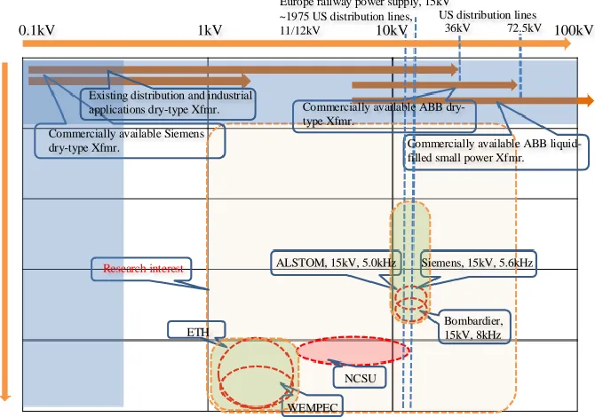
Even though the results and specifications of the prototypes developed in academia and industry are highly limited, the current status of the development of SST applications is plotted on the basis of published papers and reports, shown in Fig 1.2 and Fig 1.3. Most of the medium voltage-high frequency(MV-HF), or medium voltage-medium frequency(MV-MF), transformers are developed for resonant or DAB DC/DC modular converters. The clear tendency of power and voltage ratings of MV-MF transformers is seen differently in academia and industry. The applications developed in industry usually have higher power and voltage ratings, which could be related to the capability of the testing facilities. However, the switching frequency of prototypes developed in industry rarely goes up to 5 kHz even though present power devices are capable of that frequency. This is likely a result of the considerations of size, efficiency and marketability. The insulation level required at medium voltage by the international standards considerably offsets the size and cost reduction at high switching frequency. The power rating of the complete system ranges from several kW up to several MW, but it is made of several converter modules and a single module rarely exceeds 500kVA as seen in Fig 1.3. The voltage rating is typically between 10kV to 15kV which is the practical voltage level in distribution lines and railroad lines in Europe.
0.1kV 1kV 10kV 100kV
Existing distribution and industrial
applications dry-type Xfmr. Commercially available ABB dry-type Xfmr.
Commercially available ABB liquid-filled small power Xfmr.
Siemens, 15kV, 5.6kHz Bombardier, 15kV, 8kHz ALSTOM, 15kV, 5.0kHz
ETH
NCSU WEMPEC Commercially available Siemens
dry-type Xfmr.
Research interest
~1975 US distribution lines, 11/12kV
Europe railway power supply, 15kV
US distribution lines 36kV 72.5kV
Figure 1.2: Current status of the MV-MF transformer with rated frequency and voltage
1kVA 10kVA 100kVA 1MVA 10MVA 100MVA
60Hz 400Hz 2kHz 10kH 50kHz Research interest
Existing distribution and industrial
applications dry-type Xfmr. Commercially available ABB dry-type Xfmr.
Commercially available ABB liquid-filled small power Xfmr.
Commercially available Siemens dry-type Xfmr. Siemens, 450kV, 5.6kHz Bombardier, 350kW, 8kHz ALSTOM, 180kW, 5.0kHz ETH NCSU WEMPEC ABB,
75kW, 400Hz Siemens, 270kW, 350Hz
15MVA 63MVA
1.2
Medium-voltage and medium-frequency AC-link
transform-ers for SST applications
The term, medium voltage, is typically used in the range of 1kV to 35kV (ANSI/IEEE 1585-2002, IEEE Std 1623-2004), however this term is a rather conventional working definition and varies with international standards and references (teh Dept. of Energy defines medium voltage up to 138kV in transmission voltage class). It is reasonable to consider that a distribution line is in the range of medium-voltage (MV), and many next-generation switching converters are targeting for medium-voltage and medium-frequency, or high-frequency, applications. The solid-state transformer is the key elements in the Future Renewable Electric Energy Delivery and Management (FREEDM) Systems. It is acting as an energy router to enable active management between distribution line and distributed energy resources with the features like instantaneous voltage regulation, voltage-sag compensation, power-factor correction and DC output. Speaking of the size of the SST applications, the isolated DC/DC stage is one of the key elements that has isolation transformers. The MV-MF transformers for high-power DC/DC converter appli-cations at tens of kHz switching frequency, especially DAB and resonant DC/DC converters, are recently receiving a lot of attention. The MV-MF transformer is a critical element in the DC/DC conversion stage of SST applications because SST applications require galvanic iso-lation at medium-voltage distribution line and the high conversion ratio between distribution line and end users cannot be efficiently achieved without consideration of the turns ratio of the transformer. Additionally, the required series inductance to store energy and transfer power in the DC/DC conversion stage can be replaced by a leakage inductance of the transformer, or integrated into the transformer. This can provide a considerable improvement with respect to power density and system reliability. Optimization and series-inductance integration are one of the recent active research topics for high-power DC/DC converter applications.
1.2.1 Topologies of SST applications using bidirectional isolated DAB DC/DC conversion
SST applications developed in the FREEDM Systems Center has three conceptual stages, AC/DC, DC/DC and DC/AC as shown in Fig 1.4. A rectifier on the front-end converts the conventional AC line voltage to DC in the medium voltage range. The medium-voltage DC is then converted to low- voltage DC at the voltage level of end users through a high frequency AC-link. The LVDC can be used for DC applications or further conversion to 50/60Hz AC for existing consumer applications.
Rectifier DG, Consumer Inverter
MV DC LV DC
P Isolated DC/DC stage
Controller MV-MF transfomer
Conventional LV AC LV DC Conventional
MV AC
Figure 1.4: Conceptual diagram of SST applications
AC-Link
Step up/down MV-MF transformer
L, R, C (resonant/ non-resoant type)
+
Isolated DC/DC stage
Figure 1.5: Isolated high power resonant/ non-resonant type DC/DC converters
6.5kV IGBT based cascaded DAB DC/DC converter
The first generation of the solid-state transformer (SST) applications developed in FREEDM Systems Center is implemented with existing 6.5kV Silicon IGBT power devices in a cascaded configuration in Fig. 1.6 [13]∼[20]. The prototype is designed and implemented with an emphasis on SST concept verication. The input is single-phase 7.2 kVAC from the distribution line and single-phase DAB DC/DC converters are cascaded in the DC-link stage due to limitations of the blocking voltage of the silicon-based power devices in Fig 1.6. The voltage stress on the power devices and AC-link transformer is reduced to 3.8kVAC at the switching frequency 3 kHz. The three AC-link transformers are built in the conventional manner, with an amorphous alloy. The required series inductance for the DC/DC conversion stage is achieved through the leakage inductance of the AC-link transformer. The leakage inductance of the transformer is adjusted by changing the winding arrangement and the number of turns. The specifications of the prototypes are shown in the Table 1.1. Iterative numerical study with finite-element method simulation was conducted for optimization. The total power density of up to 1.0kV A/cm3of the transformers at switching frequency 3kHz was achieved and measured by experiment, installed of an IP00 according to IEC standard.
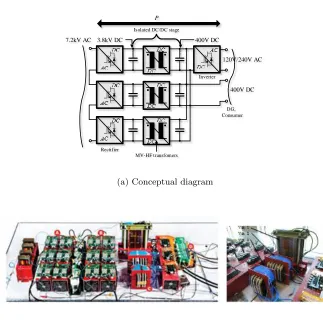
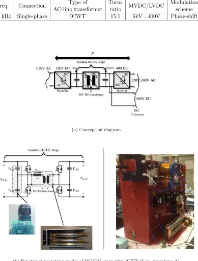
15kV SiC Mosfet based single-stage DAB DC/DC converter
A 15kV SiC MOSFET based SST is implemented with an emphasis on efciency improvement and size reduction. The power electronics applications at distribution voltage level has been built by series devices and multilevel configurations at today’s semiconductor voltage level (6.5kV for silicon device and 10kV for SiC MOSFET). Collaboration and development of the 15kV SiC MOSFET by CREE Inc. and the FREEDM systems center allows a single stage of a DAB DC/DC converter with the minimum number of circuits at operating frequencies up to 20kHz. The single-phase DAB DC/DC converter is composed of a single HF transformer and two active bridges, which are the half-bridge circuits shown in Fig 1.7 (b). The DC/DC conversion stage is comprised of the high-voltage terminal 12kV and low-voltage terminal at 400V. The switching frequency is determined by considering device switching losses of the 15kV SiC MOSFET under development. The laboratory prototype A was built at half scale of the real application, at 6kVDC/400V, to be within a practically applicable range at the FREEDM Systems Center of NSF’s ERC headquarter in Fig 1.7.
Rectifier
DG, Consumer
3.8kV DC 400V DC
P
Isolated DC/DC stage 7.2kV AC
120V/240V AC
400V DC
MV-HF transfomers
Inverter
(a) Conceptual diagram
(b) Pictures with AC-link transformers (2009)
Figure 1.6: The first generation SST with IGBT-based cascaded DC/DC stage
Table 1.1: Specifications of SST Gen.1 transformer and AC-link transformer Freq. Turns VA MVDC : LVDC Required series Modulation
ratio inductance scheme
3 kHz 9.5:1 20kVA 3.8kV : 400V ∼30mH Phase-shift
Table 1.2: Specifications of the AC-link transformer prototypes Core
kVA Lm[mH] Ll[mH]
Total
Power density
Material loss
Ver. 1
Metglas
SA2605SA1 6.7kVA
235 36 227 W 0.4kV A/dm3
Ver. 2 469 30 194 W 0.8kV A/dm3
Table 1.3: Specifications of the Lab. prototype A
Freq. Connection Type of Turns MVDC/LVDC Modulation AC-link transformer ratio scheme 20 kHz Single-phase ICWT 15:1 6kV : 400V Phase-shift
Rectifier
DG, Consumer
12kV DC 400 DC
Isolated DC/DC stage
7.2kV AC
120V/240V AC
400V DC
MV-HF transfomer P
Inverter
(a) Conceptual diagram
n : 1
Isolated DC/DC stage
MV-MF transfomer
(b) Functional prototype model of DC/DC stage with ICWT (Lab. prototype A)
Proposed 12kV SIC IGBT based three-phase and three-port DAB DC/DC con-verter
The transformer less Intelligent Power Substation (TIPS) is a 15kV IGBT and 1200 V SiC-MOSFET based SST applications used to connect between the three-phase distribution grid and distributed resources[14], [15]. The TIPS system also follows the three-stage configuration of AC/DC, DC/DC and DC/AC in Fig 1.4 with the three-phase concept to reduce the VA rating of power devices and filter components. The 22 kVDC from the three-phase rectifier is stepped-down to 400VDC through three-phase DAB DC/DC converters with 12kV/10A SIC IGBT co-pack modules. The input stage handles 100 kVA while interfacing with the 13.8 kV utility grid in Fig 1.8. TIPS has a phase-modular three-port DC/DC converters in the iso-lated DC/DC stage inW ye−W ye and Delta (Yyd) connection. Two voltage-source inverters, VSIs, in parallel are used on the LV side to divide the high current on the LV side and reduce losses. The two VSIs are connected in aW ye andDelta connection respectively to avoid third harmonics issues in three-phase AC systems.
1.2.2 Chapter overview
Chapter 1: The current status of the existing SST applications and the scope of the study are discussed. The topologies, system specifications and design considerations of the laboratory prototypes being built in FREEDM Systems Center are introduced.
Chapter 2 : The existing DAB high- power and high-frequency DC/DC converters, single-phase and three-single-phase in Yy connection, are reviewed. The operation principles of both DAB converters are explained based on lossless ideal switching models. Analytical modeling approach under piece-wise linear operation is reviewed for both topologies. The power flow, RMS ratings and zero-voltage switching region with control variables are analytically calculated and shown. Chapter 3 : The MV-MF coaxial-winding transformers (CWT) is analytically studied with parasitic effects, core and copper losses, and medium-voltage insulation perspective. The simple lumped-element equivalent circuit model is introduced to understand the high-frequency response including common-mode voltage. The switching and insulation test have been done at 20kHz and 6kVAC with the MV-MF CWT prototype. Computer aided design and finite element analysis are intensively used for detailed study of effects on high frequency electromagnetic fields.
Chapter 4: The proposed new concept of inductor-integrated coaxial winding transformer (ICWT) is analytically studied and verified. The design methodology including selection of the core material, size optimization and operational boundaries is also discussed. Loss equation with the system parameter and control variable in single-phase DAB DC/DC converter is derived and verified by measurement results. The auxiliary losses from complex geometry, such as Litz wire, case and connectors, are achieved through computer-aided finite-element analysis tools.
Chapter 5 : The ICWT prototype is built and the feasibility of the new concept is veri-fied by experiment. 1200V IGBT-based DC/DC converter is built to collect data for detailed loss model in a wide operation range. Overall efficiency of ICWT is mapped based on the proposed loss equation to find maximum efficiency, and is compared to the loss measurement. Medium-voltage switching and operation tests are implemented by 15kV SiC-based single-phase 6kVDC/400VDC conversion stage of the SST application at power transfer of 7kVA.
Rectifier
DG, Consumer
22kV DC 400 DC
Isolated DC/DC stage
3Ф 13.8kV AC
120V/240V AC 400V DC
Proposed 3port-3phase isolated DAB DC/DC
converter P
(a) Conceptual diagram
Front End Converter
Dual Active Bridge
Low Voltage Side Inverter
13.8 kV, 3-phase, 60Hz grid
15kV SiC IGBT based 3L-NPC Modular Structure
15kV/20A SiC IGBT/JBS Diode Co-pack module
480 V, 3-phase, 60Hz grid 22 kV DC Bus
800 V DC Bus
(b) Topology
Figure 1.8: The transformer less Intelligent Power Substation (TIPS)
Table 1.4: Specifications of the Lab. prototype B
Freq. Connection Type of Turns DC/DC Modulation
AC-Link
DC power
Personal Computer NI CompactRIO
LabviewFPGA
(a) Configuration of proposed three-port three-phase DAB DC/DC converter with three-winding planar transformers
(b) Functional prototype model of DC/DC stage with NI Compact Rio and LabviewFPGA (Lab. prototype B)
1.3
Motivations and contributions
1.3.1 Importance of the magnetics components in AC-link section of the isolated high-power DC/DC converter
Size and efficiency are the essential desirable characteristics and results of the design and imple-mentation of power-conversion system. The magnetics design is therefore of great importance in the design of power electronics applications. It is well known that the size, weight and cost of magnetic components are a strong function of operating frequency. Without considering thermal limits and efficiency requirements, increasing operating frequency by high-frequency switching provides inversely-proportional size reduction of magnetic cores, however, leads to nearly proportional increase in switching losses on the power device. The high-power DC/DC converters, typically resonant and DAB-type DC/DC converters, in AC-link section is fully op-erating in AC operation without DC components; this is especially true for high-power DC/DC converters. The AC component of the current, which is the source of the magnetic flux variation and loss in magnetic material, has an even stronger relationship with the loss and size. Hence, the magnetic components and resonant and DAB type high power DC/DC converters are even more connected through switching frequency and system parameters. The transformer design has to take many design constraints into account, such as material properties, efficiency, ther-mal limits, and parasitic effects while considering material properties. The optimization process necessarily requires a good understanding of circuit operation.
Isolation protection is necessary for a grid voltage level to protect against electric shock and comply with strictly observed international standards. The advent of solid sate transformer ap-plications does not mean that electromagnetic induction-based transformers will be eliminated by solid-state circuit elements. The galvanic isolation by electromagnetic induction of trans-formers will not be replaced by electronic circuit components at the medium voltage level as of yet. Besides that, the high conversion ratio between grid and end users is still hard achieve with only switching operation at an acceptable efficiency. Therefore, a high frequency isola-tion transformer is still a critical part in solid-sate transformer applicaisola-tions, and increasing the operating frequency of isolation transformers in medium-voltage level is an emerging research area.
are difficult, high-risk and requires costly procedures. Therefore, predicting and planning the performance of the transformer under a wide range of operation conditions with accuracy is another significant advantage for minimizing the cost and risks. The design of the magnetics components is always one of the main issues and objectives of high-power and high-frequency DC/DC converters. The key feature in the operation of resonant and DAB type DC/DC con-verters is fully predicting and utilizing the transformer without external inductors to transfer power and achieve zero-voltage switching. Therefore, the main goal of this thesis is under-standing the operation and system characteristics of the MV-MF DC/DC conversion stage and designing suitable and optimized magnetic components for these specific applications.
1.3.2 Contributions
1. Propose a unique design of an inductor-integrated coaxial winding transformer(ICWT) and analytical design methodology including operating mechanism and size optimization. 2. Implement a prototype of the ICWT for 6kVDC/400DC stage of a SST application and
verify the new concepts.
3. Conduct computer aided design and finite element analysis(FEA) for detailed study of effects on high frequency electromagnetic fields.
4. Propose and analyze the steady-state operation of the new phase-modular three-port three-phase DAB DC/DC converter.
5. Propose unique design of inductor-integrated three winding planar transformer suitable for three-port three-phase DAB DC/DC converter.
6. Build and test hardware prototypes of scaled-down prototypes of 1200V IGBT-based three-port three-phase DAB DC/DC converter using NI CompactRio and LabviewFPGA .
Chapter 2
EXISTING BIDIRECTIONAL
AND ISOLATED DAB DC/DC
CONVERTERS
2.1
DAB DC/DC converter operations and scope of the study
2.1.1 Investigated topologies of DAB DC/DC converter
The dual-active-bridge DC/DC converter is one of the most prominent non-resonant type con-verters featuring bidirectional power flow and galvanic isolation for high frequency and high power DC/DC conversion. It consists of one series inductance, used as a filter, at the high fre-quency AC-link section. The filter element does not necessarily exist as separate element, and can be replaced by parasitic elements of the system such as leakage inductance of the trans-former. Both converters at the front and end stages convert DC to high frequency AC for the high frequency isolation transformer at the AC-link section.
Typically, full-bridge or half-bridge circuits are used for single-phase DAB DC/DC oper-ation, while three-leg bridges are used for three phase DAB DC/DC operation. The isolation by AC-link transformers and soft-switching techniques are essential aspects to making DAB DC/DC conversion suitable for MV-MF/HF applications. The symmetric circuit structure with actively controlled power devices provides the bidirectional power transfer, and ensures the VA rating and stress on each component is evenly shared. The buck-boost operation with switching converters provides another degree of freedom in control.
In this thesis, the following different topologies are investigated, including the newly pro-posed three-port three-phase DAB converter in Yyd connection for SST applications :
2. Three-phase DAB DC/DC converter in Yy connection 3. Three-phase DAB DC/DC in Yd connection
4. Proposed three-port three-phase DAB DC/DC in Yyd connection (Lab. prototype B) For comparison, the VA rating of the AC-link transformer on both the LV and HV sides, and the soft-switching region during lossless steady-state operation are studied for each topology. These characteristics are the essence of DAB DC/DC operation and critical design parameters for the power conversion system.
2.1.2 Understanding power flow and soft switching of DAB operation using fundamental frequency component
Power flow of the two port inductance model in harmonic form
It is useful to understand the system’s behavior with fundamental frequency components, which has a major impact on system performance. Conceptually, the operation of DAB converter can be seen as an inductor excited by two voltage sources,v16 0 andv26 θ12, with a phase difference
of θ12, such as the synchronous machine shown in Fig 2.1. Provided that all circuit quantities
are sinusoidal at a single fundamental frequency, the steady-state current flow is represented in phasor notation in Eq 2.1.
iLs =
v26 0−v16 θ12
jωLs
(2.1) Hence, the real power is represented in harmonic form by :
P = v1v2sinθ12
ωLs
(2.2) Two important concepts in dual-active bridge operation are easily perceived by the pha-sor diagram. The bidirectional power flow between any two ports is equally possible, and the direction is only determined by the phase shift.
This calculation results from using the fundamental frequency components by phasor nota-tion in Eq 2.2 and actual models during piece-wise linear operanota-tion in Eq. 2.7, and shows good agreement between the two. Note that v16 0 and v26 θ12 in Eq 2.2 are the rms value, which is
2√2/π times of the peak value of the square waveform.
Soft switching region of the two port inductance model in harmonic form
(a) (b)
Figure 2.1: One line diagram and phasor diagram of DAB operation
Fig 2.2. Zero-voltage switching (ZVS) is achieved when a turn-on signal is applied to the switch while the anti-parallel diode is on. This switching process of a leading bridge of DAB converter can be represented in a phasor diagram as the line current iLs6 δ lags v16 θ12 in Fig 2.1. We learn that the line current always lagsv16 θ12and leadsv26 0 when the magnitude of the voltage
vectors are the same . This is an important design parameter for determining the soft switching region of DAB operation for high frequency switching. In the case where the step-up down iso-lation transformer is used, full controllability over the entire switching region is achieved when the turns ratio of the transformer is the same as the conversion ratio of the DC/DC stage.
The influence of the parasitic elements in the circuitry can simply be estimated with the phasor notation. The dominant parasitics of DAB converters, such as parasitic capacitances of devices and transformer windings and magnetizing inductance of isolation transformers, influence the soft switching region as shown in Fig 2.3. Soft switching is lost at lightly loaded conditions because parasitic capacitances always exist in real circuitry. There are existing studies about utilizing the magnetizing inductance of the isolation transformer to compensate the leading current through the parasitic capacitances with lagging current through the magnetizing inductance. By decreasing the magnetizing inductance, the load appears to lag more and the soft switching region is extended [20].
2.1.3 Modulation schemes of DAB DC/DC converter
1
2
Figure 2.2: Circuit mode of operation under zero voltage switching
(a) (b)
Figure 2.3: One line diagram and vector notation with parasitic effects
2.2
Single-phase dual active bridge (DAB) DC/DC converter
The single phase DAB converter consists of two voltage sourced full bridge or half bridge circuits. Both active bridge circuits are connected through an AC-link which consists of a high frequency isolation transformer and series inductance.
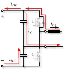
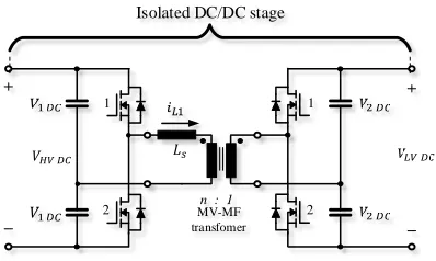
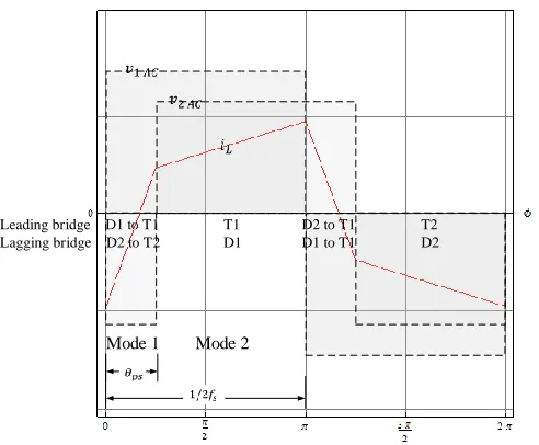
The circuit model of the laboratory prototype A is shown in Fig 2.4, which was comprised of half-bridge circuits. Regardless of the topology of the bridges, the DAB converter model can be simplified with a one line diagram with one series inductance Ls as a power transfer element, and two time varying voltage sources v1AC and v2AC in Fig 2.5. The direction of the power flow is determined by the phase shift between two bridgesθps, and the amount of power flow is controlled by bothθps and the series inductance Ls.
The analysis for the steady state operation of the DAB DC/DC converters is based on the following assumptions:
1. DC capacitors are infinitely large and the supplied DC voltage is constant.
2. The AC-link stage is comprised of an ideal transformer and series inductance without parasitic effects.
3. The power devices operate as a lossless ideal on-off switch, without parasitic effects.
n : 1
Isolated DC/DC stage
MV-MF transfomer
1 1
2 2
Figure 2.4: Single-phase DAB converter in half bridge configuration
2.2.1 Steady state lossless operation - Single phase DAB
Figure 2.5: One-line diagram with square wave excitation
of θ = ωt, where ω is the switching frequency. The following calculations are based on the positive power flow from the HV side to the LV side in the range of 0≤θps < π.
Two modes of operation are identified for a half switching cycle, and for the rest a half cycle is mirrored. Each side of the half bridge configuration has two different voltage levels +V1DC and −V1DC, and +V2DC and −V2DC respectively. The line inductance current repeats every half cycle with reversed sign during steady-state operation, and represented by piecewise linear functions. The general equation of the line inductance currentiL1 is represented by:
iL1[θ] =
v1AC−n·v2AC
Lsω
·(θ−θi) +iL1[θi] (2.3) where iL1[θi] is the initial current of each mode.
The line current in each mode is represented with the voltage state of both bridges in Eq 2.4
Mode 1: 0≤θ < θps,(v1AC =V1DC, v2AC =−kV1DC)
iL1 1[θ] =
v1DC(1 +k)
ωLs
·θ+iL1 1[0] (2.4)
Mode 2: θps≤θ < π,(v1AC =V1DC, v2AC =kV1DC)
iL1 2[θ] =
v1DC(1−k)
ωLs
·(θ−θps) +iL1 2[θps] (2.5)
With system conversion ratio G= V2DC
V1DC and buck-boost conversion ratiok=n·G
From the symmetry condition, iL1 1[0] = −iL12[π] and iL11[θps] = iL1 2[θps], the initial inductance current values are obtained in Eq 2.6.
iL1 1[0] =−
V1DC ωLs
(π(1−k)
2 +dθps), iL1 1[θps] =iL1 2[θps] =−
V1DC ωLs
(π(1−k)
2.24 0.58
Mode 1 Mode 2
Leading bridge D1 to T1 T1 D2 to T1 T2 Lagging bridge D2 to T2 D1 D1 to T1 D2
Figure 2.6: Waveforms of Single phase DAB DC/DC converter operation with phase-shift modulation and Power transfer with phase-shift modulation of a single-phase DAB DC/DC converter
The amount of power transfer in the DAB DC/DC converter is represented by the function of θps and Ls between two bridges is:
Po = 1
Ts
Z Ts
0
v1ac[t]·iL1[t]dt=
kV12DC(π−θps)θps
ωLsπ
(2.7)
θps is controlled by circuit control during operation and Ls is a fixed design parameter which has to be planned when it is designed according to the requirements of the system. The power flow is bidirectional and the maximum power transfer occurs atθps = π2 under the given condition in Eq 2.8
dPo
dθps = kV
2
1DC(π−2θps)
ωLsπ
= 0 (2.8)
Thus, the maximum power transfer of the single-phase DAB DC/DC converter for any given
kis :
Po max=
kπV12DC
4ωLsπ
(2.9) On the basis of the aforementioned assumption, the voltage gain ktheoretically varies with
applicable operating range, in practice, is approximately 0.5 to 1.5.
The root mean square (RMS) values of the voltage and current is of importance when choosing the rating of components and design of the isolation transformer. The rating of the transformer is determined by apparent power on the basis of the rms values, which determines the dimensions of the magnetic core and windings, rather than real power transfer. Assuming the magnetizing current does not exist, the rms value of the line current iL1rms with PSM is given by:
iL1rms= 1
ni2rms =
1
T
Z Ts
0
i2L1[t]dt=
V1DC
q
((d−1)2π3+ 12kπθ2
ps−8kθps3 )
ωLs2
√
3π (2.10)
The square wave with a duty ratio of 0.5,v1rms and v2rms respectively are represented by:
v1rms=V1DC, v2rms =n·V2DC (2.11) Hence, the power rating of the transformer is:
TV A=
v1rms·i1rms+v2rms·i2rms
2 =
(1 +d)v1rms·i1rms
2 (2.12)
2.2.2 Soft switching schemes - single phase DAB DC/DC converter
Zero-voltage switching is one of the essential properties of DAB DC/DC converter operation in making this topology suitable for high-power and high frequency operation. The power devices are turned on while the anti-parallel diode is conducting, so the voltage seen from the power device is nearly zero during switch-on transition. The calculation results are in per unit with base numbers:
Vb =V1DC, Ib=
Vb
ωL, Pb=VbIb. (2.13)
To meet this operating condition for each bridge, For the leading bridge :iL1[0]≤0,
iL1[0]≤0, k≤
1 1−2θps/π
(2.14)
For the lagging bridge :iL1[θps]≥0,
iL1[θps]≥0, k≥
π−θps
Fig 2.7 (a) shows theoretically achievable real power transfer and soft switching boundaries for the leading and lagging bridges with the phase shiftθps andkunder steady-state operation. The average value of the VA ratings on both sides, which is typically considered VA rating of the transformer, is shown in Fig 2.7 (b). The design parameters can be chosen based on the required power rating of the application, and controllability under soft-switching.
The soft-switching region is defined between the boundaries on both bridges. It should be noted that full control through the entire operation range can be achieved whenkis unity. How-ever, reduction of the soft switching region due to parasitic capacitances has to be considered in practice. As the variable k is increased, meaning the transformer’s turns ratio is decreased for the same system conversion ratio, the maximum power transfer is also increased with the same inductance value. The same power transfer can be achieved with a lower inductance value, size, and cost with respect to the magnetics components, however, the soft-switching region is also reduced under low load conditions. Losing soft-switching at high-power and high-frequency applications can not only considerably increase the switching losses of the power devices, but also damage the power devices and lead to system failure. Therefore,kis typically limited near unity value unless different modulation schemes are considered for low load condition. This is only applicable with a full-bridge circuit configuration, or if the power converter is designed for very constant load conditions.
0 Π 4 Π 2 0 0.5 10 Π 4 Π 2 0 0.5 1 0 Π 4 Π 2 0 0.5 10 Π 4 Π 2 0 0.5 1
2.2.3 Influence of a finite magnetizing inductance with an asymmetric impedance matrix
Utilization of the finite magnetizing inductance for DAB operation
In more practical approach, the magnetizing current of the isolation transformer is taken into account. The magnetizing inductance of a transformer is usually considered as an infinite num-ber for simplicity but, as matter a of fact, there is always a finite numnum-ber for the magnetizing inductance in the magnetic components.
Even though the influence of the magnetizing inductance on DAB DC/DC converters has been studied in literature, only a few put weight on the influence of an asymmetrical configu-ration of the AC-link section. It is customary to assume that the impedance matrix of isolation transformers is diagonally symmetric, and the leakage inductance on each winding is fairly similar. Conventional transformers are generally built in a symmetric manner in symmetric structure, which is a mostly solenoidal structure, hence the leakage magnetic flux of each wind-ing shares space under a balanced condition. However, the coaxial windwind-ing transformer (CWT) or the ICWT introduced in this thesis has a considerably different structure and asymmet-ric impedance matrix in concentasymmet-ric geometry. Therefore, it is worth recognizing the effect of the asymmetric structure and impedance matrix in case where the magnetizing inductance is considerable when compared to the series inductance, Ls.
There is no such difference between transformers and inductors, physically, besides the design purpose and functionality. The magnetizing inductance of transformers has not been a design parameter because it does not play a role as a circuit element. However, it can also be adjusted using the gap between cores, such as inductors or material change. As stated in the previous chapter, it is possible to utilize the effect of the magnetizing inductance to extend the soft switching region of a DAB DC/DC converter by purposefully increasing the lagging current.
A port network is used for circuit analysis with pairs of terminals through which current enters and leaves as a port. The four terminal or two port system is represented by an 2×2 impedance or admittance matrix when the system is a lossless and linear electrical circuit. Hence, two winding transformers can be seen as a 2-port system of the 2×2 impedance matrix with pure inductance elements, without considering the parasitic effects of the capacitances and resistances in Eq 2.16.
"
Z11 Z12
theoreti-cally identical in different circuit configuration. In this analysis, aW yeequivalent circuit model with lumped elements is used, which considerably reduce the complexity of the calculation with respect to circuit analysis.
Considering the inductances of the transformer are referred to as the one side for simplicity, the lumped elements of the T network can be seen as leakage inductance on winding 1 ’L1’,
leakage inductance on winding 2 ’L2’, and the magnetizing inductance ’Lm’. Hence, the lossless circuit representation is depicted without the parasitic effects of winding capacitances in Fig 2.10
Lm=L12≈Z12 (2.17)
L1 =L11−L12≈Z11−Z12 (2.18)
L2 =L22−L12≈Z11−Z12 (2.19)
L1 and L2 does not have to be the leakage inductance of the transformer itself, and they
can be external or integrated inductors. The series inductance Ls for power transfer, which is the sum ofL1 and L2, is the major factor of power transfer for DAB operation. We are going
to give a weight factor to the system symmetry of ’χ’ and an impact of magnetizing inductance ’m’.
L1 =χ·Ls, (0< χ <1) (2.20)
L2=Ls−χ·L1 (2.21)
Lm= (Lp+Ls)·m (2.22)
Hence, the general equations of iL1 and iL2 referring to theV1 DC side is represented by:
+
-+
-+
-+
+
-+
-Figure 2.9: Simplified diagram of single phase DAB converter withT network model
AC-Link
HV side LV side
n : 1
Figure 2.10: Lossless circuit model with finite magnetizing inductance
iL1[θ] = (
V1DC
ω(L1+L2 kLm)
− n·V2DC
ω(L2+L1kLm)
)· Lm
Lm+L1
·(θ−θi) +iL1[θi] (2.23)
iL2[θ] =−(
V1DC
ω(L2+L1 kLm)
− n·V2DC
ω(L1+L2 kLm)
)· Lm
Lm+L2
·(θ−θi) +iL2[θi] (2.24)
whereiL1[θi] andiL2[θi] are the initial currents of the each mode. If the magnetizing current
Lm is not large enough, it may considerably influence the line currents iAC1 and iAC2. The
amount of power flow in DAB converter operation with phase-shift modulation is revised with finite magnetizing inductance and system symmetry in Eq 2.25.
Po Lm =
k mV2
1DCφ(π−φ)
πωLs(m+χ−χ2)
0 0.5 1 0.6
0.7 0.8 0.9 1
m=5
m=3
m=1
Figure 2.11: Po Lm/Pmax with ’m’ and ’χ’
Po Lm =
m
m+χ−χ2 ·Po (2.26)
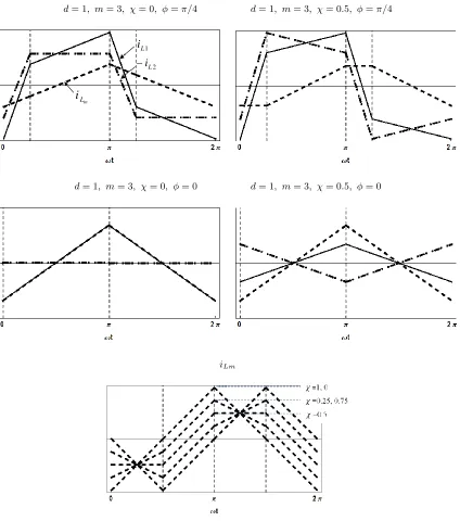
The equations of line current and the amount of power transfer with a finite magnetizing inductance are a function ofχand m. As can be expected intuitively, the derived equations in Eq 2.23 ∼ Eq 2.26 become the same as equations Eq 2.3 ∼ Eq 2.7 with m going to infinity. Additionally,Po Lm becomes the same asPo whenχis zero or unity as seen in the scaling factor and Fig 2.26. When the system is symmetric (χ=0.5), the effect of magnetizing inductance is maximized as shown in Fig. 2.11. Theoretically, there is no impact on power transfer by the magnetizing inductance, regardless of its value, when any of the ports does not have a series inductance value.
Conventional transformers are generally built in a symmetric manner so that the case when
χ=0.5 has been considered in order to understand the impact of the magnetizing inductance of the transformers. However, the coaxial winding transformer (CWT) or ICWT have a con-siderably different structure and impedance matrix, so it is worth recognizing the effect of the magnetizing inductance with system symmetry in the case where the magnetizing inductance is considerable compared to the series inductance Ls.
The influence on the soft switching region with an asymmetric impedance matrix The total series inductance valueLs, which is the sum ofL1andL2, has to be in a certain range
k
Figure 2.12: ZVS region with k,χ andm
primary and the secondary sides is derived in the same manner from the mirrored waveform of steady state operation . The initial inductance current values are obtained in Eq 2.27.
iL11(0) =
πVi(χ−1 + (k−1)m) 2ωLs(m+χ−χ2)
, iL12(φ) =
πVi(kχ+ (k−1)m) 2ωLs(m+χ−χ2)
(2.27) The condition for the devices to stay in the ZVS region with phase shift modulation is: For leading bridge : iL1[0]≤0,
χ−1 + (k−1)m
(m+χ−χ2) <0 (2.28)
For lagging bridge : iL1[θps]≥0,
kχ+ (k−1)m
(m+χ−χ2) >0 (2.29)
be ideal switches.
d= 1, m= 3, χ= 0, φ=π/4 d= 1, m= 3, χ= 0.5, φ=π/4
m
L i
1 L i
2 L
i
d= 1, m= 3, χ= 0, φ= 0 d= 1, m= 3, χ= 0.5, φ= 0
iLm
2.3
Three-phase dual-active bridge converter topology - Yy
connection
The three-phase DAB DC/DC converters previously introduced are conventionally configured in a three-phase Yy connection as shown in Fig 2.14. The three-phase DAB DC/DC converters have the advantage with a lower VA rating and stress on circuit components, in exchange for requiring a high number of power devices when compared to single-phase DAB DC/DC converter topology.
2.3.1 Steady state lossless operation Three phase Yy connection
The approach to deriving inductance current and design parameters is the same as with single-phase DAB DC/DC converter applications. There are a total of six modes for two distinct regions of operation between 0 ≤ θps < π/3 and π/3 ≤θps < π/2. The transition of the line current between modes is more sinusoidal than that of the single phase DAB operation.
Six modes of operation with phase-shift modulation are identified for each operating regions, and equations are derived in Appendix B. The amount of power transfer with phase-shift modulation in a three-phase DAB DC/DC converter in Yy connection is shown in Eq 2.30.
AC-Link
HV side LV side
Figure 2.14: Three-phase DAB DC/DC converter topology in Yy connection
(
Po Y y = kV2
1DC(4π−3θps)θps
6ωLsπ , for 0≤θps<
π
3
= kV
2 1DC(π
2−18π+18θ2
ps)
18ωLsπ , for
π
3 ≤θps <
π
2
2.24 0.50
Figure 2.15: Waveforms of a three-phase DAB DC/DC converter in Yy connection
iL1Y y rms= V1DC
√
5(k−1)2π3+54kπθ2
ps−27kθps3
9√3πωLs , for 0
≤θps< π3 = V1DC
√
(5−9k+5k2)π3−9kπ2θ
ps+81kπθps2 −54kθps3
9√3πωLs , for
π
3 ≤θps <
π
2
(2.31)
where iL1rms=iA rms =nia rms
v1Y y rms and v2Y y rmsof the three-phase converter are represented by:
v1Y y rms=
√
2
3 V1DC, , v2rms =n
√
2
3 V2DC (2.32)
Hence, the VA rating of the transformer is shown in Eq 2.33.
TV A Y y=
v1rms·i1rms+v2rms·i2rms
2 =
(1 +k)v1rms·i1rms
2 (2.33)
Po single phase|θps=π2
Po Y y|θps=π2
= 9
7 (2.34)
The inductance value per phase of a three-phase transformer in Yy connection should be scaled down by a factor of 79 to achieve the same amount of maximum power transfer with a single-phase DAB DC/DC converter. Hence, the base numbers for a three-phase DAB DC/DC converter in Yy connection are:
Vb Y y =V1DC, Ib Y y = 9 7
Vb
ωL, PbY y =VbIb. (2.35)
0 Π
2 Π
3Π 2
2Π
0 Æ
(a)θps= 0◦, k= 1
0 Π
2 Π
3Π 2
2Π
0 Æ
(b)θps= 25◦, k= 1
0 Π
2 Π
3Π 2
2Π
0 Æ
(c)θps= 50◦, k= 1 Figure 2.16: Line current waveforms of single phase DAB converters
2.3.2 Soft switching scheme - Three phase Yy connection
For the leading bridge :iL1[0]≤0, (
k≤ 7(2π18−π3θ
ps), for 0≤θps <
π
3
k≤ 9(2π−3θps)
14π , for
π
3 ≤θps<
π
2
(2.36)
For the lagging bridge :iL1[θps]≥0,
(
k≤ 7(π−6π2θ
ps), for 0≤θps <
π
3
k≤ 27(π−2θps)
14π , for
π
3 ≤θps<
π
2
(2.37)
The real and apparent power transfer, with soft switching boundaries, of the three-phase DAB DC/DC converter in a Yy connection is shown in Fig 2.17 in the same manner as it was for single-phase DAB applications.
0 Π 4 Π 2 10 Π 4 Π 2 1 0 Π 4 Π 2 10 Π 4 Π 2 1
Figure 2.17: Real and average apparent power with θps and k (Black line : Soft switching boundary)
2.4
Summary
Chapter 3
MEDIUM-FREQUENCY AND
MEDIUM-VOLTAGE COAXIAL
WINDING TRANSFORMER
There are many high frequency transformers used commercially in the range of several hundreds of kHz for low voltage switching mode power electronics applications. However, grid connected transformers are the same physical transformers, based on electromagnetic induction at 60Hz line frequency, that have been used since the 1900’s. As solid-state transformers and a variety of high frequency materials are introduced, a lot of attention has been drawn to MF/MV transformers to replace conventional line transformers for power electronics applications.
The advent of solid sate transformer applications does not mean that electromagnetic induction-based transformers will be eliminated by solid-state circuit elements. The galvanic isolation by electromagnetic induction of transformers cannot be replaced by electronic circuit components at the medium voltage level as of yet. Isolation protection is necessary for a grid voltage level to protect against electric shock and comply with strictly observed international standards. Besides that, the high conversion ratio between grid and end users is still hard achieve with only switching operation at an acceptable efficiency. Therefore, a high frequency isolation transformer is still a critical part in solid-sate transformer applications, and increas-ing the operatincreas-ing frequency of isolation transformers in medium-voltage level is an emergincreas-ing research area.
In practice, devolvement and testing of MV/MF transformers in the range of several kV at several tens’s of kHz in a college facility is a truly challenging task. Designing transformers at a medium-voltage level not only requires strong technical knowledge and experience, but also elaborate manufacturing facilities that include winding, insulation in packaging capabilities.