This paper is a postprint of a paper submitted to and accepted for publication in IET Renewable Power Generation and is subject to Institution of Engineering and Technology Copyright. The copy of record is available at IET Digital Library
A single-stage ac-dc buck-boost converter for medium-voltage high-power
applications
I. Abdelsalam1,2, G.P. Adam1,D. Holliday1and B.W. Williams1
Electronic and Electrical Engineering Department, University of Strathclyde, Glasgow, UK1
Electrical Power Department, Arab Academy for Science and Technology and Maritime Transport, Cairo, Egypt2
Email: [email protected] and [email protected].
Abstract ─This paper proposes three topologies based on single-stage three-phase ac-dc buck-boost converters suitable for medium-voltage high-power applications. The first two topologies are based on a dual three-phase
buck-boost converter, with a three-winding phase-shifted transformer to achieve sinusoidal input currents, with
relatively small ac filters. The limitation of these two topologies are the switching devices are exposed either to
a high voltage beyond that tolerable by a single device. The third topology is based on three single-phase buck-
boost converters; with their dc output terminals connected in series to generate high voltage. By using this
approach, voltage stresses on the switching devices are greatly reduced, and sinusoidal input currents with
nearly unity power factor is achieved over the entire operating range when using small ac filters. Analysis,
PSCAD/EMTDC simulations and experimentation are used to assess the feasibility of the proposed topologies
during normal operation. Major findings of this study are discussed and summarised as a comparison between
the three topologies.
Key words: ac-dc converters, buck-boost converters, wind energy conversion system and back-to-back
converters
I.
I
NTRODUCTION
AC-dc converters are used intensively as back-to-back converters in renewable energy systems such as wind and
solar; dc-motor drives and dc distributed generation systems (micro-grids); and in power supplies for industrial
and domestic electric appliances. Utility recognition of ac-dc conversion power quality problems, especially,
harmonic currents injected into ac side, has meant practical measures are taken to improve the power factor and
quality of the ac grid currents of these converters. Also, effort is being invested to develop new generations of
ac-dc converters that can meet strict power quality regulations and offer the flexibilities needed in renewable
power conversion systems[1-5]. Generally, three-phase ac-dc converters can be categorised as follows: buck,
boost, and buck-boost converters, and single-stage and two-stage converters. In the majority of the two-stage
diodes Dbd1 and Dbd2. Both topologies ‘A’ and ‘B’ exploit the harmonic cancelation feature of the three-phase
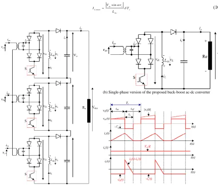
three windings phase-shifted transformer to decrease the size of the ac side C-filter needed to produce high quality input currents. The third topology proposed in this paper is topology ‘C’, which consists of three single-phase buck-boost converters with dc outputs connected in series as shown in Fig. 2(a). Each sub-converter is rated at ⅓ the total converter rated power and the voltage stress per switch is reduce to the line-to-neutral voltage plus ⅓ the output voltage. Although topology ‘C’ can operate under continuous or discontinuous dc-link inductance current modes (CCM or DCM), simulation studies show that DCM is better as it reduces the voltage stress on the main switching device and the blocking diode in each sub-converter. This is achieved with higher current stresses in these devices compared to CCM.
The three proposed topologies have the following features: buck and boost capability in a single stage with a minimum switch count, modular structure, simple control system, and sinusoidal supply current with unity power factor.
This paper is organised as follows: Section II describes the operating principle of the proposed dual three-phase ac–dc buck–boost converters (topologies ‘A’ and ‘B’), including their control loop systems and filter design. Section III describes the operating principle of topology ‘C’, and establishes the basic equations that govern its steady-state operation under CCM and DCM. Its control loops are defined. Section IV uses simulation results from PSCAD/EMTDC to demonstrate the technical feasibility of topologies ‘B’ and ‘C’ (under CCM and DCM), including a comparison between topologies ‘B’ and ‘C’. Section V presents experimental results from a 10kW prototype of topology ‘C’ to verify its steady state and dynamic performance during DCM operation. Conclusions and major findings are highlighted in Section VI.
II.
D
UAL THREE
-
PHASE BUCK
-
BOOST CONVERTER TOPOLOGIES
‘A’
AND
‘B’
a) Circuit description
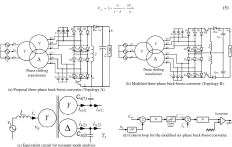
Fig.1(a) shows a medium-voltage high-power dual three-phase buck-boost converter (topology ‘A’), which is an improved version of the single and three-phase buck-boost converters discussed in [17]. It consists of two cascaded three-phase diode bridges and series commutable switch ‘S’, see Fig.1(a). Switch ‘S’ is used to control
the output dc voltage by modulating inductor current IL. Turning on switch ‘S’ boosts the energy stored in dc
inductor Ldc, and this stored energy supplies the load when switch ‘S’ is off. The proposed converter uses a three
winding transformer, with secondary and tertiary windings are phase shifted 30o (Δ/Y) from each other to attenuate the 5th and 7th harmonic currents. The ac filters (Cs) connected to transformer secondary and tertiary
associated with the switching frequency components and their sidebands. To simplify the analysis, the rated rms line-to-line voltage of all windings are assumed equal, vp=vs1=vs2; this means the transformer turns ratios are N1/N2=1 (for the star secondary) and N1/N3=1/√3(for the delta secondary). The average output voltage of each
bridge rectifier is −3√3π 𝑉𝐶𝑚, where Vcm is the peak fundamental ac voltage across the filter capacitor Cs. The
negative sign reflects the inversion of the bridge output voltage with respect to the load. By using the approach described in [17, 19, 20], the average output dc voltage Vdc in CCM is:
3 3
2 1
d c c m
V V
(1)
where δ represents the duty cycle of the switch ‘S’. By controlling δ over a wide range 0<δ<1, buck (δ<½) and boost (δ>½) operation can be achieved. The major shortcoming of the converter in Fig.1 (a) is that the blocking diode Dbd and switch S are exposed to extremity high voltage stresses of Vdc+2VCm. This may limit use of the
proposed buck-boost converter to the lower end of medium-voltage applications. Topology ‘B’ is proposed as shown in Fig.1(b), which is an improved version of the converter in Fig.1 (a), where the problem of voltage stresses are partially solved by using two switching devices S1 and S2 and two blocking diodes Dbd1 and Dbd2 to
evenly share the overall voltage stress. This is achieved by splitting the dc inductance Ldc into Ldc1 and Ldc2
(where Ldc1=Ldc2=¼Ldc), and the two dc side capacitors (Cdc1=Cdc2) are connected as Fig.1(b). Although
topology ‘B’ is slightly changed from topology ‘A’, it still maintains the simplicity and performance of the original circuit, and switches S1and S2 receive identical gating signals.
b) Filter design and power factor performance
Fig.1(c) shows the equivalent circuit for resonant mode analysis, and filter admittance can written in terms of filter capacitance and transformer inductances as:
2
1 ( )
1
1
1 s
r
s
s r s
Y s s C
s L
s C
s L s L C
(2)
where Ls is the transformer primary leakage inductance plus the inductance of the supply lines, and Lr is the
transformer secondary and tertiary leakage inductances. It is possible to make the leakage inductances of the Y and ∆ transformer equal [21]. The parallel resonant frequency can be calculated from the zeros of the Y(s)
admittance:
1 1
r s L C
2
1
2Ls Lr Cs
(4)
The transformer is used to cancel the 5th, 7th, 17th, and 19th harmonic currents [22-24], and1depends on the
transformer secondary leakage inductance. Since the transformer leakage inductances are known, the value of the ac-side C-filter is selected such that the cut-off frequency is placed at nine times the base frequency, 9ωB.
With the ac filter designed on this basis, simulation studies show that acceptable supply current THD is achieved over the full control range.
c) Control strategy
Fig.1(d) summarises the control scheme used to control the dual three-phase buck-boost converters in Fig.1(a) and (b). The control system in Fig.1(d) consists of an outer voltage loop that controls the converter total output dc voltage (Vdc) and sets reference inductor current (𝐼𝐿∗); and an inner current loop that forces the dc inductor
current IL to follow its reference, and generates duty cycle δ for the switch S or (S1 and S2). The output of the
second proportional-integral (PI) controller is compared with a triangular carrier wave to generate the gating signal with fixed pulse width for given operating point to control the buck-boost converter switch (S) or switches (S1and S2). Operation of switch S with fixed pulse width allows the converter output dc voltage to be
controlled, but does not improve the harmonic attenuate of the input ac currents due to discontinuity of the input currents caused by the 120o conduction pattern of the diode rectifier bridges [17].
III.
THREE
-
PHASE BUCK
-
BOOST CONVERTER TOPOLOGY
‘C’
a) Circuit description
To further reduce the voltage stresses on the semiconductor devices, the three-phase buck-boost converter proposed in Fig. 2 (a) is proposed, Topology ‘C’ which uses each single-phase diode bridge in series with a switch. The ac terminals of the diode bridge of each phase are connected to three single-phase transformers with isolated secondary windings, while the primary sides can be connected star or delta; however, star connection is shown in Fig. 2 (a). The co-existence of each diode bridge in series with an active switch allows the proposed converter to regulate its dc output voltage in buck and boost mode, with reduced voltage stress per active switch (S1, S2 and S3) and blocking diode (Dbd1, Dbd2 and Dbd3): reduced to the line-to-neutral voltage plus ⅓ theoutput
2 3
1
m d c
V
V
(5)
(a) Proposal three-phase buck-boost converter (Topology A).
(b) Modified three-phase buck-boost converter (Topology B).
(c) Equivalent circuit for resonant mode analysis.
[image:6.595.65.530.68.362.2](d) Control loop for the modified six-phase buck-boost converter.
Fig.1: Three-phase dual buck-boost converters and their control systems.
b) DCM analysis
For simplicity, the analysis of the proposed converter during DCM operation is carried out on per phase basis, and then extended to the three-phase version. Per phase analysis of the output dc voltage of a single-phase full-bridge diode is adopted.
Assume the switching and supply fundamental frequencies are fs and f, during the analysis of each switch period
the supply voltage is assumed fixed, and the voltage drop in the series elements of input L-C filter is assumed to be sufficiently small to be neglectable. Fig. 2(c) shows that the ac-dc buck-boost converter being studied has three operating intervals in DCM:
First interval (0<t<ton): This mode represents the situation when the switch S is on and the dc-link inductor Ldc
is being energised from the supply, and dc-side capacitor supplies the load with near constant current if its capacitance is sufficiently large. In this interval, the dc-link inductor voltage and current, and dc capacitor current are:
( ) ( ) s in
L s s m s
v t v t V t (6)
s i n
( ) m s
L
d c
V t
d i t
d t L
( ) o
c
V i t
R
(8)
After solving these equations, iL(t) in this interval is:
s i n
( ) m s
L
d c
V t
i t t
L
(9)
With switching frequency fs selected to be much higher than supply frequency f, equation 10 can be used to
approximate the peak inductor current (ILmax) at the instant when the switch S is turned off (at t= ton=δTs).
m a x s in
m s
L s
d c
V t
I T
L
(10)
(a) Proposed three-phase buck-boost converter (topology C).
(b) Single-phase version of the proposed buck-boost ac-dc converter
(c) Waveforms: voltage across dc-side inductor vL, inductor current iL,
output current io and dc-side capacitor current over two and half switching
[image:7.595.70.516.256.634.2]cycles (for one phase Fig. 2 (b)).
Fig. 2: Proposed three-phase ac-dc buck-boost converter.
negative polarity as shown in Fig. 2 (c). Thus, the dc-link inductor voltage and current, and dc capacitor current are:
( )
L o
v t V (11)
m a x
s i n ( )
( ) ( ) ( ) m s
o o o
L
L o n L s s
d c d c d c d c
V t
V V V
d i t
i t t t I t T T
d t L L L L
(12)
s i n
( ) ( ) ( ) o ( ) m s o
c L o s s
d c d c
V t
V V
i t i t i t t T T
L L R
(13)
From Fig. 2 (c),iL(ton+tx)=0 when the energy stored in the dc link inductor Ldc is exhausted; thus, tx is:
s i n ( )
m s x s o V t t T V (14)
Alternatively, this equation can be obtained by setting the average dc link inductor voltage to zero.
Third interval (ton+tx< t ≤Ts): This interval represents the period when the energy stored in the dc link inductor
Ldc is fully exhausted when its current drops to zero at t=ton+tx before the next switching period and remains at
zero. In this interval, inductor current and voltage are iL(t)=0 and vL(t)=0, and the dc link capacitor current is:
( ) o
c o
V
i t i
R
(15)
Considering the three intervals, the average capacitor current during one switching cycle is:
𝑖
̅ =
𝑐 1𝑇𝑠
[∫
𝑖
𝑐(𝑡)𝑑𝑡 + ∫
𝑖
𝑐(𝑡)𝑑𝑡 +
𝑡𝑜𝑛+𝑡𝑥
𝑡𝑜𝑛
∫
𝑖
𝑐(𝑡)𝑑𝑡
𝑇𝑠
𝑡𝑜𝑛+𝑡𝑥
𝑡𝑜𝑛
0
] =
−
𝑉𝑜𝑅
−
½𝑉𝑜𝑡𝑥2+𝑉𝑜𝑡𝑜𝑛𝑡𝑥−𝑉𝑜𝛿𝑇𝑠𝑡𝑥−|𝑉𝑚 sin 𝜔𝑡𝑠|𝛿𝑇𝑠𝑡𝑥
𝐿𝑑𝑐𝑇𝑠
(16)
Since the input current and output dc voltage of a single-phase full-bridge diode rectifier have half wave symmetry (0<ωt<π), the average capacitor current during one half of the supply cycle is:
𝑖𝐶_𝐻𝐶
̅̅̅̅̅̅ =1
𝜋∫ (−
𝑉𝑜
𝑅− 1
𝐿𝑑𝑐𝑇𝑠[½𝑉𝑜𝑡𝑥
2+ 𝑉
𝑜𝑡𝑜𝑛𝑡𝑥− 𝑉𝑜𝛿𝑇𝑠𝑡𝑥− |𝑉𝑚sin 𝜔𝑡𝑠|𝛿𝑇𝑠𝑡𝑠]) 𝑑𝜔𝑡𝑠
𝜋
0 (17)
2 2 _
4
s m o
c H C
d c o
T V V
i
L V R
(18) The steady state average capacitor current tends to zero; the converter voltage gain can be calculated as:
1 0 2
s d c
T R
V V m
L
For a given dc link inductance Ldc, the critical duty cycle δc that defines the boundary between CCM and DCM
can be obtained by setting tx=Toff=(1-δc)Ts and |Vmsinωts|=Vm. From equations (14) and (19) δc is:
2 1 s c d c T R L
(20)
In each switching period during DCM operation, the equivalent continuous current in the switch S and pre-filter input current are:
2
1
( ) s in , 0
2
S s m
i t T V t t
L (21) 2 1
( ) s in , 0 2
2
r s m
i t T V t t
L
(22)
Equation (21) represent the equivalent continuous current in switch S, and (22) represents the fundamental component of the pre-filter input current, which is sinusoidal and in-phase with the supply voltage. Since the switched version of the input current isr(t) is contained within the envelope of the supply voltage, isr(t) only
contains switching frequency harmonic components and their sidebands. This feature makes the ac-side L-C filter size smaller and simpler in design than that of the dual three-phase buck-boost converter discussed. These observations indicate that with a small ac filter and fixed duty cycle, the input current of the three-phase buck-boost converter in Fig. 2 (a) can be ensured to be sinusoidal (as there are no low-order harmonics to distort the input current).
The average and root mean square current in the switch S are:
𝐼̅ =𝑆 1𝜋∫ 𝛿
2𝑇𝑠𝑉𝑏sin𝜔𝑡
2𝐿𝑑𝑐
𝜋
0 𝑑𝜔𝑡 =
𝛿2𝑇 𝑠𝑉𝑚
𝜋𝐿𝑑𝑐 (23)
𝐼𝑆_𝑟𝑚𝑠 = √1𝜋∫ 𝛿
4𝑇𝑠2𝑉𝑚2sin𝜔𝑡
4𝐿2𝑑𝑐 𝜋
0 𝑑𝜔𝑡=
𝛿2𝑇𝑠𝑉𝑚
2√2𝐿𝑑𝑐 (24)
The average and root mean square current in each diode of the single-phase bridge are:
𝐼̅ =𝐷 2𝜋1∫ 𝛿
2𝑇𝑠𝑉𝑚sin 𝜔𝑡
2𝐿𝑑𝑐
𝜋
0 𝑑𝜔𝑡 =
𝛿2𝑇𝑠𝑉𝑚
2𝜋𝐿𝑑𝑐 (25)
𝐼𝐷_𝑟𝑚𝑠= √2𝜋1 ∫ 𝛿
2𝑇𝑠2𝑉𝑚2sin 𝜔𝑡
4𝐿𝑑𝑐2
𝜋
0 𝑑𝜔𝑡 =
𝛿2𝑇𝑠𝑉𝑚
4𝐿𝑑𝑐 (26)
3 0 _ 3 2
3
s
p h
d c
T R
V V m
L
(27)
3 _ 1 2
3
s c r p h
d c T R L
(28)
c) Control strategy
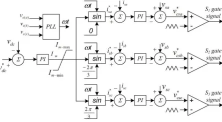
Fig. 3(a) shows the proposed controller for the converter in Fig. 2(a) under CCM, where there is one outer control loop and three inner control loops (one per phase). The outer control loop regulates the converter dc output voltage and estimates the peak fundamental current im required to maintain the dc link voltage at any
desired level. The inner control loops provide reference currents (𝑖𝑠𝑎 ∗ ,𝑖𝑠𝑏 ∗ ,𝑖𝑠𝑐 ∗ ) synchronised to the grid voltage, see Fig. 3(a). In addition, to ensuring sinusoidal input currents independent of the load conditions, these inner control loops estimate the fundamental component of the ac side capacitor voltages (𝑣𝑐𝑠𝑎∗ , 𝑣𝑐𝑠𝑏∗ , 𝑣𝑐𝑠𝑐∗ ) required to force the input current to follow its control reference (𝑖𝑠𝑎 ∗ ,𝑖𝑠𝑏 ∗ ,𝑖𝑠𝑐 ∗ ) and ensure power balance between the ac and dc sides.
Fig. 3(b) summarises the control structure used to control the proposed converter in Fig. 2(a) under DCM operation, which consists of inner and outer control loops. The outer control loop regulates the total output dc voltage Vdc, where a PI controller estimates the reference peak fundamental supply current I
*
p to achieve any
desired dc link voltage Vdc, a current limiter is added in the outer control loop to protect the converter from over
load. The inner loop forces the peak of the supply current to follow its reference set by the outer loop and estimates the duty cycle δ of switch S.
(a) Proposed controller for CCM operation
[image:10.595.188.410.504.626.2] [image:10.595.183.410.663.708.2]IV.
SIMULATION RESULTS
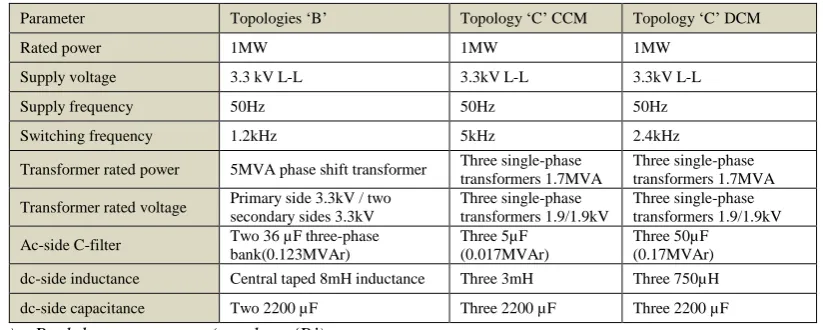
[image:11.595.91.503.301.466.2]This section presents simulation results obtained from PSCAD/EMTDC models of the proposed buck-boost converters topologies. This simulation section consists of four parts. The first part shows the closed loop results of the proposed converter shown in Fig.1(b), while the second and the third parts show the simulation results of the proposed converter shown Fig. 2(a) under CCM and DCM respectively. The converter parameters are listed in Table 1. To highlight the features of the proposed converters, they are simulated under the same operating scenarios. Initially, the dc voltage across a 150Ω load resistance is set to 10kV. At time t=0.75s, the load resistance reduced to 100 Ω to test the dynamic response of both converters.
Table 1: Simulation parameters of the three buck-boost converter topologies presented in Fig.1(b) and Fig. 2(a).
Parameter Topologies ‘B’ Topology ‘C’ CCM Topology ‘C’ DCM
Rated power 1MW 1MW 1MW
Supply voltage 3.3 kV L-L 3.3kV L-L 3.3kV L-L
Supply frequency 50Hz 50Hz 50Hz
Switching frequency 1.2kHz 5kHz 2.4kHz
Transformer rated power 5MVA phase shift transformer Three single-phase
transformers 1.7MVA
Three single-phase transformers 1.7MVA
Transformer rated voltage Primary side 3.3kV / two secondary sides 3.3kV Three single-phase transformers 1.9/1.9kV Three single-phase transformers 1.9/1.9kV
Ac-side C-filter Two 36 µF three-phase
bank(0.123MVAr)
Three 5µF (0.017MVAr)
Three 50µF (0.17MVAr)
dc-side inductance Central taped 8mH inductance Three 3mH Three 750µH
dc-side capacitance Two 2200 µF Three 2200 µF Three 2200 µF
a) Buck-boost converter (topology ‘B’)
The simulation results for topology ‘B’ are shown in Fig. 5. The transformer primary side inductance plus the supply inductance is 0.15pu, and the secondary leakage inductance is 0.1 pu for each winding. The ac-side C-filter value is selected such that the cut-off frequency is nine times the base frequency (9ωB), according to
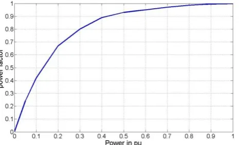
Fig. 4: Power factor profile of topologies ‘A’ and ‘B’
Fig. 5(a) show that the proposal converter is able to track the reference output voltage, with minimum overshoot when the load resistance is halved. Fig. 5(b) shows the three-phase supply currents and phase ‘a’ voltage during
the step increase in load. From Fig. 5 (b) the proposed converter draws sinusoidal current from the supply, with 0.935 power factor leading in case 1 and unity power factor when the load resistance decreases to 100. The switch S is exposed to a voltage stress of 10kV approximately; see Fig. 5(c). Fig. 5(d) shows the dc-link inductor current where the current increases to compensate the step load change
b) Buck-boost converter (topology ‘C’) in CCM
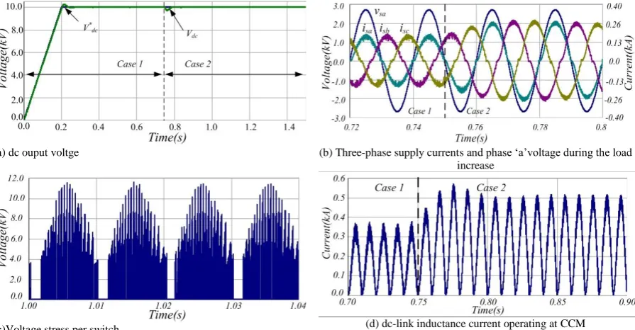
The closed loop results of the converter shown in Fig. 2(a) under CCM conditions are shown in Fig. 6. Fig. 6(a) shows the proposed converter is able to force its dc output voltage to follow the reference voltage in buck and boost modes, including when the load resistance is decreased from 150Ω to 100 Ω. The under-shoot observed in Fig. 6(a) takes longer to be corrected, due to the large dc side inductances needed for CCM. These inductors do not allow rapid dc current change; thus, produce a slowed dynamic performance compared to the DCM case to be presented in the following subsection. Fig. 6(b) shows samples of the three-phase current inputs and phase ‘a’ voltage, all zoomed around the instant when the load resistance changes. Fig. 6(c) shows a sample of the
voltage stress across the switch S1. The voltage stress across this switch is comparable to the theoretical value
(a) dc-output voltage. (b) Three-phase supply currents and phase ‘a
’voltge during a load increase
[image:13.595.74.523.67.295.2](c) Voltage stress per switch. (d) dc-link inductance current.
Fig. 5: Simulation results for the proposed six-phase buck-boost converter.
(a) dc ouput voltge (b) Three-phase supply currents and phase ‘a’voltage during the load
increase
(c)Voltage stress per switch. (d) dc-link inductance current operating at CCM
Fig. 6 Simulations illustrate the performance of the proposed three-phase buck-boost converter (topology ‘C’) under CCM.
c) Buck-boost converter (topology C) under DCM operating conditions
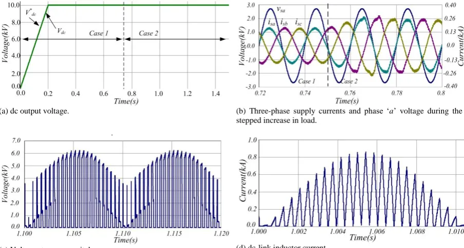
[image:13.595.77.525.329.562.2]III. Fig. 7(d) shows a zoomed version of the dc-link inductor current, and the converter is seen to operate on boundary between CCM and DCM.
(a) dc output voltage. (b) Three-phase supply currents and phase ‘a’ voltage during the
stepped increase in load.
Stres s
[image:14.595.73.525.118.360.2](c) Voltage stress per switch. (d) dc-link inductor current.
Fig. 7: Simulation results of the perofrmance of the three-phase buck-boost converter under DCM.
d) Comparison between the proposed buck-boost converters in Fig.1 (a) and Fig. 2 (a)
The three-phase converter under DCM has a faster dynamic response due to using smaller dc-side inductance and a medium size ac-side C-filter, see Fig. 5(a), Fig. 6(a) and Fig. 7 (a)
Sinusoidal current with near unity pf is achieved with topology ‘C’ in both CDM and DCM modes, over a wide range of operating conditions. This is unlike the dual three-phase buck-boost converters in Fig. 1(a) and (b) that ensure nearly unity power factor over a limited range according to a pre-defined profile.
Topology ‘C’ under DCM has lower semiconductor voltage stress, but the highest current stress per switch.
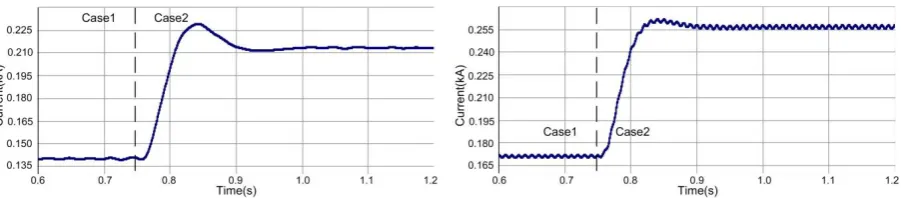
For the same supply voltage and rated output power, the three-phase buck-boost converter (topologies ‘A’ and ‘B’) have the lowest average dc-link inductor current as shown in Fig.8. This is because their rectified dc output voltages are higher than that of the three series connected single phase case, by a factor of √23 .
as an interfacing converter for permanent magnetic wind-turbine generators, and for operation as a front-end converter for grid-connected current and voltage source converters, with black-start and shutdown capabilities. Also the modified dual three-phase buck-boost converter (Topology ‘B’) has the advantage of lower current stress per device, and the three-phase buck-boost converters under DCM (Topology ‘C’) has the advantages of lower voltage stress per switch and lower supply current THD.
[image:15.595.77.528.184.283.2](a) Average dc-link inductor current of topology ‘B’. (b) Average dc-link inductor current of topology ‘C’
Fig.8: Average dc-link inductor current.
V.
EXPERIMENTAL RESULTS
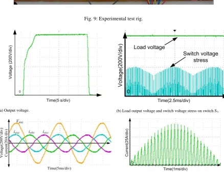
A 10kW prototype of the proposed three-phase buck-boost converter (topology ‘C’, see Fig. 9) was assessed to establish its steady state and dynamic performance during DCM operation, with system parameters listed in Table 2. To demonstrate the soft start and shut-down capability, the output dc link voltage (Vdco) is increased
from 0 to 1250V and then reduce to zero within 30s. The results are displayed in Fig. 10. From Fig. 10(a) the proposed converter provides high boost with good dynamic response during soft start up, steady state and shutdown. Fig. 10 (b) shows the steady state output voltage and the voltage stress across switch S, where the voltage stress across the switch is 600V, as expected ( 1
3
1 3 0 2 1 2 5 06 0 0V, which is much lower than in topologies A and B). Fig. 10(c) shows that the supply current is sinusoidal with nearly unity power factor (this is achieved without any dedicated control to force unity power factor operation). The dc-side inductor current (iL)
in Fig. 10(d) confirms DCM operation of the proposed buck-boost converter.
Table 2 Experimental setup parameters.
Parameter Value
Supply voltage 260VL_N
Transformer rated power 8kVA
Transformer rated voltage 440/220VL-L
ac-side capacitance 80µF
dc-side inductance 330 µH
Fig. 9: Experimental test rig.
(a) Output voltage. (b) Load output voltage and switch voltage stress on switch S1.
[image:16.595.75.514.240.581.2](c) Three-phase supply currents and phase ‘a’ voltge at steady state. (d) dc-link inductor current.
Fig. 10: Waveforms showing the overall performance of the proposed three-phase buck-boost converter.
VI.
C
ONCLUSION
blocking diodes and switch S. Also, it has better harmonic performance and input power factor profile, from no-load to full-no-load conditions, than topologies ‘A’ and ‘B’. But the switching devices are exposure to higher current stresses. The theory, simulations, and experimental results presented establish that the proposed ac-dc buck-boost converters are viable for medium-voltage, high-power, ac-dc conversion applications, including grid interfacing of wind energy systems.
VII.
R
EFERENCES
[1] G. K. Andersen and F. Blaabjerg, "Current programmed control of a single-phase two-switch buck-boost power factor correction circuit," Industrial Electronics, IEEE Transactions on, vol. 53, pp. 263-271, 2006.
[2] F. Q. Wang, H. Zhang, and X. K. Ma, "Intermediate-scale instability in two-stage power-factor correction converters," Power Electronics, IET, vol. 3, pp. 438-445, 2010.
[3] A. El Aroudi, M. Orabi, R. Haroun, and L. Martinez-Salamero, "Asymptotic Slow-Scale Stability Boundary of PFC AC–DC Power Converters: Theoretical Prediction and Experimental Validation,"
Industrial Electronics, IEEE Transactions on, vol. 58, pp. 3448-3460, 2011.
[4] L. Yu-Kang, Y. Shang-Chin, and L. Chung-Yi, "A High-Efficiency AC-to-DC Adaptor With a Low Standby Power Consumption," Industrial Electronics, IEEE Transactions on, vol. 55, pp. 963-965, 2008.
[5] M. I. Marei, I. Abdallah, and H. Ashour, "Transformerless uninterruptible power supply with reduced power device count," Electric Power Components and Systems, vol. 39, pp. 1097-1116, 2011.
[6] Y. Jang and R. W. Erickson, "New single-switch three-phase high-power-factor rectifiers using multiresonant zero-current switching," Power Electronics, IEEE Transactions on, vol. 13, pp. 194-201, 1998.
[7] E. H. Ismail and R. Erickson, "Single-switch 3φ PWM low harmonic rectifiers," Power Electronics,
IEEE Transactions on, vol. 11, pp. 338-346, 1996.
[8] S. K. Bassan, D. S. Wijeratne, and G. Moschopoulos, "A Three-Phase Reduced-Switch High-Power-Factor Buck-Type Converter," Power Electronics, IEEE Transactions on, vol. 25, pp. 2772-2785, 2010.
[9] R. L. Alves and I. Barbi, "Analysis and Implementation of a Hybrid High-Power-Factor Three-Phase Unidirectional Rectifier," Power Electronics, IEEE Transactions on, vol. 24, pp. 632-640, 2009. [10] C. Jui-Yuan, C. Yuan-Chih, and L. Chang-Ming, "On the Switched-Reluctance Motor Drive With
Three-Phase Single-Switch Switch-Mode Rectifier Front-End," Power Electronics, IEEE Transactions on, vol. 25, pp. 1135-1148, 2010.
[11] Y. Kai, R. Xinbo, Z. Chi, and Y. Zhihong, "Three-phase single-switch boost PFC converter with high input power factor," in Energy Conversion Congress and Exposition (ECCE), 2010 IEEE, 2010, pp. 2921-2928.
[12] J. Yu Lin, "Single switch three-phase ac to dc converter with reduced voltage stress and current total harmonic distortion," Power Electronics, IET, vol. 7, pp. 1121-1126, 2014.
[13] S. Weiwei, L. Hui, and J. Jiuchun, "Analysis and implementation of instantaneous current control for multiple boost converter in WECS," in Applied Power Electronics Conference and Exposition, 2008.
APEC 2008. Twenty-Third Annual IEEE, 2008, pp. 1490-1495.
[14] S. Kim and P. N. Enjeti, "Control of multiple single-phase PFC modules with a single low-cost DSP,"
Industry Applications, IEEE Transactions on, vol. 39, pp. 1379-1385, 2003.
[15] J. Yungtaek and R. W. Erickson, "New single-switch three-phase high power factor rectifiers using multi-resonant zero current switching," presented at the Applied Power Electronics Conference and Exposition, 1994. APEC '94. Conference Proceedings 1994., Ninth Annual, 1994.
[16] J. Yungtaek and R. W. Erickson, "New single-switch three-phase high power factor rectifiers using multi-resonant zero current switching," in Applied Power Electronics Conference and Exposition,
1994. APEC '94. Conference Proceedings 1994., Ninth Annual, 1994, pp. 711-717 vol.2.
[17] I. Abdelsalam, G. P. Adam, D. Holliday, and B. W. Williams, "Three-phase ac–dc buck–boost converter with a reduced number of switches," IET Renewable Power Generation, 2015.
[18] D. Wijeratne and G. Moschopoulos, "A novel three-phase buck-boost ac-dc converter," in Applied
Power Electronics Conference and Exposition (APEC), 2011 Twenty-Sixth Annual IEEE, 2011, pp.
[19] I. Abdelsalam, G. P. Adam, D. Holliday, and B. W. Williams, "Single-stage, single-phase, ac–dc buck– boost converter for low-voltage applications," Power Electronics, IET, vol. 7, pp. 2496-2505, 2014. [20] H. Rashid, Power Electronics: Circuits, Devices, and Applications: Pearson/Prentice Hall, 2004. [21] X. Yuan, W. Bin, F. A. Dewinter, and R. Sotudeh, "A dual GTO current-source converter topology
with sinusoidal inputs for high-power applications," Industry Applications, IEEE Transactions on, vol. 34, pp. 878-884, 1998.
[22] B. Wu, High-power converters and AC drives: John Wiley & Sons, 2006.
[23] J. R. Rodriguez, J. W. Dixon, J. R. Espinoza, J. Pontt, and P. Lezana, "PWM regenerative rectifiers: state of the art," Industrial Electronics, IEEE Transactions on, vol. 52, pp. 5-22, 2005.