International Journal of Emerging Technology and Advanced Engineering
Website: www.ijetae.com (ISSN 2250-2459,ISO 9001:2008 Certified Journal, Volume 4, Issue 2, February 2014)
325
Grid Integration of AC and DC Energy Resources using
Multi-Input Nine Switch Matrix Converter
V. Kandasamy
1, R. Manoj
2Department of Electrical and Electronics Engineering, Kumaraguru College of Technology
Abstract—High penetration of Grid by various energy
resources leads to intermittent voltage and frequency variations. To smoothen out these variations and to integrate energy resources to the grid, this paper proposes a multi-input matrix converter topology to integrate the ac and dc energy resources to the grid. This matrix converter is based on the indirect matrix converter operating in the reverse boost mode. The reverse boost mode is preferred over the forward buck mode, since most of the energy resources have voltages lower than the grid voltage. The proposed matrix converter consists of nine switches providing six input terminals, there by a three phase AC source and three DC sources can be integrated to the grid. This proposed scheme guarantees sinusoidal input and output current waveforms and proper power dispatch to the grid.
Index Terms— Indirect Matrix Converter, Nine Switch Voltage Source Converter, Versatile Matrix Converter.
I.INTRODUCTION
Recent advancements in distributed generation and micro grids lead to integration of various energy resources and energy storages to utility grid. The ac energy sources include wind energy conversion system, diesel generator, micro turbines, flywheel energy storage system. The dc type includes photo voltaic(PV) panel, fuel cells and ultra capacitors. Among the above, renewable energy resources like photovoltaic, wind energy conversion systems are uncontrollable and outputs are influenced by environmental and weather conditions such as solar radiation, wind speed, etc. Numerous penetrations in the grid by various energy resources lead to voltage and frequency variations in the grid.
To smoothen these variations, the energy resources are integrated together, such that their characteristics complementing each other. Integrating resources together leads to higher certainty level and helps to meet better grid codes. Such integration can be done by using power converters. Each energy resource requires individual power converter and for latter, the sources share a common grid side inverter. Using individual power converter for each source may increase the semiconductor switch requirements and hence the cost. This also requires an electrolytic capacitor in the dc link which leads to problems of premature failure and increase in size of the conversion system.
In general, the dc-link capacitor is avoided by using a single stage indirect matrix converter(IMC), whose fictitious dc link makes it flexible for extension of topology. But the problem with the indirect matrix converter is its input-to-output gain is limited to 0.866. Hence IMC is not applicable for integration, as most of renewable energy resources have voltages lower than the grid voltage. So we propose here a versatile multi-input matrix converter which provides the following advantages.
Requirement of semiconductor switches for integration are reduced
If isolation is not a case of concern, passive step up transformer is not necessary for integration.
Near sinusoidal input and output and proper power dispatches
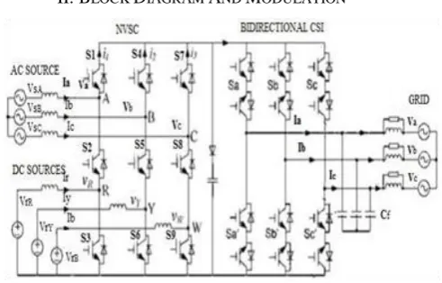
[image:1.595.316.562.429.586.2]II.BLOCK DIAGRAM AND MODULATION
Fig. 1. Block diagram of versatile matrix converter
A. Topology
International Journal of Emerging Technology and Advanced Engineering
Website: www.ijetae.com (ISSN 2250-2459,ISO 9001:2008 Certified Journal, Volume 4, Issue 2, February 2014)
The circuit comprises of a clamp circuit for safety reasons. The clamp circuit includes a diode and a small foil capacitor in series at the fictitious DC link.
B. Modulation of CSI.
[image:2.595.89.241.253.401.2]Theoretically, the output CSI can impose a selected line voltage across the dc link. The selection of voltage depends on the six active states and the three null states entering the CSI. The nine switching states of CSI are shown in the Fig. 2.
Fig 2. Space vector representation of CSI
The modulation index of the CSI cannot be varied for voltage boosting purposes, as the null states are not used. Only the ON switches of the active states are shown in figure. Considering the sextant 1(-π/6≤θ≤π/6) of CSI, voltage Vab or Vac is imposed on fictitious DC link,
depending on the active states entered.
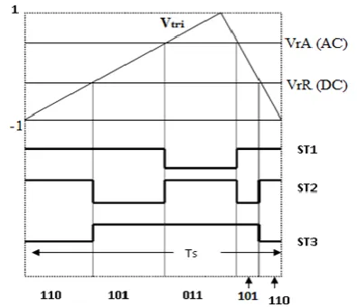
C. Modulation of NVSC
An ac modulating reference VrA and a dc modulating
reference VrR is needed for the modulation of NVSC. A
common triangular carrier wave Vtri is shared by both the
reference waves. It is necessary to vary the slope according to the state durations to produce the different dc link voltages applied across the NVSC. The variation in slope is directly proportional to duty ratios of the active states.
The switching states for the first leg of the NVSC are shown in Fig. 3. This relation can be expressed as
{
{
III.CONTROL ALGORITHM
The purpose of the control scheme is to ensure proper power dispatches to the grid with the help of modulation references. The implementation of the control schemes for generation of the references are explained below.
A. Control of NVSC ac Terminals
As the VMC do not have DC link capacitor unlike other usual matrix converter, it is not necessary to control the DC link. The power can be regulated in both input and output side. For the input side, the reactive power is set to zero, to achieve unity power factor. Similarly in grid side, the power factor angle ϕ is shifted to zero for unity power factor.
The block diagram for the NVSC ac source control is shown in Fig. 4. The phase angle θ is obtained from Phase Locked Loop(PLL) by sensing AC input voltages. The current id and iq are regulated using two Proportional
[image:2.595.323.543.496.661.2]integral(PI) controllers.
Fig.4. Block diagram for ac source control
The current id is regulated by commanding current id *
which is decided with the help of Maximum Power Point Tracking(MPPT). On the other hand for iq, the command
[image:2.595.65.263.599.769.2]International Journal of Emerging Technology and Advanced Engineering
Website: www.ijetae.com (ISSN 2250-2459,ISO 9001:2008 Certified Journal, Volume 4, Issue 2, February 2014)
327
[image:3.595.316.550.138.284.2]
B. Control of NVSC dc Terminals
Fig 5. Block diagram for dc source control
As the reactive power is not considered in dc, the control of NVSC dc source is very simple comparing to ac source. A simple PI controller is used to control NVSC dc terminals as shown in Fig. 5. The command current iRref is obtained from MPPT. With the help of iRref
and iR, the PI controller generates intermediate reference
mR, from which modulating reference VrR is generated.
With the above mentioned control schemes, the proposed VMC can be used with wind energy generator, solar energy system and multiple energy storage systems to integrate them to grid. The energy resources should be chosen such that their characteristics complementing each other.
IV.SIMULATION
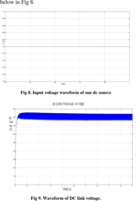
The proper integration of the sources is ensured by simulating the system in MATLAB/SIMULINK and the waveforms are validated. A three phase AC source of 440V, 50Hz and three separate DC source of 220V each are integrated to grid using NVSC.
Fig 6(a). SIMULINK model of the VMC.
The simulation block diagram of the entire system is shown in the Fig 6(a). and the NVSC subsystem is shown in Fig 6(b)
Fig 6(b). SIMULINK model of NVSC subsystem.
V.SIMULATION RESULTS
The waveform of input ac voltage is shown in Fig.7
[image:3.595.54.270.145.350.2] [image:3.595.322.542.336.503.2] [image:3.595.318.553.517.696.2]International Journal of Emerging Technology and Advanced Engineering
Website: www.ijetae.com (ISSN 2250-2459,ISO 9001:2008 Certified Journal, Volume 4, Issue 2, February 2014)
[image:4.595.48.289.149.503.2]The input voltage waveform of one dc source is shown below in Fig 8.
Fig 8. Input voltage waveform of one dc source
Fig 9. Waveform of DC link voltage.
The waveform of dc link voltage from the NVSC is shown in the Fig 9. And the waveform of output voltage which is to be connected to the grid is shown in Fig 10.
VI.CONCLUSION
This paper proposed a versatile matrix converter for integration of ac/dc energy resources to the grid. The proposed converter operating in the reverse boost mode consists of nine switches for connecting a three phase ac source and three dc sources to the grid. It is applicable to all new alternative resources. With the proposed modulation and control schemes, nearly sinusoidal input and output current waveforms and proper power dispatches are ensured. The simulation results also confirm the same.
REFERENCES
[1] Xiong Liu,Poh Chiang Loh, Peng Wang, and Frede Blaabjerg, ―A Direct Power Conversion Topology for Grid Integration of Hybrid AC/DC Energy Resources‖, IEEE transactions on industrial electronics, vol. 60, no. 12, december 2013.
[2] X. Liu, P. Wang, and P. C. Loh, ―A hybrid AC/DC micro-grid and its coordination control,‖ IEEE Trans. Smart Grid, vol. 2, no. 2, pp. 278–286, Jun. 2011.
[3] S. Jain and V. Agarwal, ―An integrated hybrid power supply for distributed generation applications fed by nonconventional energy sources,‖ IEEE Trans. Energy Convers., vol. 23, no. 2, pp. 622– 631, Jun. 2008.
[4] W. Jiang and B. Fahimi, ―Multiport power electronic interface— Concept, modeling, and design,‖ IEEE Trans. Power Electron., vol. 26, no. 7, pp. 1890–1900, Jul. 2011.
[5] H. Hojabri, H. Mokhtari, and L. Chang, ―A generalized technique of modeling, analysis, and control of a matrix converter using SVD,‖ IEEE Trans. Ind. Electron., vol. 58, no. 3, pp. 949–959, Mar. 2011.
[6] T. Friedli, J. W. Kolar, J. Rodriguez, and P. Wheeler, ―Comparative evaluation of three-phase AC–AC matrix converter and voltage DC-link back-to-back converter systems,‖ IEEE Trans. Ind. Electron., vol. 59, no. 12, pp. 4487–4510, Dec. 2012. [7] L. Helle, K. B. Larsen, A. H. Jorgensen, S. Munk-Nielsen, and F.
Blaabjerg, ―Evaluation of modulation schemes for three-phase to three phase matrix converters,‖ IEEE Trans. Ind. Electron., vol. 51, no. 1, pp. 158–171, Feb. 2004.
[image:4.595.48.283.546.711.2]International Journal of Emerging Technology and Advanced Engineering
Website: www.ijetae.com (ISSN 2250-2459,ISO 9001:2008 Certified Journal, Volume 4, Issue 2, February 2014)
329 AUTHOR’S BIOGRAPHY
V. Kandasamy received B.E degree in Electrical and Electronics Engineering from Bharathiar University, Coimbatore, India in 1998, the M.E degree in VLSI Design from SASTRA University, Thanjavur, India in 2003, pursuing Ph.D. degree from Anna University, India. He is currently working as an Associate Professor at Kumaraguru College of Technology, Coimbatore, India. His current research Wind Energy Power Converters, FPGA based system Design.
R. Manoj completed his B.E. in Electrical and Electronics Engineering in SNS College of Technology, Coimbatore and currently pursuing his M.E in Power Electronics and Drives in Kumaraguru College of Technology,Coimbatore.