LOW POWER ASYNCHRONOUS FPGA ARCHITECTURE FOR
EFFICIENT DATA TRANSFER
Sathyendran and V. J. K. Kishore Sonti
Department of Electronics and Communication Engineering, Sathyabama University, Chennai, Tamil Nadu, India E-Mail: [email protected]
ABSTRACT
In recent years, Field Programmable Gate Arrays are used as reconfigurable architecture in various platforms as a special type processor which allows the end user to configure directly. The Logic Blocks and switch matrix provides an extensive use in the reconfigurable computing, that can be configured according to required application which also consumes lots of standby power with reduced throughput. This project investigates in optimizations of reconfigurable FPGA cells that involves in two stages, optimization of Lookup Table (LUT) in Logic Blocks for Large Application and optimization of switch matrix with encoding techniques. The proposed encoding technique combines four-phase dual-rail encoding and LEDR (Level-Encoded Dual-Rail) encoding; Lookup Table consists of 8 inputs which are extensively used for large applications; sleep controller design is used for reducing the standby power consumed by the LUT. The proposed architecture is designed, evaluated and simulated using Xilinx SPARTAN 3E (X3SC50).
Keywords: Field Programmable Gate Array (FPGA), Level Encoded Dual Rail (LEDR) Encoding, Logic Block, Lookup Table, Sleep Controller.
1. INTRODUCTION
Field-Programmable Gate Arrays (FPGAs) are widely used to implement special-purpose processors. FPGAs are cost-effective for small-lot production because functions and interconnections of logic resources can be directly programmed by end users. In commercial FPGAs, the clock distribution power is a serious problem because it has an enormously larger number of registers than custom VLSIs. To solve the problems caused by the clock, asynchronous FPGAs are proposed. Instead of using the clock, the asynchronous FPGAs use the handshake protocol between their components in order to perform the necessary synchronization and communication. Therefore, asynchronous FPGAs are low power because of no dynamic power in inactive circuits. The major disadvantage of FPGAs is its low performance because of the following reasons.
The area and delay of a switch block become
large since a switch block consists of many programmable switches.
The time for data transfer between logic blocks
becomes large since data from one logic block usually traverse through many switch blocks to reach the other logic block.
This paper presents a low power FPGA that uses an LUT-level power gating technique called autonomous
fine-grain power gating. To reduce the dynamic power consumption, we introduce Level Encoded Dual Rail (LEDR) based architecture. Time Multiplexed Level Encoded Dual Rail based architecture is yet another encoding technique proposed, in the view of reducing the area as well as the propagation delay of the entire circuit. The sleep controller used to reduce the standby power that is being consumed by the Lookup Table. The overall circuit occupies lesser area than the currently existing methods; hence these methods are integrated to reduce the power consumption of our FPGA.
2. RELATEDWORK
A. Asynchronous FPGA
Figure. 1. Dual Rail Encoded for N Bits
B. Four Phase Dual Rail Encoding
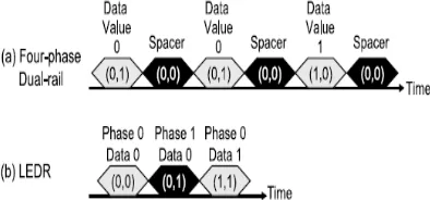
Reference [5] Four-phase dual-rail encoding is the type of dual rail encoding mostly used by asynchronous FPGAs, because of relatively small hardware cost. Figure 2(a) shows an example where data values 0, 0 and 1 are transferred. The sender sends spacer (0, 0) after a data value. The receiver knows the arrival of a data value by detecting the change of either bit: 0 to 1. The drawback of the four phase dual-rail encoding is low throughput because of the insertion of spacers.
C. Level Encoded Dual Rail Encoding
In LEDR encoding, no spacer is required. It enhances the throughput of the delay insensitive encoding. Figure 4 shows the example where data values “0” “0” and “1” are transferred. The sender sends data values alternately in phase 0 and phase 1 [8]. The receiver knows the arrival of a data value by detecting the change of phase. The drawback of the LEDR encoding is that it requires slightly complex hardware.
Figure 2. (a) 4 Phase Dual rail Encoding and (b) LEDR Encoding
D. Power Gating Technique
Overcome the problems of coarse grain power gating we introduce the Fine grain power gating technique. In fine grain power gating technique each look up table having own sleep controller and related to sleep transistor, so any of the lookup table active states all other lookup table are goes to sleep state. In this
[image:2.612.344.524.157.213.2]paper reduce the both standby power and dynamic power [3].
Figure 3. Control Strategy of the Proposed Power Gating
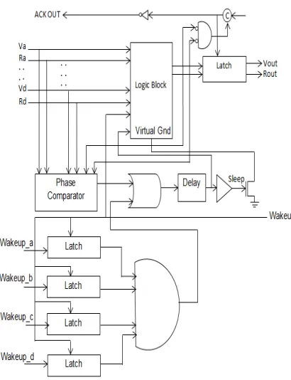
The proposed autonomous fine grain power gating is shown Figure 2. This is an efficient control strategy of the autonomous fine-grain power gating. The standby state is used to do the following:
Wake up the LB before the data arrives
Power OFF the LB only when the data does
not come for quite a while.
The use of the standby state has two major advantages. First, the wake-up time can be hidden since the LB has already been woken up when the data arrivals. Second, the dynamic power can be saved since the number of the unnecessary switching of the sleep transistor is reduced
[image:2.612.97.294.463.555.2]3. ARCHITECTURE DESIGN
[image:3.612.74.299.107.270.2]
Figure 4. Proposed Architecture
[image:3.612.324.560.268.389.2]The proposed Logic Block consist of the lookup table, sleep controller, registers and programmable delay elements presented. The description of the logic block described below[1].
Figure 5. Proposed CLB
A. Lookup Table Design
The Lookup Table architecture consists of three sub modules. Each sub modules consist of a decoder, a
multiplexer and memory register [1]. The decoder designed by two eight input AND gates. The output of the decoder is given to the multiplexer. The decoders exclude invalid input patterns for each phase. The data's which are valid are fed to the multiplexer. As a result, the transistor count is reduced compared to the multiplexer type LOOKUP TABLE which leads to reduction of the multiplexer. If the input combination are invalid (i.e., if the two inputs have the different phases) all pass transistors turn OFF according to the output of the decoder. The proposed lookup table showed in Figure 5.
Figure 6. Proposed Lookup Table
B. Sleep Controller
It contains phase comparator, latch and programmable delay design. It is discussed below Figure 7. The sleep controller design designed reference. The each block in the sleep controller described in below designs.
a) Phase Comparator Design:
The block diagram of a phase comparator for a four-input and one-output LOGIC BLOCK. The phase comparator is used to detect the data arrival. Phases of each data are extracted by XOR gates. If PHASE-A , PHASE-B, PHASE-C , and PHASE-D are different from PHASEOUT, then LOGIC BLOCK is active, and the output is ' 1' which means the new data has arrived to the logic block. Otherwise, it means that some data has not yet arrived and that the LOGIC BLOCK is not active and the output is '0'.The phase comparator output and pervious logic block wakeup signal given to the programmable delay.
b) Latch Design:
[image:3.612.96.301.365.632.2]
and no data arrives at the previous Logic Blocks, the output of the latch is reset to '0'.
c) Programmable Delay Design:
The function of the programmable delay is to delay the sleep signal by the predetermined threshold time. The programmable delay consists of a series of OR gates and several memory bits. The memory bits are used to program the delay time.
4. RESULTS AND DISCUSSION
A. Simulation Outcome
[image:4.612.305.544.109.207.2]The simulation results in Figure 7 shows that the proposed logic block is in active state when the data arrives. If the data arrives also the comparator output state is changing from “0” to “1” which the active process behind the data arrival. This has been repeated for various combinations of data and the simulated result coincides with the results. The signal of the sleep controller when it's high the next logic block goes to active state. The signal of the sleep controller when its low the next logic block goes to standby state till the next data arrives to the logic block.
Figure 7. Simulation Results of Proposed Architecture
B. Power Analysis
[image:4.612.314.550.318.438.2] [image:4.612.88.306.399.541.2]The power required to implement the Logic block after incorporating the developed fine-grain power gating LUT using the target device has been executed and tabulated below in Table I.
Table I. Power Report
C. Area Analysis
The total Logic utilization is shown in Table II. The number of LUTs was found to be same, number of Input Output Blocks (IOBs) was reduced in the proposed architecture and delay was increased.
Table II. Area and Time Analysis
LOGIC UTILIZATION
CONVENTIONAL LOGIC BLOCK
PROPOSED LOGIC BLOCK
Number of bonded IOBs
10 41
Delay(ns) 4.910 3.987
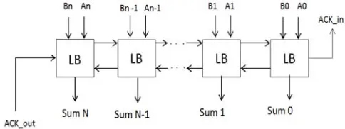
D. Implementation of Ripple Carry Adder
The ripple Carry Adder is implemented using proposed Logic Block is shown in Fig. 11. The Function unit acts as a Full Adder. The LUT produces the sum output and the carry logic produces the carry output.
Figure 8. Implementation of RCA
The comparison result for power analysis for implementation of Ripple Carry Adder is shown in Table III.
POWER SUMMARY
CONVENTIONAL LOGIC BLOCK
PROPOSED LOGIC BLOCK
[image:4.612.322.564.518.609.2]
Table III. POWER ANALYSIS FOR RIPPLE CARRY
ADDER
5. CONCLUSION
This paper proposes an asynchronous FPGA that combines four-phase dual-rail encoding and LEDR encoding with sleep controller to achieve small area, high throughput and low power and reduced standby power. The proposed architecture is also useful for large-scale.
REFERENCES
[1] Sathyendran. V and V.J.K Kishor Sonti. 2015.
Hybrid Reconfigurable Architecture with Autonomous Power Gating. International Journal of Computer Science and Engineering Technology (IJCSET). 6(02): 42-47.
[2] J. Teifel and R. Manohar. 2004. An Asynchronous
dataflow FPGA Architecture. IEEE Transactions on Computers. 53(11): 1376-1392.
[3] Masanori Hariyama. 2011. A Low Power FPGA
Based on Fine Grain Power Gating Shota Ishihara, Student Member. IEEE Trans. (VLSI) Systems. 1 9(8).
[4] M. Hariyama, S. Ishihara and M. Kameyama. 2008.
A low-power field-programmable VLSI based on a fine-grained power gating scheme. In Proc. IEEE Int. Midw. Symp. Circuits Syst. (MWSCAS), Knoxville. pp. 430-433.
[5] M. Hariyama, S. Ishihara, C.c. Wei and M.
Kameyama. 2007. A field programmable VLSI based on an asynchronous bitserial architecture. In Proc. IEEE Asian Solid-State Circuits Conf. (A- SSCC), Jeju, Korea. pp. 380-383.
[6] Zhengfan Xia, Shota Ishihara, Masanori Hariyama
and Michitaka Kameyama. An Asynchronous FPGA Based on Dual/Single-Rail Hybrid Architecture. Int'l Conf. Reconfigurable Systems and Algorithms, ERSA'12.
[7] Xilinx Inc., San Jose CA. 2009. Spartan-3 FPGA
family datasheet. [Online]. Available:
http://www.xilinx.com.
POWER SUMMARY
CONVENTIONAL LOGIC BLOCK
PROPOSED LOGIC BLOCK