http://dx.doi.org/10.4236/cs.2014.511029
A Novel Signal Processing Coprocessor for
n-Dimensional Geometric Algebra
Applications
Biswajit Mishra
1, Mittu Kochery
2, Peter Wilson
3, Reuben Wilcock
31VLSI & Embedded Research Lab, Dhirubhai Ambani Institute of Information and Communication Technology
(DAIICT), Gandhinagar, India
2Advanced RISC Machines Ltd. (ARM), Cambridge, UK
3School of Electronics and Computer Science, University of Southampton, Southampton, UK
Email: [email protected], [email protected], [email protected], [email protected]
Received 26 August 2014; revised 25 September 2014; accepted 8 October 2014
Copyright © 2014 by authors and Scientific Research Publishing Inc.
This work is licensed under the Creative Commons Attribution International License (CC BY). http://creativecommons.org/licenses/by/4.0/
Abstract
This paper provides an implementation of a novel signal processing co-processor using a Geome- tric Algebra technique tailored for fast and complex geometric calculations in multiple dimensions. This is the first hardware implementation of Geometric Algebra to specifically address the issue of scalability to multiple (1 - 8) dimensions. This paper presents a detailed description of the imple- mentation, with a particular focus on the techniques of optimization used to improve performance. Results are presented which demonstrate at least 3x performance improvements compared to previously published work.
Keywords
Geometric Algebra, Clifford Algebra, FPGA, GA Co-Processor
1. Introduction
source intensive applications such as computer graphics has been the efficiency with which solutions can be ob- tained. There has therefore been a strong interest in the area of developing high performance hardware engines that can accelerate the computations in the GA framework including [8] [9]-[16]. Unfortunately all these im- plementations are dimensionally specific rather than taking a general purpose and scalable n-dimensional ap- proach. There has recently been increasing interest in reconfigurable GA systems which are essential in a general- purpose GA engine to allow for multiple dimensions and different types of object to be analyzed [2]-[7] [9] [12]-[16]. As a result, there has been a strong motivation to extend the fixed architectures previously published and develop a modular n-dimensional GA co-processor on either an FPGA or ASIC platform.
In this paper, we present an alternative design of a Geometric Algebra co-processor and its implementation on a Field Programmable Gate Array (FPGA). To the best of the authors knowledge only four GA designs in hard- ware exist in the literature [8] [10] [14] [16] and the proposed design is the first implementation of a modular n- dimensional optimized GA architecture in hardware.
This paper is organized as follows. In Section 2, the fundamental concepts in GA are discussed. In Section 3 the top level GA co-processor architecture is introduced with an extended discussion in Section 4 for the GA coprocessor design. The key building blocks for the GA co-processor in blade logic, register file, and the mem- ory write sequencer are discussed in this section. The simulation, synthesis results and comparison to the state of the art are discussed in Section 5. Finally in Section 6, we conclude our findings.
2. Geometric Algebra
2.1. Basics Relations
Geometric Algebra (GA) is a coordinate-free approach to geometry based on the algebras of Grassman [17] and Clifford [18]. It introduces the concept of 2, 3 and higher dimensional subspaces, similar to the concept of vectors or 1-dimensional subspaces. It is possible to add, subtract, multiply and divide subspaces of different dimensions, result- ing in powerful expressions that can express any geometric relations as described in [7] and [17]-[21].
2.2. Blades
The concept of a blade is fundamental to all objects defined within a GA framework. Let the orthonormal basis vectors be e e1, 2 in 2-D GA and these can be decomposed into a linear space spanned by the following ele- ments:1, ,e e e1 2, 1∧e2. The individual element of this linear subspace is called a blade. Furthermore, the grade of the blade refers to the dimension for the space the blade spans.
The blade signifies the subspace i.e. scalar, vector or bivector. Hence the linear subspace consists of a scalar (1) a 0 blade element, vectors
(
e e1, 2)
which are 1 blade elements, a bivector(
e1∧e2)
is a 2 blade element, which has 0, 1 and 2 grades and represents 0, 1 and 2 dimensional subspaces respectively. The total number of basis blades for a n space with k blades is given by∑
( )
n k, =2n. These elements of then
Cl linear sub- space are called homogeneous elements and are given in Table 1.
2.3. Bivector and Trivector
In GA, the outer product is also known as the wedge product denoted by a∧b in a 2-dimensional subspace, an oriented area called a bivector. If b were extended along a the result would be another bivector with the same area but opposite orientation as shown in Figure 1.
The outer product works in all dimensions. If a 2-dimensional subspace a∧b is extended along another dimensional subspace c the resultant a∧ ∧b c is a 3-dimensional subspace or the trivector (shown in Fig- ure 2) and a directed volume element. In a 3-dimensional Euclidian space R3, there is one basis trivector
1 2 3 123 e ∧ ∧ =e e e .
2.4. Geometric Product and Multivector
Table 1.Elements of Cln geometric algebra.
n
Cl Basis blade Total
0
Cl 1 1
1
Cl 1,e 1 2
2
Cl 1, , ,e e e 1 2 12 4
3
Cl 1, , , ,e e e e e1 2 3 12, 23,e e 13,123 8
a
b
[image:3.595.142.486.83.408.2]a
b
a b
b a
∧
∧
[image:3.595.89.537.116.592.2]Figure 1.Bivector orientations.
Figure 2. Graphical representations of a trivector.
ab= ⋅ + ∧a b a b (1)
For the orthonormal basis vectors defined by ei and ej for the Rn space the rule as given in Equation (2) encapsulates the full algebra.
if
1 if
j i i j
e e i j
e e
i j
− ≠
=
=
(2)
For e1 and e2 the following holds good:
1 2 1 1 2 2
1 2 2 1 1 1 2 2
0, 1, 1
, 0, 0
e e e e e e
e e e e e e e e
⋅ = ⋅ = ⋅ =
∧ = − ∧ ∧ = ∧ = (3)
Generalizing, the geometric product of basis vectors ei and ej is:
( )
2( )
( )
1
i j i j i j i i j j i i j j
e e =e e e e = −e e e e = − e e e e = − (4)
The element ei∧ej is called the pseudoscalar which is the highest grade element and is denoted by a sym- bol i or I. The 2-D GA relationships for the orthonormal basis vectors are given inTable 2.
2.5. Hardware Implementation of GA
Table 2. Geometric algebra product within 2D.
1 e1 e2 e 12
1 1 e1 e2 e 12
1
e e1 1 e12 e 2
2
e e2 −e12 1 −e1
12
e e12 −e2 e1 −1
ALU to write evaluation results to the appropriate addresses of the on-board RAM on completion of an opera- tion.
Due to resource limitations on the hardware only a single basis blade pipeline was implemented for geometric products. The FPGA implementation ran at 20 MHz and in real terms, was found to be much slower than soft- ware packages like Gaigen [12] [23] running on typical PC platforms (such as a typical desktop 1.5 GHz ma- chine). The performance differences between software versions of GA and Linear Algebra in solving geometric problems is given in [12] and hardware versions of GA are discussed in [10] [11] [15] [16] [22]. In [10], the hardware was running at a slower clock rate than the software version of the algorithm, which was running on state of the art microprocessors, and therefore to compare the results they needed to be scaled and normalized first. In this normalized comparison, the hardware was found to be of comparable performance and about 1.5× faster than the software implementation of Gaigen on a CPU.
In [11], a GA that supports 4D GA operations is designed and implemented on an FPGA. The design consists of a CCU (Central Control Unit), RAM controller, RAM and ALU block with a PCI interface very similar to the design of [10]. It utilizes huge resources by taking up 24 16-bit multipliers and 16 32-bit adders. In [15] [16], the authors discuss the design and implementation of an embedded co-processor with support for 3D to 5D Clifford algebra. It also describes a multicore approach for GA operation support to be comparable to conventional ar- chitectures. The implementation takes advantage of embedded multiplier cores within the FPGA, 24 multipliers for 3D and 64 multipliers for 4D and 5D co-processor implementation. In [8] [24] [25], a modular Geometric Algebra Micro Architecture (GAMA) co-processor design is proposed. This math co-processor has standard in- structions that could be extendible and interfaced to a standard processor and implements partial instruction- level parallelism. It evaluates the Geometric product, Inner and Outer product and also simple addition, multip- lication and division of multivectors. The design uses two pipelined floating-point multipliers, three pipelined floating-point adders and a controller consisting of a main controller and a pipeline controller.
In the next section of this paper, we will present the proposed architecture that is scalable to n (up to a maxi- mum of 8) dimensions.
3.
GA Co-Processor Architecture
Before discussing the architecture some basic GA definitions need to be made. If a and b is considered to be the multivectors in the Cl2 space:
0 1 1 2 2 3 12
0 1 1 2 2 3 12
a a a e a e a e
b b b e b e b e
= + + +
= + + + (5)
The geometric product is given by:
(
) (
)
(
0 01 3 1 10 2 2 22 0 3 33 1)
20 1(
0 31 0 1 22 3 2 13 2 3 01)
1 2ab a b a b a b a b a b a b a b a b e
a b a b a b a b e a b a b a b a b e e
= + + − + + − +
+ + + − + + − + (6)
Then if all the coefficients of a and b are non-zero, the simplest implementation for GA based computations for each multiplication between basis blades results in a separate multiplier hardwired to the appropriate multi- vector elements. Following the multiplication, an adder collects the output whose multiplications result in the same blade. In Cln, 22n
multipliers are needed and 1 0 2n n 2i
i
− =
3.1. Top Level Architecture
The top level module for the GA co-processor contains instances of GA Core, Memory, Memory Write Se- quencer and the Register File. In addition it contains the logic for the state machine that makes the GA co-pro- cessor function correctly and also contains the logic for converting between 40-bit and 16-bit data.
Figure 3 shows the internal structure of the GA module with various sub-modules and logic.
In the following subsections we discuss the register file, memory and memory sequencer and a detailed dis- cussion on the GA Coprocessor will be provided in the following section.
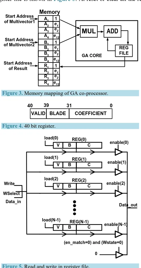
3.2. Register File
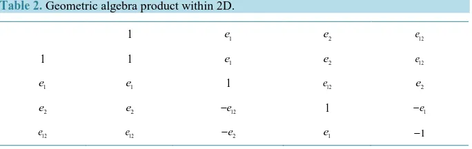
The register file is dual-ported with separate read and write selects. In case of the bypass mode, data can be di- rectly written from the sequencer or multiplier to the register file. Each register in the register file comprises of 41 bits. The structure of a single register is shown in Figure 4. The coefficient part of the multivector is fixed at 32 bits while the blade part is fixed at 8 bits (a maximum of 40 bits to accommodate 8D vector space).
The number of registers
(
3 2× n)
in the register file depends on the dimension of the vector space( )
n . The internal structure of the register file is shown in Figure 5. At reset or clear all the registers and counters in theMUL
ADD
REG FILE 1
e1 e2
e12
1
e1 e2
e12
1
e1 e2 e12
A1 A2 A3 A4 B1 B2 B3 B4 R1 R2 R3 R4 Start Address of Multivector1
Start Address of Multivector2
Start Address of Result
GA CORE
Memory
Figure 3.Memory mapping of GA co-processor.
VALID BLADE COEFFICIENT
40 39 31 0
Figure 4. 40 bit register.
V B C enable(N-1) REG(N-1)
load(N-1)
V B C enable(2) REG(2)
load(2)
V B C enable(1) REG(1)
load(1)
V B C enable(0) REG(0)
load(0)
(en_match=0) and (Wstate=0) Data_out Write
WSelect Data_in
[image:5.595.195.430.273.719.2]0
register file are cleared. The 41st bit of every register is the register valid bit (V) andit is set to “1” or “0” to in- dicate that the data it holds is valid or invalid respectively.
When the register file receives an active Write signal, WSelect is compared with bits 39 to 32 of every register which represents the blade information (B). If this matches for a register then its corresponding equal signal be- comes high. This is then used as the load signal to write to the register. If none of the registers match, then the data is written to the register pointed to by the counter. The counter is then incremented by one. Whenever data is written to a register, its valid bit is set to 1 indicating that the register holds valid data.
For reading from the register file, RSelect is again compared with bits 39 to 32 of every register. If this matches for a register, then its corresponding “en” signal becomes high. This is then used to enable that regis- ter’s tristate using the signal enable and the contents of that register are put on the Data_out bus. If none of the registers match, then zeroes are driven on the Data_out bus except in the memory write phase, when the bus is in a high impedance state.
3.3. Memory
The memory can be located inside or outside of the GA co-processor. In the proposed design the memory is lo- cated within the GA co-processor and each memory location is 40 bits wide which allows maximum data band- width to be obtained during processing.
The proposed memory model can be scaled using the generic parameter AddressWidth and the DataWidth that is set according to the dimension of the vector space. For example, in an 8D vector space at least 3 × 256 = 768 memory locations are required to store the two input multivectors and the resultant multivector and hence the address width is 10 bits.
3.4. Memory Write Sequencer
A Memory Write Sequencer is required to read data from the register file and write it to memory. After the processing phase the resultant multivector will be available in the register file. This is transferred to memory in the Memory Write phase.
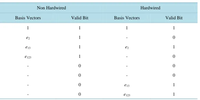
[image:6.595.143.487.550.722.2]In GA, often certain applications [9] [25] require a subset of multivector elements. For example, as shown in Table 3, if the elements present are 1, e2, e13, e123, it could be stored as contiguous blocks (non hardwired) or non contiguous blocks (hardwired). In the proposed design, zero registers occur as a single contiguous block while in the hardwired version, they occur in several blocks. The non-hardwired version avoids non-contiguous blocks of zero registers.
For example, in the hardwired version as shown in Table 3, 8 cycles are required to write its contents to memory in 3D GA that has 23 = 8 elements. On the other hand, to write the contents of the non-hardwired regis- ter file only 4 cycles are required. This is possible because the non-hardwired register file uses an extra bit, the 41st bit or register valid bit which can be checked by the Memory Write Sequencer. The savings in terms of clock cycles becomes noticeable while writing back the contents of the resultant registers to the memory and
Table 3. Hardwired and non-hardwired memory write sequencer.
Non Hardwired Hardwired
Basis Vectors Valid Bit Basis Vectors Valid Bit
1 1 1 1
e2 1 - 0
e13 1 e2 1
e123 1 - 0
- 0 - 0
- 0 - 0
- 0 e13 1
becomes more apparent for higher order vector processing. This will be discussed in detail in the experimental results section of this paper.
4. GA Core: Detailed Description
While the top level architecture of the basic n-dimensional GA co-processor has now been defined, in order to maximize the performance benefits it is essential to optimize each key element in the design. This section now describes each of the modules within the Geometric Algebra Co-processor in detail. Pipelining the multiplier and adder is crucial to achieve parallelization in the hardware.
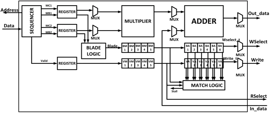
The proposed GA co-processor core (shown in Figure 6) contains the sequencer, multiplier and the adder. The core contains the registers which cause the Valid signal and the blade information to ripple through the pipeline. It also contains the logic for generating the Stall signal, the blade logic and the Process_End signal logic.
The signals MC1, MC2, MB1, MB2 and Valid are registered as CoeffA, CoeffB (C1 and C2), BladeA, BladeB and Valid respectively as shown in Figure 6. BladeA and BladeB travels through the blade logic. Depending on the value of Cfg_Bits, the signals Coeff, Blade and Valid goes either to the multiplier, adder or the register file.
4.1. Multiplier and Adder Pipelining
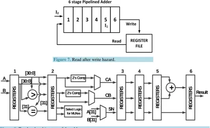
In the proposed design, the fixed point multiplier and adder are pipelined to improve the instruction throughput. Arbitrarily, the multiplier pipeline is 5 stages and the adder pipeline is 6 stages. However, the use of pipelined processing elements adds to the processing time and introduces the problem of data hazards.
Data hazards occur when the pipeline changes the order of read/write accesses to operands. For example, in the proposed design Read after Write (RAW) hazard can occur i.e. the register file is modified and read soon af- ter—the first instruction may not have finished writing to the register file, while the second instruction may use incorrect data.
Consider that two instructions I1 and I2 operate on the same blade as shown in Figure 7. In the next cycle of operation, I1 moves to stage 6 of the adder and I2 moves to Stage 1. But the operand read from the regis- ter file for instruction I2 is incorrect because it does not see the latest value which will only happen when I1 writes to the register file. This hazard can only be fixed by holding instruction I2 and stalling everything be- fore it until I1 writes to the register file. Therefore, to avoid data hazards, pipeline stalling is required which will be discussed in detail in the subsection describing stall (match) logic.
4.2. Multiplier
The design uses a standard fixed point signed 5-stage multiplier that takes two 32-bit input operands A and band returns a 32-bit product. The Most Significant Bit (MSB) in signed arithmetic indicates the sign.
REGISTER REGISTER BLADE LOGIC REGISTER MULTIPLIER BM 3 BM4 BM5
VM
1 VM2 VM3 VM4 VM5
ADDER
BA
2 BA3 BA4 BA5 BA6
VA
[image:7.595.94.536.522.711.2]2 VA3 VA4 VA5 VA6 BA 1 VA 1 MUX MUX MUX MUX MUX MUX MUX SEQUENCER Stall MATCH LOGIC BM 1 BM2 MC1 MB1 MC2 MB2 Blade Valid Address Data Out_data WSelect Write RSelect In_data Wselect_t Write_t
In normal operation, CoeffA and CoeffB become the inputs A and B of the multiplier respectively. Registered values of Blade and Valid enter the multiplier blade pipelines which are 5 stages. Together they form the multip- lier valid pipeline. Data in every stage of the multiplier has its blade and valid bit in the corresponding stage of the blade and valid pipeline. As shown in Figure 6, the 8-bit signals in the multiplier blade pipeline are called BM(1), BM(2), BM(3), BM(4) and BM(5). The signals in the valid pipeline are called VM(1), VM(2), VM(3), VM(4) and VM(5).
4.3. Adder
As shown in Figure 8, the 6 stage adder takes two 32-bit input operands A and B, and returns a 32-bit Result. The sign of the result is the sign of the operand with the larger magnitude. Depending on the magnitude and sign, the operands go directly or through a 2’s complement unit.
Similar to the multiplier, the 6-stage adder blade pipeline and a 6-stage adder valid pipeline exist for the adder. The 8-bit signals in the adder blade pipeline are called BA(1), BA(2), BA(3), BA(4), BA(5) and WSelect_t. The signals in the adder valid pipeline are called VA(1), VA(2), VA(3), VA(4), VA(5) and Write_t. As can be seen in Figure 6, BM(5) and VM(5) are fed directly to the adder blade pipeline and the adder valid pipeline respectively. In normal operation WSelect_t becomes WSelect and Write_t becomes Write. The result of addition goes to the register file through the bus Out_data.
4.4. Sequencer
The sequencer reads data from the memory and feeds it to the multiplier, adder or directly to the register file depending on the mode of operation. As shown in Figure 9, AD(xi) stands for the address of the data xi in mem-
ory. To mitigate the effects of wrong data the stall signal is used. It causes all the counters and registers to hold their value. A high on Stall means that the data from the sequencer has not been registered by the core, which could be the adder or multiplier or register file depending on the mode of operation.
That means the address which was sent to the memory just before the stall occurred has to be sent again for a fetch. Depending on when the stall occurs, different scenarios can occur. For example, in one scenario as shown in Figure 9, AD(b3) is put on the Address bus to be fetched. The data b3 is not registered in the following cycle as the stall signal is high. AD(b3) therefore has to be fetched and put on the Address bus again so that data b3 can be registered in the subsequent cycle.
REGISTER FILE
1 2 3 4 5 6
6 stage Pipelined Adder
Write
Read I2
I1
Figure 7.Read after write hazard.
REGISTERS REGISTERS REGISTERS REGISTERS REGISTERS REGISTERS [30:0]
[30:0]
[31] [31]
>
=
2's Comp
2's Comp
A
B
4 3
1 2
CA
CB
SN
+
Result6 5
Select Logic for MUXes A[31]
[image:8.595.107.525.460.714.2]B[31]
4.5. Blade Logic
The blade logic which explains the blade relationships within the algebra is central to the architecture and is discussed in the following.
4.5.1. Computation of Basis Blade Vector and Sign
The summary of blade index relationships has already been explained in Table 2. For example, to multiply with the resultant blade index is . Similarly if we multiply with then the resultant basis blade index is . This can be implemented by a multiplication table which is an approach followed by most soft- ware implementations. But the calculation of the blade part becomes more efficient when implemented in hardware.
Furthermore, the sign due to the blade index arises due to the invertible nature of the geometric operation. The sign is calculated from two evaluations, one arising from the swapping of the blade elements and the other due to the signature of the blades. For example, the sign due to swapping the blade index multiplication of with gives whereas with and results in . The resulting circuit is realized as a cascade of XOR and AND gates (Figure 10).
4.5.2. Signature Sign Logic
[image:9.595.180.450.336.708.2]The XOR gates account for the swapping of the blade elements and the AND gates for the blades. The signature for which the GA is defined also contributes to the sign element. For example in certain cases [13] in it is possible that some or none of the algebra elements square to and is implemented as shown in Figure 11.
Figure 9.Sequencer operation.
If the algebra is defined such that , then signature register is set as “1”. This contributes to the overall negative sign due to the XOR operation with the other outputs from the AND gates. The final sign com- putation due to swapping, signature and magnitude multiplication is obtained by XOR-ing the sign bits (Figure 11).
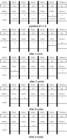
4.6. Stall Match Logic
The stalls in the architecture originate from the GA core and are required to avoid Read after Write (RAW) data hazards in the adder. The stall signals is the same as the match signal (as shown in Figure 12). There are 6 match signals for the 6 stages of the adder: match_d1, match_d2, match_d3, match_d4, match_d5 and match_d6. If any one of these goes high, then match goes high.
At reset, all the registers in the adder blade pipeline and adder valid pipeline are set to zero. This means that all data contained in the adder pipeline are invalid. The first valid data in the adder pipeline will be the first one with VM(5) set to high. If none of the blades in the adder pipeline match BM(5), then the signal match remains low. If the first valid blade is “00000000”, then it will match all the blade adder signals i.e. BA(1) to WSelect_t.
[image:10.595.233.391.307.410.2]Therefore, the match logic for each stage of the adder needs to be further qualified with its corresponding va- lid bits i.e. signals VA(1) to Write_t. That means only if there is valid data in BM(5) and a valid data in the adder with the same blade, the stall signal will be made high. The stall freezes the multiplier pipeline and the value of
Figure 11. Signature sign logic.
[image:10.595.200.431.425.710.2]Product, BM(5) and VM(5) will be held. When the stall is high, the GA core forces “00000000” into the adder blade pipeline and “0” into the adder valid pipeline. Therefore, the data which enters into the adder when the stall is high are all invalid. When the data which would have caused the hazard has been written to the register file, the stall signal goes low and allows the multiplier to push new data into the adder.
Figure 13 shows an example of pipeline stalls. Initially, the adder blade pipeline is assumed to have 6 distinct
BA(2) BA(3) BA(4) BA(5) WSelect_t
b2 b3 b4 b5 b6 b7 BA(1)
VA(1) VA(2) VA(2) VA(4) VA(5) Write_t
b3 BM(5) VM(5) 0 1 1 1 1 1 1 match
BA(2) BA(3) BA(4) BA(5) WSelect_t
b3 b4 b5 b6 b7 b0 BA(1)
VA(1) VA(2) VA(2) VA(4) VA(5) Write_t
b3 BM(5) VM(5) 1 1 1 1 0 1 1 match
BA(2) BA(3) BA(4) BA(5) WSelect_t
b4 b5 b6 b7 b0 b0 BA(1)
VA(1) VA(2) VA(2) VA(4) VA(5) Write_t
b3 BM(5) VM(5) 1 1 1 0 0 1 1 match
BA(2) BA(3) BA(4) BA(5) WSelect_t
b5 b6 b7 b0 b0 b3 BA(1)
VA(1) VA(2) VA(2) VA(4) VA(5) Write_t
b8 BM(5) VM(5) 1 1 0 0 1 1 1 match
BA(2) BA(3) BA(4) BA(5) WSelect_t
b1 b2 b3 b4 b5 b6 BA(1)
VA(1) VA(2) VA(2) VA(4) VA(5) Write_t
b7 BM(5) VM(5) 1 1 1 1 1 0 1
match match_d1 match_d2 match_d3 match_d4 match_d5 match_d6
pipeline at t = 0
after 1 cycle
after 2 cycles
after 3 cycles
after 4 cycles
blades b1 to b6. The adder valid pipeline indicates that the data in the adder corresponding to blade b2 is invalid. Also BM(5) contains blade of value b7 which is valid. Since b7 does not match any of the blades in the blade pipeline, the match signal remains low. In the next cycle, the data corresponding to blade b1 will be written to the register file. The rest of the data, blades and valid bits move forward through the pipeline. Now the value in BM(5) is b3 which is valid. As data of blade b3 is already being processed in the adder pipeline and it is in stage 5, the match_d5 signal goes high, which in turn generates a stall. The stall freezes all the pipelines before the adder and so the data, blade and valid bit will be held at the output of the multiplier. This can be seen in the fol- lowing cycle as the value of BM(5) and VM(5) remain the same.
Although the pipelines before the adder have frozen, the adder pipeline continues forward. A value of “00000000” which is represented by b0 is fed into the adder blade pipeline. The corresponding valid bit for this is set to zero indicating that this data is invalid and is used as a filler to fill up the pipeline. Now the data corres- ponding to b3 which was in Stage 5 is in stage 6, so match_d6 becomes high generating another stall. In the next cycle another invalid data of blade b0 is fed in so now b3 is written to the register file and match remains low. In the following cycle, the new data with blade b3 is fed into the adder pipeline. It uses the correct, updated value of b3 from the register file. So, in this example a two cycle stall is required to avoid the data hazard.
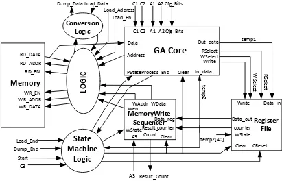
4.7. GA Co-Processor Operation
The block labeled “LOGIC” on Figure 14 multiplexes the addresses, data and memory enable signals on to read/write ports of the memory depending on the state of the state machine. This module contains the state ma- chine (shown in Figure 15) required for the GA coprocessor to function. At reset, the GA co-processor will be in the idle state. When the Start signal goes high, the state machine moves to the clearall state. In this state the signal Clear goes high that is used to clear all the counters and registers before starting an operation in the GA co-processor. In addition to the Clear signal, the signal CReset also becomes high. CReset is used to reset the counter in the Register File. This state is put initially because the GA co-processor can always hold the values from the last operation as it remains in the idle state. The clearall state is 1 cycle long and the state machine then moves into the load state.
During the load state, data is loaded into the memory. Once the coefficients of multivector 1 and 2 (C1 and C2) are loaded in memory (specified by A1 and A2), the Load_End signal goes high. This causes the state machine
Conversion
Logic
Write WSelectRSelect RSelect Write WSelect Out_data Data_in Data_out In_data temp1 temp 2 counter counter Data_regState
Machine
Logic
WAddr WData WenMemory
RD_DATA RD_EN RD_ADDR WR_DATA WR_ADDR WR_EN Data Address temp2[40] PStateProcess_End ClearC1 C2 A1 A2Cfg_Bits
WState Clear CReset Clear WState A3 Result_ Count Load_End Dump_End Start C3 Dump_Data Load_Data Load_Address Load_En
C1 C2 A1 A2 Cfg_Bits
[image:12.595.106.517.440.707.2]Result_Count A3
GA Core
MemoryWrite
Sequencer
Register
File
LOGIC
idle
memorydump Start=1 Dump_End=1
clearall
writeback
writesetup processing
load
Load_End=1
Process_End=1
[image:13.595.185.441.86.305.2]counter>C3 temp2(40)=1 or
Figure 15. State machine.
to move to the processing state. In the processing state, the GA co-processor operates (specified by Cfg_Bits) on the data loaded in memory. A high on Process_End signal indicates the end of processing and the state machine moves to the writesetup state. In the writesetup state, CReset is asserted thus clearing the counter in Register File. In writeback state that follows the writesetup state, the Memory Write Sequencer writes the resultant multivector to memory.
There are two ways by which the state machine can move to the next state from writeback state. One is by looking for a “0”, the 41st bit of a register that indicates that there is no more valid data in the Register File. The second way of moving to memory write setup state is to check if the counter in the Register File exceeds the value specified by C3, a register value that stores the number of elements of the vector space. The first condition reduces the effective cycles by writing only the non-zero coefficients to memory while the second condition saves cycles by fixing an upper limit on the number of registers to be written to memory by looking at the di- mension of the vector space in which the operation is performed. After the writeback state, the state machine moves to the memorydump state. In the memorydump state, the addresses on the Load_Addressare loaded and the Load_En signal is asserted.
The data read from the memory is driven on the Dump_Data bus after converting the 40-bit data into 16 bits. For converting the data from the 16-bit to the 40-bit, two 16-bit registers are required.
4.8. Process End Logic
The signal Process_End indicates the end of the processing phase. This signal informs the state machine in the GA module that the processing has been completed and the GA co-processor can move on to the next state. If the end_of_read signal is high and all the data in the pipeline is invalid, then we can be sure that the last valid data fed into the pipeline from the sequencer has been written to register file, and the processing is complete.
There are 12 levels of registers in the pipeline between the output of sequencer and the register file. So if the signals Valid, VM(1) to VM(5), VA(1) to VA(5), Write_t and end_of_read are zero, Process_End can go high. If the multiplier or the adder in the design is to be replaced with versions with different number of stages then the multiplier blade pipeline, the multiplier valid pipeline, the adder blade pipeline and the adder valid pipeline should also be changed to match the number of stages in their respective units. The Process_End logic should also be changed to reflect the change in the number of pipeline stages.
5. Experimental Testing and Results
5.1. Experimental Results
de-sign we implemented the dede-sign in VHDL and targeted it to a FPGA platform. The first experiment was exe- cuted to compare the processing cycles and overhead required for the geometric operations in different dimen- sions and results shown in Table 4. This table shows the ideal cycles required for the geometric product between two multivectors with coefficients of all blades non-zero, the number of cycles required for loading the multi- vectors into memory, the number of cycles required for processing the multivectors, the number of cycles re- quired to write the resultant multivector back to memory, the effective number of cycles and the extra cycles required for each dimension when compared to the ideal. The effective number of cycles is the sum of the load, processing and memory write cycles.
The extra cycles account for the stalls and also the cycles introduced by the sequencer. The number of cycles for the ideal case varies as 22n where n is the dimension of the vector space. To load n data elements into mem- ory, 3n + 1 cycles are required where +1 is for the one cycle overhead for the load operation. To write n data elements of the resultant multivector to memory, n + 2 cycles are required where +2 cycles overhead is required, one of which is used to reset the counter in the Register File. As can be seen from Table 4, the extra cycles do not increase proportionally as the dimension is increased. For the smaller dimensions, more extra cycles are seen because there are fewer basis blades in the smaller dimensions and as a result more stalls occur. In the higher dimensions, a large number of basis blades imply that there are fewer cases of data hazards occurring in the ad- der pipeline which means fewer stalls.
For example, let us consider the number of cycles in each case for 3D vector space (row 4 in Table 4). The number of elements in each multivector is 8 so for the geometric product, ideally only 8 × 8 = 64 cycles are re- quired. As discussed earlier, to load the two multivectors, 48 + 1 = 49 cycles are required and the number of cycles required for processing are 94. The memory write takes 8 + 2 = 10 cycles assuming that all 8 coefficients in the resultant multivector are non-zero. The effective cycles are therefore 49 + 94 + 10 = 153. When compared to the ideal, 153 − 64 = 89 extra cycles are required. Additional cycles are required for the resultant multivector data in the memory to be brought out on the 16-bit wide output bus. The sum of the effective cycles and the ad- ditional cycles required to output the result is called actual effective cycles. For example, in 3D vector space, an additional 3 × 8 = 24 cycles are required making the actual effective cycles to 153 + 24 = 177. The actual effec- tive cycles in each dimension are shown in Table 4.
The second experiment was performed to target the proposed design on an FPGA platform. To verify these results from simulations, a3D-GA co-processor was implemented on a Xilinx Virtex-II FPGA. The logic gene- rates the Clock, n Reset and Start signal. The Start signal is active low signal which means a “0” on Start would make the state machine move from idle to clearall. This is necessary because Start is mapped to the user push button switch on the FPGA which generates an active low signal. The state machine in the GA module is modi- fied as follows. The memory dump state is removed and a new state called complete is added. The signal Finish goes high when the state machine is in the complete state.
[image:14.595.86.541.563.722.2]The synthesis result for dimensions 1 to 3 shows the usage of dual-ported select RAM memories and for higher dimensions it uses block select RAM memories. Furthermore, the design in the 8th dimension cannot be supported on this FPGA. For dimensions 1 to 6, there exists a critical path from the stall logic in GA core to the sequencer and then to memory. It is also observed that the design frequency decreases when it is scaled from 1D
Table 4. Processing cycles for ga coprocessor.
Dimension Ideal Load Processing Memory Write Effective Extra Result Dump Actual Effective
1 4 13 26 4 43 39 6 49
2 16 25 46 6 77 61 12 89
3 64 49 94 10 153 89 24 177
4 256 97 292 18 407 151 48 455
5 1024 193 1076 34 1303 279 96 1399
6 4096 385 4180 66 4631 535 192 4823
7 16,384 769 16,532 130 17,431 1047 384 17,815
to 6D. This is because the address widths and counter widths get scaled and as a result morelogic is required. To compare the performance of our proposed core to the state of the art, the frequency of operation is chosen at the lower bound i.e. 65 MHz. Table 5 shows the comparison of recent works on GA Coprocessor architecture im- plemented on hardware (custom IC, FPGA) platforms. The proposed GA Coprocessor offers a cycle count of 177, 455 and 1399 for 3D, 4D and 5D respectively. In comparison to [10], where the hardware resources are the same i.e. one multiplier and one adder the performance improvement is significant.
When calculating the GA operations the GOPS (Equation (7)) is particularly important because the designer is then able to determine whether the timing constraint put by the clock cycles and GOPS provided by that partic- ular implementation is relevant.
1 1
GOPS
noofcycles clkperiod latency
= =
× (7)
[image:15.595.89.539.497.700.2]where no of cycles is the number of processing clock cycles (column 4, Table 4) to calculate the geometric product. Based on the definitions Table 5 gives a comparison for different dimensions, GA processor perfor- mance in MHz, clock cycles, and Geometric Operations per Second (GOPS). This also provides a comparison to the GA coprocessor in [10] [11] [14]-[16]. We can see the Geometric Operations per Second column provides a 3 - 4 times improvement over this architecture. Also the proposed architecture is comparable or has a lower GOPS when compared to [11] [14]-[16]. This can be explained as following. In these designs more hardware resources have been used. For example, in [11], 24 multipliers and 16 adders have been used for 4D GA imple- mentation. Similar is the case with [14] where 140 operators (74 DSP48Es) are used respectively. The 74 DSP48Es are basically multiply and add units. In [15][16], the GOPS for 3D, 4D and 5D are 892.8, 246 and 84.7 respectively is achieved by using embedded multiplier cores that speed up the GA operations. The embedd- ed core uses 24 multipliers in 3D and 64 multipliers in 4D and 5D implementations. As can be seen from Table 5, the GOPS metric is dependent on the frequency of operation and hardware resources. If more hardware re- sources are available, then clearly the cycle time and hence the frequency can be improved. However for a scal- able architecture these vendor specific solutions are not a preferred approach. Moreover, to be consistent across all the various implementations and platforms, the GOPS was normalized (6th Column in Table 5). The norma- lized GOPS (absolute values) is obtained by dividing the actual GOPS with the hardware resources used in that particular design. For example, for design in [10] the 112.52 GOPS is divided by 2, as the design has used one adder and one multiplier. (An otherwise normalization treating 1 multiplier and 1 adder as a single hardware re- source results in same conclusion). When the result is normalized for [15][16] with the hardware resources used, it can be seen that instead of the higher GOPs; 37.2 GOPS is obtained for 3D and 3.8 and 1.3 GOPS is obtained
Table 5. Comparison with the state of the art.
Reference Frequency (MHz) Resources HW Processing Cycles No of (In Thousands) GOPS (In Thousands, NormalizedGOPS ‡)
Perwass et al. [10] 20.0 1 M, 1A (2) 1761, 5442, 20443 112.521, 36.752, 9.793 56.26, 18.37, 4.89
Mishra & Wilson [24] 68.0 2 M, 3A (5) 841,2242,7043 809.61, 303.72, 96.623 161.92, 60.74, 19.32
Gentile et al. [11] 20.0 24 M, 16A (40) 562 357.15 8.9
Lange et al. [14] 170.0 74† 3663 464.5 6.28
Franchini et al.[15] 50 24 M 561 892.8 37.2
Franchini et al.[16] 100 64 M
4052 246.9 3.8
11803 84.7 1.3
This Work 65.0 1 M, 1A (2)
1771 367.2 183.6
4552 142.8 71.4
13993 46.4 23.2
1GA in 3D; 2GA in 4D; 3GA in 5D; M = Multiplier, A = Adder; †Number of DSP48Es in Xilinx (These are Multiply and Add Units); ‡Normalized to
for 4D and 5D respectively. As can be seen from Table 5, the proposed architecture has therefore the best GOPS compared to other implementations. Moreover, the proposed architecture achieves a smaller area, modular and is superior to the closest FPGA implementation by a factor of 3X to 5X in 3D to 5D implementations.
5.2.
Further Optimizations
In the current design the resultant multivector is first written from the register file to the memory and then later it is transferred to the output port from the memory. This is clearly not required as the result could be transferred from register file to the output memory directly. In that case the states writesetup and writeback can be removed from the state machine and the new state registerdump replaces memorydump. In the registerdump state the contents of the register file is put out on the output bus. As the output bus has a smaller bandwidth (i.e. 16 bits as compared to 41 bits in the register file), 3 times the clock cycles will be required. Then the actual effective cycles for the design can be obtained by subtracting the cycles for memory write phase and accounting for the cycles required for transferring the contents of the register file directly to the output bus. For example, in 3D the actual effective cycles could be 167 (177-10). Instruction-level parallelism exists when instructions in a se- quence are independent and thus can be executed in parallel by overlapping [26] to get performance improve- ment. Due to resource conflict this kind of parallelism is limited in this design. Only when the operation is in Result Dump phase, the memory is free and so the memory load or processing phase of the subsequent operation can be overlapped.
It was observed that for higher frequency of operation the timing critical paths should be broken. The timing critical path in the register file arising from the match logic can be broken at the cost of more resources in the register file. For example, in the 8th dimension, if there are another 2 set of comparators in the register file, then part of the match signal can be generated one stage earlier. This means that 4 × 256 = 1024 8-bit comparators are required in the register file. As the logic is split between two stages, the number of levels of logic between each stage can be reduced resulting in an increase of frequency.
For improving the effective number of cycles for operation, more than one GA Core, each with its multiplier, adder and independent register files can be used. In such a case, a common sequencer feeds data to the different cores. The complexity in this multiple GA Core design lies in the sequencer which should sequence data such that each pipeline works efficiently without many stalls. The sequencer has to intelligently feed data into the different GA Core pipelines to eliminate dependencies. This would also mean the use of buffering and additional memory.
Furthermore, the GA co-processor is envisaged to interface with a standard processor. This can be achieved in two ways, either by mapping the GA co-processor into the physical memory and giving it a real address on the address bus (memory mapped I/O) or by mapping it into a special area of input/output memory (isolated I/O) [27]. When it is mapped to memory, it can be accessed by writing or reading to the physical memory. Isolated I/O is isolated from the system and is accessed by ports using special machine instructions. Depending on the control signals, the processor reads or writes to the memory directly or to the GA co-processor through the iso- lated memory. In such a case, the GA co-processor requires a wrapper to interface with the standard core. This GA wrapper receives the operation instruction and control signals from the standard core that contains registers which need to be set up before any operation on the GA co-processor.
The VHDL code is provided for general download and use in the repository [28].
6. Conclusions
An alternative design of a Geometric Algebra co-processor was successfully created. The design was success- fully synthesized and functionally tested on an FPGA. We present a comparison of different FPGA and ASIC platforms in terms of performance and modularity of the architecture. On the FPGA, we developed a custom implementation for GA Geometric Product, which can be easily extended to other products within GA. We have introduced a modular architecture of the GA core linearly dependent on the dimension register file which can support up to an 8 dimensional GA can support up to an 8 dimensional GA, with a normalized performance that is better than previously reported results.
FPGA architecture was able to provide a flexible platform that could handle a variety of GA products without performance degradation, particularly being able to use multiple dimensions in a single implementation. Finally, the GA platform provides the opportunity to expand the GA instruction sets and also accommodate multiple cores, increasing the computational capacity, making an even more compelling GA platform for various applica- tions.
References
[1] Dorst, L. and Mann, S. (2002) Geometric Algebra: A Computational Framework for Geometrical Applications (I).
IEEE Computer Graphics and Applications, 22, 24-31. http://dx.doi.org/10.1109/MCG.2002.999785
[2] Mann, S. and Dorst, L. (2002) Geometric Algebra: A Computational Framework for Geometrical Applications (II).
IEEE Computer Graphics and Applications, 22, 58-67. http://dx.doi.org/10.1109/MCG.2002.1016699
[3] Lasenby, J., Gamage, S., Ringer, M. and Doran, C. (2001) Geometric Algebra: Application Studies. Geometric Alge- bra—New Foundations, New Insights.SIGGRAPH 2001, New Orleans.
[4] Lasenby, J., Gamage, S. and Ringer, M. (2000) Modelling Motion: Tracking, Analysis and Inverse Kinematics. AFPAC’00:
Proceedings of the 2nd International Workshop on Algebraic Frames for the Perception—Action Cycle. Springer-Ver- lag, London, 104-114.
[5] Lasenby, J., Fitzgerald, W.J., Lasenby, A.N. and Doran, C.J.L. (1998) New Geometric Methods for Computer Vision: An Application to Structure and Motion Estimation. International Journal of Computer Vision, 26, 191-213.
http://dx.doi.org/10.1023/A:1007901028047
[6] Lasenby, J. and Stevenson, A. (2000) Using Geometric Algebra for Optical Motion Capture. In: Bayro-Corrochano, E. and Sobcyzk, G., Eds., Applied Clifford Algebras in Computer Science and Engineering, Birkhauser, Boston, 147-169.
[7] Hestenes, D. (1986) New Foundations for Classical Mechanics. D. Reidel Publishing Company,Dordrecht, xi + 644 p. http://dx.doi.org/10.1007/978-94-009-4802-0
[8] Mishra, B. and Wilson, P. (2005) VLSI Implementation of a Geometric Algebra Micro Architecture. Proceeding of ICCA 2005. ICCA, Toulouse.
[9] Hildenbrand, D. (2005) Geometric Computing in Computer Graphics Using Conformal Geometric Algebra. Computers and Graphics, 29, 795-803. http://dx.doi.org/10.1016/j.cag.2005.08.028
[10] Perwass, C., Gebken, C. and Sommer, G. (2003) Implementation of a Clifford Algebra Co-Processor Design on a Field Programmable Gate Array. In: Ablamowicz, R., Ed., Clifford Algebras: Application to Mathematics, Physics, and En- gineering, ser. Progress in Mathematical Physics, 6th International Conference on Clifford Algebras and Applications, Cookeville, TN. Birkhäuser, Boston, 561-575.
[11] Gentile, A., Segreto, S., Sorbello, F., Vassallo, G., Vitabile, S. and Vullo, V. (2005) CliffoSor: A Parallel Embedded Architecture for Geometric Algebra and Computer Graphics. 7th International Workshop on Computer Architecture for Machine Perception, CAMP’05, Palermo, 4-6 July 2005, 90-95.
[12] Fontijne, D. and Dorst, L. (2003) Modeling 3D Euclidean Geometry. IEEE Computer Graphics and Applications, 23, 68-78. http://dx.doi.org/10.1109/MCG.2003.1185582
[13] Hildenbrand, D., Fontijne, D., Perwass, C. and Dorst, L. (2005) Geometric Algebra and Its Application to Computer Graphics. 25th Annual Conference of the European Association for Computer Graphics, Grenoble, 30 August-3 Sep- tember 2005.
[14] Lange, H., Stock, F., Koch, A. and Hildenbrand, D. (2009) Acceleration and Energy Efficiency of a Geometric Algebra Computation Using Reconfigurable Computers and GPUs. 17th IEEE Symposium on Field Programmable Custom Com- puting Machines, FCCM’09, Napa, 5-7 April 2009, 255-258.
[15] Franchini, S., Gentile, A., Sorbello, F., Vassallo, G. and Vitabile, S. (2009) An Embedded, FPGA-Based Computer Gra- phics Coprocessor with Native Geometric Algebra Support. Integration, the VLSI Journal, 42, 346-355.
http://dx.doi.org/10.1016/j.vlsi.2008.09.010
[16] Franchini, S., Gentile, A., Sorbello, F., Vassallo, G. and Vitabile, S. (2013) Design and Implementation of an Embed-ded Coprocessor with Native Support for 5D, Quadruple-Based Clifford Algebra. IEEE Transactions on Computers, 62, 2366-2381. http://dx.doi.org/10.1109/TC.2012.225
[17] Grassmann, H. (1877) Der ort der Hamilton’schen quaternionen in der aushdehnungslehre. Mathematische Annalen, 12, 375-386.
[18] Clifford, W.K. (1878) Applications of Grassmann’s Extensive Algebra. American Journal of Mathematics, 1, 350-358. http://dx.doi.org/10.2307/2369379
Dor-drecht.
[20] Hestenes, D., Li, H. and Rockwood, A. (2001) A Unified Algebraic framework for Classical Geometry. In: Sommer, G., Ed., Geometric Computing with Clifford Algebras, Springer, Berlin.
[21] Li, H., Hestenes, D. and Rockwood, A. (2001) Generalized Homogenous Coordinates for Computational Geometry. In: Sommer, G., Ed., Geometric Computing with Clifford Algebras, Springer, Berlin.
[22] Gebken, C. (2003) Diploma Thesis, Implementierung eines Koprozessors fur Geometrische Algebra auf einem FPGA. Master’s Thesis, Christian-Albrechts-University Kiel, Kiel.
[23] Fontijne, D. (2011) Gaigen Manual. http://www.sourceforge.net/projects/gaigen
[24] Mishra, B. and Wilson, P. (2005) Hardware Implementation of a Geometric Algebra Processor Core. Proceedings of ACA 2005. IMACS, International Conference on Advancement of Computer Algebra, Nara, 31 July-3 August 2005, 1-5.
[25] Mishra, B. and Wilson, P. (2006) Color Edge Detection Hardware Based on Geometric Algebra. 3rd European Confe-rence on Visual Media ProductionCVMP 2006, IET, London, 115-121.
[26] Stallings, W. (2003) Computer Organization and Architecture: Designing for Performance. 6th Edition, Pearson Edu-cation, Upper Saddle River.
[27] Buchanan, W. (1999) PC Interfacing, Communications and Windows Programming. Addison-Wesley, Boston.