http://dx.doi.org/10.4236/wjcmp.2016.62010
Metal-Semiconductor Interfaces
Investigated by Positron Annihilation
Spectroscopy
Abdulnasser S. Saleh
Department of Physics, University of Benghazi, Benghazi, Libya
Received 12 February 2016; accepted 2 May 2016; published 5 May 2016
Copyright © 2016 by author and Scientific Research Publishing Inc.
This work is licensed under the Creative Commons Attribution International License (CC BY). http://creativecommons.org/licenses/by/4.0/
Abstract
Variable-energy positron annihilation spectroscopy has been applied to study interfaces in Al/Si, Au/Si and Au/GaAs structures. Computational fittings of ROYPROF program were used to analyze Doppler broadening results in order to determine kinds of regions that positrons were likely to sample. The interfaces were found acting as a capturing thin layer with negligible positrons stopped in them and their characteristics came only from positrons diffusing to these interfaces, the positron work function of these materials were taken into consideration. In all fittings, the in-terfaces are found to have 1 nm thickness and act as an absorbing sink for all thermal positrons diffusing towards them, and this indicates either the existence of open volume defects or a weak-ness of known theoretical models for positron affinities. The result is supported by measurements obtained by applying external electric fields on Al/Si sample. Theoretical fittings have clearly demonstrated the sensitivity of interfaces in these attempts and their importance in data analyz-ing and in developanalyz-ing of fittanalyz-ing cods.
Keywords
Positron Annihilation, Interface, Metal-Semiconductor, Defects
1. Introduction
The importance of metal semiconductor interfaces comes from the fact that most electronic devices are inter-connected using metallic wiring that forms metal-semiconductor contacts. The properties of these contacts can vary considerably depending on the nature of the interface with the semiconductor.
in-terfacial regions of samples, and positrons of controllable energy are implanted into samples with mean energies between 0.1 and 25 keV, corresponding to mean depths from the surface to several micro meters.
When energetic positrons are implanted into a material, they rapidly undergo elastic and inelastic collisions with electrons. This process takes about 10 p sec. Phonon scattering then reduces the positron to thermal ener-gies. After some diffusion at these low velocities, the positron will annihilate with an energetic electron. The Doppler broadening of the two annihilation photons will therefore be mainly due to the motion of the lattice electrons. However, if positrons are trapped in point defects such as vacancies, the positrons will sample a dif-ferent distribution of electron velocities, and this may be seen in the reduced broadening of the 511 keV photon spectra recorded by germanium detector [1][2].
Analysis of annihilation gamma ray energy spectra yields information on atomic-scale structure via the mea-surement of Doppler broadening associated with the mean electron momentum at the annihilation sites, which is typically expressed by the single-number parameter S. The Doppler broadening S-parameter is defined as the counts in a central region of the annihilation peak divided by the total counts in the annihilation peak.
By analyzing the spectra, regions of the sample where positrons are annihilated can be easily determined but quantitative information and conclusions can be obtained only by fitting these results with a theoretical fitting [3].
There are many studies of different interfaces by positrons in literature and internal electric field associated with energy band bending is extensively studied [4]-[6], but the discussion on the need of First-principles calcu-lations rises more attention in the way that the interfaces are modeled [7]. Interfaces and heterostructures are considered complex systems and in order to understand measured positron annihilation parameters, a reliable computational modeling is required as the interaction of positrons with surfaces is not easy to model.
The motivation for these studies is how to treat interfaces when theoretical fittings of positron experimental results are required to obtain reliable information.
2. Positrons at Interfaces
To understand positron annihilation parameters measured for Metal-Semiconductor (MS) structure, the materi-al’s affinity and internal electric field in the depleted region must be accounted for. The simple physical form of the measured S parameter at certain energy E can be written as:
( )
epi epi( )
1 epi( )
s s( )
f f( )
i i( )
b b( )
S E =S F E + − F E S F E +S F E +S F E +S F E (1)
where Sepi, Ss, Sf, Si, Sb correspond to 100% annihilation in epithermal, surface, film, Interface and bulk
states and F(E)’s are respective fractions annihilating at each state. A computational fitting program with flexi-ble models is required to calculate these fractions, a vital need is the knowledge of materials positron affinities. The positron affinity A+ is a bulk property of materials. It is defined as a sum of electron (µ−) and positron
(µ+) chemical potentials,
A+=µ−+µ+. (2)
When two materials are in contact, the difference between their affinities determines the step of the positron potential at the interface [8]. In metals, when two materials are in contact, Fermi levels equilize themselves by charge transfer and the interface dipole D can be written as:
A B
D=µ− +µ− (3)
where µ−A and µ−B are electron chemical potentials for materials A and B while separated.
The difference between positron energy levels ∆E+ on sides of the interface E+A and E+B is given by:
AB A B A B
E+ E+ E+ D µ+ µ+
∆ = − = + − . (4)
Depending on the value of ∆E+, the potential well can be regarded as an attractive or repulsive for positrons.
When one of the materials is semiconductor, there are no extended charge states to accommodate the charge in the semiconductor side resulting in band bending [9].
3. Experimental Details
n-type GaAs substrates at room temperature and a base pressure of 10−5 Torr one at a time. The Si substrates were chemically cleaned by action and toluene, and finally HF dipped, then rapidly dried and loaded into the vacuum chamber and pumped down. The HF treatment is to remove the oxide layer usually exists on silicon wafers.
The samples were loaded at different times in the sample chamber of Herodotus positron beam at Royal Hol-loway University of London. Annihilation gamma energy spectra were recorded for incident positron energies E from 0.1 to 25 keV for half hour duration by a high-purity Ge detector system for each sample. Then the sample Aluminum on silicon structure was placed in the chamber with different external applied voltages (−10 V, +10 V and +45 V) and gamma spectra were recorded under each of these conditions. Finally, annihilation spectra were also recorded for the back of the Si and GaAS samples in order to obtain reference parameters for the two substrates.
4. Results
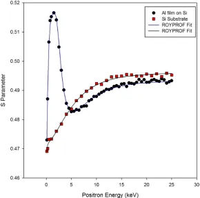
The S parameter was calculated for each spectrum at all positron energies by summing counts in 17 central channels divided by the sum of counts in 64 channels representing the whole annihilation peak. Figure 1 shows the calculated S parameter as a function of positron energy for the Al/Si (MS) structure sample, it also shows a curve of S parameter for bulk silicon (reference silicon), this is obtained from studying the back of the same sample. Two states are clearly seen, surface and bulk of the silicon. In the Al/Si MS structure curve, a clear peak at low energy represents the film followed by interface which is clearly seen at about 5 keV.
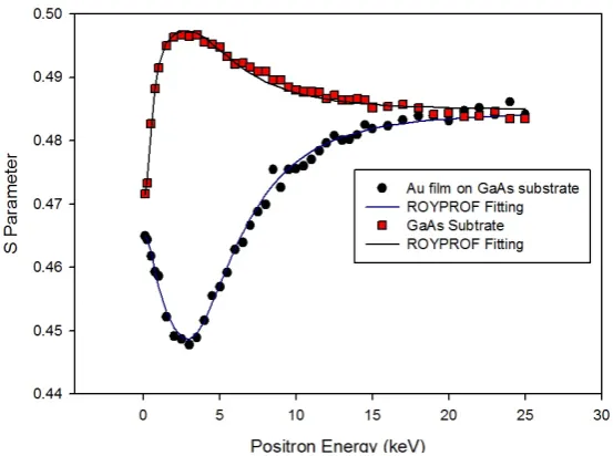
[image:3.595.166.457.393.680.2]In Figure 2, S parameters for the Au/Si sample are plotted against positron energies together with the curve of the bulk silicon, the Au film is seen as the lower part of the curve. The variation of S parameter with respect to the positron energy for Au/GaAs sample is shown in Figure 3, four regions are identified as, new surface, Au film (the lower part of S values), interface (at about 9 keV) and GaAs substrate, the top curve is the result of GaAs back side of the sample, two states as expected are seen with large existence of epithermal positrons signal.
Figure 1. Variation of S parameter as a function of positron energy (keV) in Al/Si sample and in Si substrate. The solid lines represent the best fits to the data using
Figure 2. Variation of S parameter as a function of positron energy (keV) in Au/Si sample and in Si substrate. The solid lines represent the best fits to the data
using ROYPROF.
Figure 3. Variation of S parameter as a function of positron energy (keV) in Au/GaAs sample and in GaAS substrate. The solid lines represent the best fits
to the data using ROYPROF.
5. Data Analysis and Discussion
[image:4.595.177.454.353.559.2]were tried by considering different interface thicknesses with all possible diffusion within, the best fitting is produced when thin interface (1 nm) thick with no diffusion is tried. Diffusion length of 60 nm is obtained for Al layer which indicates possible positron diffusion from the film to its surroundings. Values of 0.45785, 0.45824 and 0.49307 were obtained for Al film, interface and bulk silicon respectively, the S value of the inter-face is lower than S value for silicon bulk, this can only understood by the existence of oxygen at the interinter-face since trapped positrons tend to display higher S values than that for free positrons annihilating at the material bulk. Internal electric field strength of E = 5 × 10⁵ V/cm is also obtained from the fitting. It should be noted in Figure 1, the visible values at the bulk silicon do not match, that can be interpreted by the existence of high dif-fusion to the interface.
Similar fitting attempts were carried out for Au/Si sample data in Figure 2. The fitting has produced S values of 0.44826, 0.45172 and 0.49312 for Au film, interface and silicon substrate respectively, values of 96 nm and 76 nm are also obtained for film thickness and diffusion length in Au film. Internal field strength of E = 4 × 10⁵ V/cm is obtained. The interface location is not clearly visible in the S-E curve due to the fact that S values of the film and interface are close. Also best fit was obtained when the interface is considered absorbing sink for all thermal positrons diffusing towards it.
The fittings of curves in Figure 3 have produced values of 0.49786, 0.48145 and 290 nm for S value at the surface, S value at the bulk and diffusion length in reference bulk GaAs. Fitting of Au/GaAs data, the values of 0.44862, 0.49163 and 0.48131 were obtained for Au film, interface and GaAs bulk respectively, a film thickness and internal electric field of 74 nm and were E = 2 × 10⁵ V/cm were also obtained from the best fitting. Again after a large number of fitting attempts, the best fit was obtained for 1 nm thickness absorbing interface.
The film thicknesses 96 and 74 nm were obtained for Au films coated on Si and on GaAs. Although the coat-ing was done for the same time and under similar conditions, this difference can be related to the nature of sub-strates in terms of morphology, conductance and sticking coefficient.
Positron affinities of −6.24 eV and −7.90 eV were reported for silicon and GaAs [11], values of −4.28 eV and −6.1 eV for Aluminum and Gold [12]. In principle, and according to Equation (4) thermal positrons have the ability to diffuse in both directions at the interface.
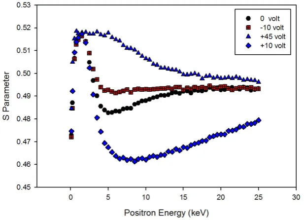
[image:5.595.160.469.456.679.2]The most important finding in this study is the full absorption of thermal positrons diffusing towards the in-terface. This theoretical finding is supported by experimental results obtained with external biasing on the Al/Si sample. These results are shown in Figure 4. A bias of −10 showed the majority of positrons annihilate at sili-con bulk and the characteristics of the interface are not seen, this means the majority of thermal positrons were
Figure 4. Variation of S parameter as a function of positron energy (keV) in Al/Si sample under external applied electric fields, a bias of +10 V in the direction of
drifted forward and the S value of the silicon substrate is seen just behind the S value of the film. On the other hand at +10 V where positrons were pushed back by the external field, the majority of positrons stopped at the substrate where thermally drifted to the interface and annihilate there, that is the reason behind the lowering of the curve to reach closer to the S value of the interface.
The curve obtained by applying +45 volts shows positrons were drifted backward to the Al film crossing the interface as the S value of the Al film is seen extending forward. The field produced by this relatively high bias cannot be maintained internally due to band bending, this result agrees well with idea of absorbing interface.
A study by Y. Y. Shan et al. [13] on Au/GaAs, has found similar curve as Figure 3, they have applied biases of 10 V and 25 V and the result agrees well with this study, they have concluded with the evidence of a perfectly capturing boundary.
The S values for different interfaces differ significantly among the three samples, this indicates the state of the interface is different for each structure as the S parameter reflects also the chemical composition.
Regardless of the nature of these interfaces in terms of nucleation and purity which cannot be investigated by positrons, this study supports the idea of considering absorbing interfaces in fitting positron data for film struc-tures produced by evaporation.
5. Conclusion
In conclusion, fitting study of positron annihilation data of different metal-semiconductor structures reveals the presence of positron absorbing interfaces, and they do not allow thermal positrons diffusing randomly or under influence of internal fields from crossing. This result is supported by other experimental data produced by applying external electric fields to one of the structures under study. The action of absorbing indicate ei-ther existence of open volume defects or a weakness in theoretical models of positron affinities. This achievement helps in fitting microstructure data and interface existing structures, and in developing computer codes.
References
[1] Schultz, P.J. and Lynn, K.G. (1988) Interaction of Positron Beams with Surfaces, Thin Films and Interfaces. Reviews
of Modern Physics, 60, 701-709.
[2] Tuomisto, F. and Makkonen, I. (2013) Defect Identification in Semiconductors with Positron Annihilation: Experiment
and Theory. Reviews of Modern Physics, 85, 1583-1631.
[3] Saleh, A.S. (2013) Analysis of Positron Profiling Data by ROYPROF, VEPFIT, and POSTRAP4 Codes: A
Compara-tive Study. Journal of Theoretical and Applied Physics, 7, 39.
[4] Ling, C.C., Shek, Y.F., Huang, A.P., Fung, S. and Beling, C.D. (1999) Electric-Field Distribution in Au-seminsulating
GaAs Contact Investigated by Positron-Lifetime Technique. Physical Review B, 59, 5751-5758.
[5] Brauer, G., Anwand, W., Skorupa, W., Revesz, A.G. and Kuriplach, A. (2002) Characterization of the SiO2/Si
Inter-face by Positron Annihilation Spectroscopy. Physical Review B, 66, Article ID: 195331.
[6] Maekawa, M., Kawasuso, A., Yoshikawa, M., Miyashita, A., Suzuki, R. and Ohdaira, T. (2006) Structure of SiO2/4H-SiC
Interface Probed by Positron Annihilation Spectroscopy. Physical Review B, 73, Article ID: 014111.
[7] Van de Walle, C.G., Lyons, J.L. and Janotti, A. (2010)Controlling the Conductivity of InN. Physica Status Solidi (a),
207, 1024-1036.
[8] Boev, O.V., Puska, M.J. and Nieminen, R.M. (1987) Electron and Positron Energy Levels in Solids. Physical Review
B, 36, 7786-7794.
[9] Puska, M.J., Lanki, P. and Nieminen, R.M. (1989) Positron Affinities for Elemental Metals. Journal of Physics:
Con-densed Matter, 1, No. 35. http://dx.doi.org/10.1088/0953-8984/1/35/008
[10] Saleh, A.S., Taylor, J.W. and Rice-Evans, P.C. (1999) The ROYPROF Program for Analyzing Positron Profiling Data
Obtained from Variable Energy Beams. Applied Surface Science, 149,87-96.
http://dx.doi.org/10.1016/S0169-4332(99)00179-8
[11] Panda, B.K. and Brauer, G. (1999) Positron Affinities and Deformation Potentials Are Calculated in Cubic Bulk
Sem-iconductor. Proceedings of the 30th Polish Seminar on Positron Annihilation, Jarnołtówek, 12-15 September 1998,
641.
Physics, 66, 841-897.
[13] Shan, Y.Y., Asoka-Kumar, P., Lynn, G.K., Fung, S. and Beling, C.D. (1996) Field Effect on Positron Diffusion in