Design and Comparative Analysis of Power
Efficient 14T Mux Based CMOS Adder Cell using
22nm Technology
Shakthi Rajashekar1 1
Department of Electrical and Electronics Engineering, Dayananda Sagar College of Engineering, Bangalore-78, India
Abstract: This Paper proposes a new mux based 14T adder cell designed to form a vital building block in computational systems. The performance metrics of the proposed full adder is compared by benchmarking with conventional and Shannon full adders. The designs also leverage the advantages of CMOS 22nm scaling when operated at a low power supply of 1v. Thorough simulations using HSPICE and PTM library models have been carried out on the adder cells considered and the parameters such as power, delay and PDP are investigated. The effect of temperature variation on the power consumption of proposed 14T mux based adder cell is also observed. The simulation results demonstrate that the proposed adder delivers stable output drivability with substantial diminution in the leakage power.
Keywords: Half adder, Full adder, adder cell, CMOS 22nm, low power, delay, PDP
I. INTRODUCTION
II. DESIGNOFHALFADDERS
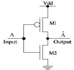
Initially performance of half adders with CMOS implementation has been analyzed. The conventional half adder requires 18 transistors to provide sum and carry outputs. Then the half adder design is improvised by a 6 transistor implementation [2] using transmission gates to reduce the area. Comparison of conventional method and transmission gate logic base technology has yielded the inference that in transmission gate based logic to implement adders, the complex expressions can be implemented by minimum number of transistors, fetching us the reduction in logic density. The NMOS transistor has the property of signal deprivation when supplied in chain of transistors with logic“1” while PMOS degrades for transmission of logic level “0”.In conventional half adder logic. If a transmission gate is employed in the design, perfect transmission can be obtained. The only problem with transmission gate are if several stages are incorporated then there is a chance of signal degradation and proper logic for on and off condition of transistors is important. The complemented bits for the inputs are obtained by implementing CMOS inverter at input stages and also for the carry logic. In Fig. 1 depicts the input to CMOS inverter i.e. if A is supplied with logic 0, the output Ā is pulled to Vdd by pull up (M1-PMOS device) during which the pull down (M2-NMOS device) will be shut off.[8] Similarly when the input A is supplied with logic 1, the output is pulled down to ground. The inputs are timed such that all combinations of half adder logic can be validated.
Figure 1. Conventional CMOS inverter
A. Boolean Expression For Half Adder
SUM = AB’+A’B (A XOR B) [3] CARRY = A.B (A AND B)
[image:3.612.240.369.270.392.2]The conventional CMOS circuit of half adder is depicted in figure 2. This logic implementation has 18 transistors including that of complemented inputs. Since the circuit is not found to be area efficient, A 12T transmission gate based half adder has been designed and analyzed
Figure 2. Conventional 18T half adder in CMOS logic.
[image:3.612.188.417.530.665.2]consumption. In the analysis, it has been observed that the transmission gate based half adder power consumption is reduced by 55.35 percent and also the transistor count is reduced by 33.33 percent in comparison with conventional half adder design.
Figure 3. 12T Half adder using Transmission gate
III. A.DESIGNOFFULLADDER
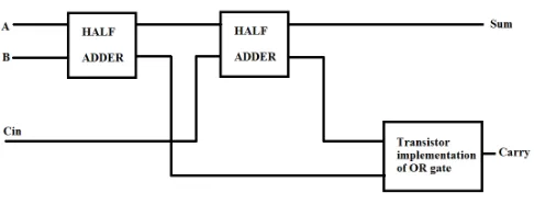
In the full adder design we incorporate an additional input carry-in along with the other two inputs of a half adder. In an n-stage addition, the carry-in (Cin) represents the output of a previous logic stage that has been fed as an input the current addition logic cell. The output of the full adder cell is designated as carry-out (Cout) that can be passed on to several stages and the Sum (S) is the resultant output of binary addition. The number of full-adders is proportional to the number of bits considered for addition. The full adder logic can be implemented by studying its truth table having all possible combination of input. The output S is an XOR operation between the input A and the half adder SUM output with B and Cin inputs. The carry out is found to be true only if any of the two inputs out of the three are high. Thus, we can implement a full adder circuit with the help of two half adder circuits. The first half adder is used to add A and B to produce a partial SUM. The second half adder is used to add Cin to the partial SUM produced by the first half adder to get the final SUM output. The carry of the half adders is ORed to get the final CARRY output. Figure 4 depicts the block diagram of a 1bit full adder.
Figure 4. Schmetic representation of full adder
Figure 5. Implementation of Full adder using Half adders
The expressions of SUM and Cout are
S = A’B’Cin + A’BCin’ + ABCin Cout = AB + ACin + BCin ---(1) Equaltion 2 represnts the boolean simplification of sum
S = A’B’Cin + A’BCin’ + ABCin = Cin (A’B’ + AB) + Cin’ (A’B + AB’)---(2)
Therefore S = Cin XOR (A XOR B) The carry expression is as follows
Cout = AB + ACin + BCin---(3) Cout = AB + ACin + BCin (A + A’)
=ABCin +AB + ACin +A’BCin = AB (1 + Cin) + ACin + A’BCin
= AB + ACin + A’BCin = ABCin + AB + A’BCin + A’BCin = AB (Cin +1) + AB’Cin + A’BCin
= AB + AB’Cin +A’BCin = AB + Cin (A’B + AB’)---(4) Therefore Cout = AB + Cin (A XOR B)---(5) Equaltion 5 represents the boolean simplification of carry
Based on the expresssions found in equations (2) and (5) the full adder circuit can be implemented using two half adders and an OR gate. The conventional full adder design has incurred 42 transistors including that of complemented inputs. In the design of full adder by cascading two half adders stages, we need 12 transistors for each half adder stage and an OR gate logic for carry output comprising of 6 transistos as depicted in figure. 6. The transcient analysis of this conventional full adder with 42 transistors at the normal temperature of 25 degree celcius has deliverd an average time delay of 5.021 ns for the input to output propagation. The maximum power consumption of the conventional 42T full adder is found out to be around 98.79 uW because of swift swithing of transistors for different input combinations.
The improved full adder using cascading of two half adders and an OR gate implementation provides reduced power consumpation. As the transistor count is reduced to 30 the dynamic swithcing has been be reduced leading to a drastic decline in power consumption to 30.21 uW. Also The simulation of this full adder at normal temperature at 25 degree celcius has incurred an average time delay of 7.02 ns. Also reduction in transistors leads to reduced parasitic capacitance and reduced output leakage current.
IV. B: IMPLEMENTATION OF OR GATE
transistion happens when only one of the NMOS devices turn on ( i,e. if either A or B is high ) for the NOR gate, The output is discharged when all inputs are driven high.
[image:6.612.209.412.141.246.2]Cascading the NOR output with CMOS inverter provides the OR logic suitable to offer the carryout signal computed from the cascaded half adders as described in (5)
Figure 6. Implementation of or gate using transistor.
V. SHANNON’SFULLADDER
A.SHANNON’S THEOREM
The Shannon theorem explains that the logic expressions are divided into two parts wherein in the first part a variable value is set to logic 1 and multiplied by a multiplier variable and in the next part the original variable that was set to logic 1 is then set to logic 0 followed by its multiplication with complement of multiplier variable. The entire logic can be reduced by repeating the Shannon’s theorem [1]The generalized Shannon expression of many variables is as depicted below.
F(a0 ,a1, a2,y ,ai, y, an) can be written as the sum of two terms, one with a particular variable (say ai) set to 0, and one with it set to 1. [1]
[image:6.612.187.443.517.711.2]f(a0,a1, a2….,ai,….,an) = ai’ f(a0, a1, a2……,0,….,an)+ ai f(a0,a1,a2,…1,…an).[1]
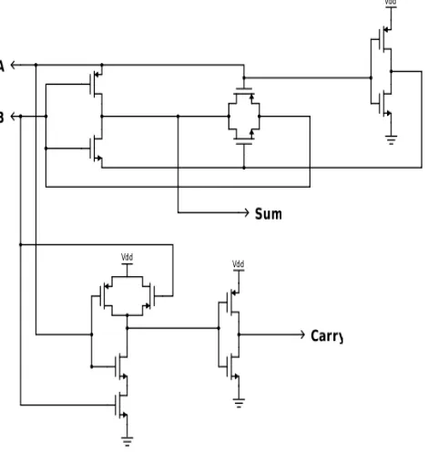
Fig 7 depicts the Shannon’s full adder network. In this (n-1) variables are used as control inputs connected to gates of the transistors based on whose value the data available at inputs of the pass transistors are transmitted towards the output[7]. In case of a one bit full adder in figure 7 the B and complement of B provide transmission path to original and complimented variables of A and Carr-in Thus realizing the sum expression in a modest transistor structure. Similarly the carry out is implemented by three control lines. In the represented structure it is important to note that control signal lines are connected to gates to control the switching and the data inputs are connected to drains of the transistors to pass the data. In carry out design we use carry in from a previous stage, Vdd logic1), and ground (logic0) as pass variables. In Shannon’s full adder, the sum logic is a two input XOR operation built with multiplexer method.
VI. 14TMUXBASEDCMOSADDERCELL
[image:7.612.192.411.242.412.2]The adder implementation using multiplexers has become fascinating topic in computational research in current shrinking technology due to the significance of targeted constraints such as area, power and speed. This paper proposes a one bit full adder by using 14 transistors targeted for low power consumption. The proposed design features conventional logic inversion wherever needed and avoided the Shannon based pass transition method for sum and carry. In the proposed circuit, by not using pass transistors it has been improvised reduce the effect of signal degradation that occurs due to passing of data in a longer adder chains. Since the design incorporates a low operating voltage of 1v, and a transistor count of 14 which yields lesser power consumption and parasitic capacitances[4]. Also the problem of voltage swing restoration can be avoided. The propagation speed from any of the three inputs to sum or carry outputs is also improved. The 14 transistor mux based adder is as fast as that of 30 transistors mux based full adder discussed earlier. his is achieved because of the implementation of three multiplexers implemented with two NMOS transistors is as depicted in figure 8 to select among input combinations of A,B and Cin. The maximum power consumption is significantly reduced to 1.656uW compared to all the designs discussed.
Figure 8. 14-T MUX CMOS adder circuit
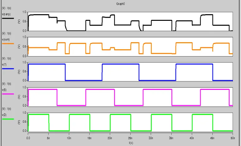
[image:7.612.113.500.483.718.2]The output waveform for design of the 14T MUX based full adder is as depicted in figure 9. The output validates the truth table of the conventional full adder. Figure 10 depicts the effect of temperature variation on the instantaneous power consumption of proposed 14T mux based adder cell.
Figure 10. Graph of Time versus Maximum power consumed at different temperatures
VII. COMAPARITIVE ANALYSIS
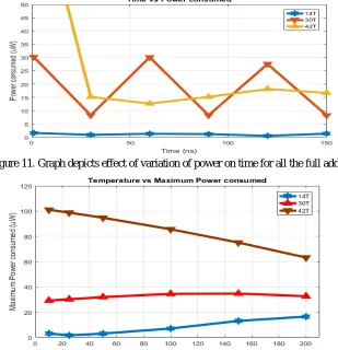
[image:8.612.150.459.384.704.2]In this section comparative analysis is carried out with respect to power and delay on the conventional 42T full adder, Transmission gate based 30T full adder and proposed 14T full adder. The below graph depicted in Figure 11 is time Vs power consumption. It infers that 14T mux based transistor has a significant reduction in power consumed
Figure 11. Graph depicts effect of variation of power on time for all the full adders
Figure 12 depicts the comparison of conventional and mux based full adders with respect to increase in operating temperature, it is observed that that the power consumed by 42T conventional full adder is high because of increased dynamic power consumption with increase in temperature. The transmission gate used 30T full adder has lower maximum power consumption but it fluctuates at equal time interval. The 14T low power MUX full adder has low power consumption throughout and a steady increase at high temperatures. This establishes that the 14T full adder has greater stability to heat occurred due to process variations or device switching overhead.
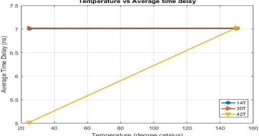
Figure 13. Graph depicts effect of variation of average time delay on temperature for all the full adders
Figure 13 depicts the effect of variation of temperature on propagation delay. It is observed that for mux based and transmission gate based adders, the delay is almost constant at 7 ns, whereas for conventional 42T full adder, there is a steady increase in delay with increase in temperature.
It is palpable that 14T mux based adder is having a stable speed of operation even under abnormal temperatures and it can be determined that the proposed adder can be incorporated high speed computation logic blocks.
VII. CONCLUSION
For low power operation and stable logic propagation this paper proposes a new 14T multiplexer based full adder designed with 22nm CMOS device scaling. The design has a maximum power supply of 1 volt and aspect ratio of 1:2 for pull up devices and 1:4 for pull down devices. The design has yielded the results that are rather less in power dissipation under linear variation of time and temperature. The adder also possesses a steady propagation delay when compared to conventional CMOS full adder, transmission gate based full adder and as well has Shannon’s full adder. With just 14 transistors in its architecture the leverage of this design is to incorporate the adder cell in multi bit high speed data computation systems.
REFERENCES
[1] S.Saravanan and M.Madheswaran, “Design of low power, high performance area efficient shannon based adder cell for neural network training” Control, Automation, Communication and Energy Conservation, 2009. INCACEC 2009. 2009 International Conference 4-6 June 2009, 978-1-4244-4789-3,” IEEE 2009.
[2] Ahmed M. Shams, Tarek K. Darwish, and Magdy A. Bayoumi, P erformance Analysis of Low-Power 1-Bit CMOS Full Adder Cells, IEEE Trans. on Very Large Scale Integration (VLSI) Systems, vol. 10, no. 1, pp. 20-29, Feb. 2002
[3] Dilli kumar, K. Charan kumar & T. Naveen kumar Design of high speed and low power six transistors full adder using twot ransistor XOR gat e IJECIERD,Vol. 3, Issue 1, Mar 2013
[4] Hassoune, D. Flandre, I. O'Connor and J. D. Legat,-ULPFA: A new efficient design of a power aware full adder, IEEE Transactions on Circuits and Systems I-5438, 2008
[5] A. P. Chandrakasan, S. Sheng, R. W. Bordersen, Low-power CMOS digit al design, IEEE JSSC, vol. 27, pp. 473-483, April 1992
[6] Uming Ko, PorasT. Balsara and Wai Lee, Low-Power Design Techniques for High-Performance CMOS Adders, IEEE Trans. on very Large Scale Integration (VLSI) Systems, vol. 3, no. 2, pp. 327-333,June 1995
[7] Radhakrishanan, S. R. Whit aker and G. K. Maki, Formal design procedures for pass-transistor swit ching circuit s, IEEE J. Solid-State Circuits, vol. 20, no. 3, pp. 531-536, June 1985
[8] Balaji Ramakrishna S, Dr. Aswatha A R- "Impact of Temperature Variation and Oxide Thickness Variation on the Performance of CNTFET Based Inverter in nanometer Regime" IEEE International Conference on Emerging Research in Electronics, Computer Science and Technology ICERECT-15 978-1- 4673-9563-2/15/ 2015
![Fig 7 depicts the Shannon’s full adder network. In this (n-1) variables are used as control inputs connected to gates of the transistors based on whose value the data available at inputs of the pass transistors are transmitted towards the output[7]](https://thumb-us.123doks.com/thumbv2/123dok_us/8294387.852345/6.612.187.443.517.711/depicts-shannon-variables-connected-transistors-available-transistors-transmitted.webp)