Synthesis of VHDL Code for FPGA Design Flow Using Xilinx PlanAhead Tool
Md. Abdul Latif Sarker, Moon Ho Lee
Division of Electronics & Information Engineering Chonbuk National University 664-14 1GA Dekjin-Dong
Jeonju City, Jeonbuk South Korea 561-756
{latifsarker, moonho}@jbnu.ac.kr
ABSTRACT: This paper addresses a synthesis process of VHDL code for FPGA design flow using Xilinx PlanAhead tool. This tool provide a low power profile, more hard IP functionality, create a global timing constraint, lower node capacitance & architectural innovations, cost of development, very high DSP performance hardware solutions and easily can be evolution-ary algorithms, reconfigured to the development of whole compiler, simulation and synthesis frameworks. It is handle dense logic and memory elements offering very high logic capacity. The logic blocks are replicated in FPGA with interconnects and input-output blocks. This approach attached a new created VHDL code and generate of register-transfer level (RTL) hard-ware description language (HDL). In this paper, we have presented the FPGA approach of interconnection and its flexibility on example through synthesis process, simulations and implemented results are detailed.
Keywords: FPGAs Architecture and Design Techniques, Xilinx PlanAhead Tool Based FPGA Design Flow and Steps, Synthesis Techniques and Simulations, Implementation
Received: 18 July 2012, Revised 11 September 2012, Accepted 19 September 2012
© 2012 DLINE. All rights reserved
1. Introduction
Field Programmable Gate Arrays (FPGA’s) are 2D array of flip-flops and logic blocks with an electrically programmable intercon-nection between logic block’s. The logic blocks are implemented using multiple low fan-in gates and it’s user a way to configure the interconnection between the logic block’s and function of each logic blocks. The special processing or intellectual property (IP) units can be implemented at a given time and dynamically replaced in the name of reconfiguration [2] and [3]. In Xilinx logic block lookup table is used to implement any number of different functionality. It is as hardware platform in reconfigurable applications which gives an attractive hardware solution. FPGA vendors have multiple device product families which has in available resources, package and speed grade. For example: Xilinx has two FPGA more recent families Spartan-6 and vertex-6 [1] which targets, low power, highest performance, reduce global timing, and gate density. In Xilinx PlanAhed tool, the RTL can be synthesized into device specific logic resources in HDL for FPGA’s design [4] and [5]. The registers or reallocation of unit delays throughout a circuit in order to reduce the number of combinational logic levels. There is an internal correlation between the largest number of logic levels and the frequencies.
implementation results on Xilinx vertex-6 FPGA are presented in section V. Conclusions are given in section VI.
2. FPGA Architecture and Design Techniques
FPGA consists of I/O resources, logic resources or a group of Configurable Logic Block’s (CLB’s), clock resources, memory resources etc. Resource blocks are detailed in below:
2.1 I/O Resources
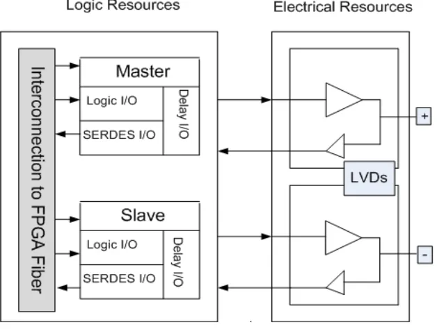
The I/O resources mean the interconnection of FPGA. It is provide extra automation software solutions for I/O design process and easier to I/O design are more flexible. All I/O’s are on the edge of the chip and it is grouped into some banks. Each bank has 30-40 I/O blocks and eight clock pins per edge. The differential receiver and on-chip termination is available in all banks. Each I/ O pair has two IO logic blocks as master and slave as shown in Figure 1. It can be operate independently. Every I/O logic block contains I/O serial to parallel or parallel to serial converter and DE-serializer (IOSERDES), IO delay and memory resources.
Figure 1. Block Diagram of I/O Resources
2.2 Logic Resources
The input lines go into the input and enable of lookup table. The output of the lookup table gives the result of the logic function that it implements in Figure 2. Lookup table is implemented using SRAM.
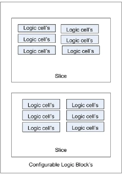
The CLB’s contained slices, logic cells, lookup table, flip-flops connected through intra-interconnect. The CLB’s access the interconnect fabric through Connection Block’s (CB’s) and CLB’s wire are interconnected through switch matrix blocks [6].
There are two types of slices in vertex-6 FPGAs like as sliceM and sliceL. SliceM is the full slice (25%) whose lookup table can be used for logic and memory. The sliceL is a logic and arithmetic slice (75%) only. Its lookup table can be used for logic not memory.
2.3 Clock Resources
Figure 2. (a) 4-input Lookup Table and Sets by Configuration Bit-Stream
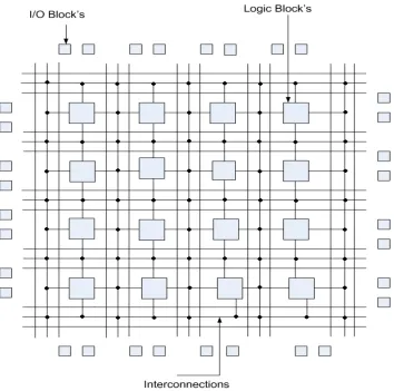
Figure 2b. Input/output Block’s, Configurable Logic Block’s and Interconnection of FPGA’s
3. Xilinx PlanAhead tool Using FPGA design flow and steps
Figure 2c. Internal structure’s of CLB’s for vertex-6
Figure 2d. CLB’s contains two slices
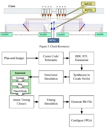
Figure 3. Clock Resources
Figure 4. PlanAhead Tool Based FPGA design Flow
In Figure 4, the implementation step process a netlist files which consists of translate, map and place & route phases. The translate step merge multiple design file into a single netlist. The map step group logical symbols from the netlist into physical components (Slice and IOBs) specific to target device. The place & route step place components onto the chip, connect through
Figure 6. FPGA design Technique using Duplicating Flip-flops process
the switch matrix as shown in Figure 2(d), dedicated routing lines and extract timing data into reports. These extracting reports contain design information like as timing analyzing, floorplanning, FPGA editing, X-powering, slacks histogram conditions etc. After completing this implementation and generate a bit (.bit extension file) file need to testing & verification through HDL simulator. When the design had been totally verified with exact timing, the final bit file will be generated. This bit file can be downloaded directly into the FPGA or through JTAG interface [7] and as shown in Figure 5.
Figure 8. Device package with blocks
Table 3. Implemented Design Report From Planahead Tool Figure 10. Edited arrays in FPGA
Table 1. Clock Regions
Figure 11. Interconnection and LUT utilization per CLB in FPGAs
Figure 12. Simulation results of output ASIC data
There is a various type of FPGA design techniques like as duplicating flip-flops, pipelining, I/O flip-flops, circuit synchronizations etc. One of the examples of duplicating flip-flops process in FPGA design technique, if high fan-out nets can be slow and hard to route, the duplicating flops can be fixed both problems and gives the better design trade-off. In Figure 6, the source flip-flops drives two register banks constrained to different region of the chip and the source flip-flip-flops has been duplicated.
4. Synthesis Techniques and Simulations
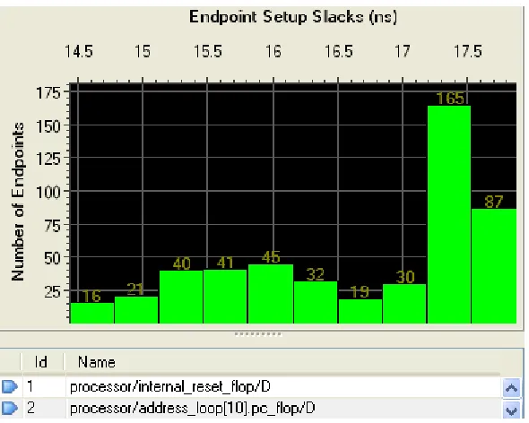
Synthesis includes generic optimization, slack optimizations, power optimizations followed by placement and routing. Implementation includes partition, place and route. The output of design implementation phase is bit-stream file. In Figure 7, the project manager manages sources, customize IP and view project details in the project summary. After synthesis, the flow manager includes report timing, slacks histogram in Figure 13, and chipScope pro utilities. The simulated gate arrays as shown in Figure 9 and Figure 10 which can be easily reconfigure, replace and interconnect by included Xilinx PlanAhead FPGA editor. The interconnection and LUT Utilization per CLB in FPGAs and Simulation Results of output ASIC data and VHDL module of activation process as shown in Figure 11 and Figure 12.
5. Implementation
Figure 13. Slacks Histogram Results Report
Constraint File) formats which need to netlist of integrated design, timing constraint, FPGA pin assignment in Figure 8 respectively. After synthesize, the clock resources, confidence level and implemented design report results are given in TABLE 1, 2 and 3. In Figure 11, Interconnection and LUT Utilization per CLB in FPGAs. The output waveforms are tested in ASIC VHDL module of activation process. Bit stream file is fed to a simulator which simulates the design functionality and reports errors in desired behavior of the design. Timing tools are used to determine maximum clock frequency of the design. Now the design is loading onto the target FPGA device and testing is done in real environment.
6. Conclusions
In this paper, we presented a new dynamic interconnection for reconfigurable in FPGAs and the basic concept of interconnection. Xilinx PlanAhead tool can be easily synthesis and presents good implemented results. The advantages of PlanAhead tools are high performance, flexibility, code processing speed and the possibility of dynamic resources placement of module at run-time.
7. Acknowledgment
This work was supported in part by the second stage of Brain Korea 21 Project in 2012 (NRF), World Class University (R32-2010-000-20014-0, NRF, Korea), Fundamental Research (2010-0020942, NRF), and Mid-career Researcher Program (National Leading Research Lab, 2012-002521, NRF and MEST) Republic of Korea.
References
[1] www.xilinx.com.
[2] Gaccione, S.A., Levi, D. (1999). The Advantage of Run-time Reconfiguration, In: Jhon Schewel et al editor, Reconfigurable Technology FPGA’s for computing and Application, In: proc. SPIE 3844, 87-92, Bellingham WA, Sep.
[3] Lysaght, P., Dunlop, J. (1993). Dynamic Reconfiguration of FPGA’s in W. Moore, W. Luk [Ed’s] more FPGA’s proceeding of the international workshop on Field Programmable Logic and Applications, 82-94.
[4] DiMicheli, G. (1994). Synthesis and optimization of Digital Circuits, McGraw-Hill.