64 INTERNATIONAL JOURNAL OF ADVANCES IN ENGINEERING RESEARCH
LOW POWER FULL ADDER USING GROUND BOUNCE
NOISE TECHNOLOGY
1
T. Praveen Kumar, 2Mr. R. Prithiviraj
1
Student, M.TECH( VLSI Design) SRM University, Chennai, India
2
Assistant Professor (O.G),
Department of Electronics and Communication SRM University,Chennai, India
ABSTRACT
Static leakage power consumption and ground bounce noise at nanometer scale are two important parameters, to keep in consideration are compactness and power which affects the performance of any VLSI circuits. Full adder is the vital part of digital circuits which employ arithmetic operation. Adder circuit is widely used in many digital circuits for arithmetic operation as well as an adder for address generation in many processors and microcontrollers. So we need to choose which one should be employed in large scale system at higher speed. It is necessary to make these systems more efficient so as to survive with high speed while consuming low power. As the speed of the circuit increases, the most unwanted parameter that is exhibited by the circuits is ground bounce noise .This paper here describes how the reduction of leakage power and ground bounce noise from the 14T full adder circuits can be made to make it more reliable to be used with high speed system. All the simulation in this paper has been carried out using tanner eda tool.
Keywords:- ground bounce noise, power consumption, variable body bias.
1.INTRODUCTION
65 INTERNATIONAL JOURNAL OF ADVANCES IN ENGINEERING RESEARCH
This paper describes proposed stacking power technique where we insert a sleep transistor between active ground rail and virtual ground. The main idea behind this technique is that the device is turned off in sleep mode and also the cut off leakage path provides a reduced leakage power with improved performance in power and reduced ground bounce noise using novel technique with improved stacking and power gating. Low power has emerged as a principal theme in today’s world of electronics industries [5]. Power dissipation has become an important consideration as performance and area for VLSI Chip design [4]. With shrinking technology reducing power consumption and over all power management on chip are the key challenges below 100nm due to increased complexity. For many designs, optimization of power is important as timing due to the need to reduce package cost and extended battery life. For power management leakage current also plays an important role in low power VLSI designs[2]. Leakage current is becoming an increasingly important fraction of the total power dissipation of integrated circuits [3]. An adder is one of the most critical components of a processor which determines its throughput, as it is used in the ALU, the floating-point unit, and for address generation in case of cache or memory access [6]. Recently there have been several attempts to design energy recovering logic in the pursuit of energy efficient circuitry. In this paper we are going to design a ultra low power 14 Transistor adder using the novel stacking power gating logic which has very low leakage power.
2.14T FULL ADDER:
66 INTERNATIONAL JOURNAL OF ADVANCES IN ENGINEERING RESEARCH
Fig:1 14T full adder
Fig:2 14T full adder with stacking power gating
2.1: GROUND BOUNCE NOISE
67 INTERNATIONAL JOURNAL OF ADVANCES IN ENGINEERING RESEARCH
capacitance between the PCB trace on the output pin and ground. The load capacitance, which varies with board design, is typically 50 pF. During logic level transitions, the rapid charging and discharging of CL results in an inductive L(di/dt) voltage drop across LPVCC and LPGND. Voltage drop across LPGND causes the IC ground potential to rise above the power supply ground potential. Other ICs may see this effect as a logic change on the output of the device. When the IC input returns high, ground bounce of the opposite polarity occurs due to the voltage drop across LPVCC.
2.2 VARIABLE BODY BIAS:
In statistics, omitted-variable bias (OVB) occurs when a model is created which incorrectly leaves out one or more important causal factors. The "bias" is created when the model compensates for the missing factor by over- or underestimating the effect of one of the other factors. More specifically, OVB is the bias that appears in the estimates of parameters in a regression analysis, when the assumed specification is incorrect in that it omits an independent variable that is correlated with both the dependent variable and one or more included independent variables.
68 INTERNATIONAL JOURNAL OF ADVANCES IN ENGINEERING RESEARCH
3. SIMULATION RESULTS:
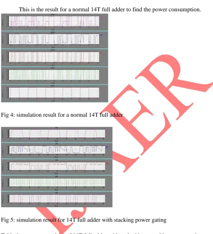
This is the result for a normal 14T full adder to find the power consumption.
Fig 4: simulation result for a normal 14T full adder
Fig 5: simulation result for 14T full adder with stacking power gating
Table:1 power comparison of 14T full adder with and without stacking power gating
Parameter 14T full adder
14T full adder with stacking power gating
69 INTERNATIONAL JOURNAL OF ADVANCES IN ENGINEERING RESEARCH
Average power
3.199e-11 (watts)
2.154e-11 (watts)
1.142e-11 (watts)
The average power for a 14T full adder with and without stacking power gating and variable body bias is observed in the above table.
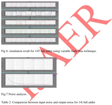
Fig 6: simulation result for 14T full adder using variable body bias technique.
Fig:7 Noise analysis.
Table 2: Comparison between input noise and output noise for 14t full adder
Frequency (Hz)
Input
noise(magnitude)
Output
noise(magnitude)
2.0e6 3.98e-6 1.19e-8
70 INTERNATIONAL JOURNAL OF ADVANCES IN ENGINEERING RESEARCH
4.17e6 1.91e-6 5.70e-9
5.02e6 1.58e-6 4.74e-9
6.03e6 1.32e-6 3.94e-9
7.26e6 1.10e-6 3.23e-9
The above table depicts the difference in the input noise and output noise obtained for 14T full adder. Here we vary the frequencies and find the magnitude of the input and output respectively.
4 CONCLUSION:
In this paper we proposed a modified 14T full adder for microprocessor and arithmetic logic circuit with low ground bounce noise and reduced leakage power. Here we have used high performance power gating technique to reduced active power and ground bounce noise. We had reduced the power consumption by 66.66 percent using variable body bias method and 33.33 percent decrease in power using stacking power gating method. Noise analysis is carried out for 14T full adder.
5. REFERENCES:
[1] Radu Zlatanovici, Sean Kao, Borivoje Nikolic, “Energy-Delay of Optimization 64-Bit Carry- Lookahead Adders With a 240ps 90nm CMOS Design Example,” IEEE J. Solid State circuits, vol.44, no. 2, pp. 569-583, Feb. 2009.
[2] K.Navi, O. Kavehei, M. Rouholamini, A. Sahafi, S. Mehrabi, N. Dadkhai, “Low-Power and
High-Performance 1-bit CMOS Full Adder Cell,” Journal of Computers, Academy Press, vol. 3, no. 2, Feb. 2008.
[3] Rabaey J. M., A. Chandrakasan, B. Nikolic, Digital Integrated Circuits, A Design Perspective, 2nd Prentice Hall, Englewood Cliffs, NJ, 2002.
[4] Pren R. Zimmermann, W. Fichtner, “Low-power logic styles: CMOS versus pass-transistor
logic,” IEEE J. Solid- State Circuits, vol. 32, pp. 1079–1090, July 1997.
[5] Tripti Sharma, K.G.Sharma, Prof.B.P.Singh, “High Performance Full Adder
71 INTERNATIONAL JOURNAL OF ADVANCES IN ENGINEERING RESEARCH
[6]Harmander Singh, Kanak Agarwal, Dennis Sylvester, Kevin J. Nowka,”Enhanced Leakage
Reduction Techniques Using Intermediate Strength Power Gating,”IEETransactions on VLSI Systems,Vol.15, No.11, November2007.
[7] Tripti Sharma, Prof.B.P.Singh, K.G.Sharma, Neha Arora Electronics & Communication Deptt. MITS Deemed University, Rajasthan INDIA, “High Speed, Low Power 8T Full Adder Cell with 45% Improvement in Threshold Loss Problem”, Recent Advances in Networking, VLSI and Signal Processing.