Published online February 6, 2015 (http://www.sciencepublishinggroup.com/j/jeee) doi: 10.11648/j.jeee.s.2015030201.25
ISSN: 2329-1613 (Print); ISSN: 2329-1605 (Online)
Evaluation of a new hybrid technique based on DTMOS and
PFA to improve supply voltage and power consumption of a
class-AB amplifier
Hossein Movahedi-Aliabad
1, *, Akram Norouzi
2, Sepideh Soltanmoradi
2, Mahshid Nasserian
3,
Manijeh Shahi
21
Department of Electrical and Electronics, Quchan Technical Institute, Technical and Vocational University, Quchan, Iran 2
Department of Electrical Engineering, Bojnourd Branch, Islamic Azad University, Bojnourd, Iran 3
Department of Electrical Engineering, Ferdowsi University of Mashhad, Mashhad, Iran
Email address:
[email protected] (H. Movahedi), [email protected] (A. Norouzi), [email protected] (S. Soltanmoradi), [email protected] (M. Nasserian), [email protected] (M. Shahi)
To cite this article:
Hossein Movahedi-Aliabad, Akram Norouzi, Sepideh Soltanmoradi, Mahshid Nasserian, Manijeh Shahi. Evaluation of a New Hybrid Technique Based on DTMOS and PFA to Improve Supply Voltage and Power Consumption of a Class-AB Amplifier. Journal of Electrical and Electronic Engineering. Special Issue: Research and Practices in Electrical and Electronic Engineering in Developing Countries.
Vol. 3, No. 2-1, 2015, pp. 66-71. doi: 10.11648/j.jeee.s.2015030201.25
Abstract:
In this paper, two useful techniques of Dynamic Threshold Voltage MOSFET (DTMOS) and Positive Feedback Amplifier (PFA) are investigated separately and are applied simultaneously on a Class-AB Amplifier in the 180 nm CMOS technology. In the first proposed technique, Simulation results show that operating voltage can be limited to ±0.5 V in which the voltage gain and bandwidth are 52.6 dB and 103.51 MHz, respectively. In the second proposed technique, the power consumption is reduced more than 50%, the open-loop gain is enhanced 47% and Common Mode Rejection Ratio (CMRR) improves to 86.5 dB. By applying combination of these two techniques for designing the amplifier, CMRR increases to 92.1 dB and the power consumption reduces to 97 µW with the bandwidth of 59.12 MHz.Keywords:
Class-AB Amplifier, DTMOS, FVF, PFA.1. Introduction
One of the most important parts of an electronic measurement system is its input section, (i.e., sensor). Detection of the desired input quantity and converting to an electrical signal is the most important part of such a system. Nowadays, due to decreasing supply voltage and power consumption of these circuits, achieving the minimum size and increasing lifetime of batteries, results in continuing designing electrical circuits with this approach [1].
New techniques of generation of energy from physical quantities such as light, temperature difference between two points, mechanical vibration frequency of components, moving variation, speed of rotation, etc in nanometer or micrometer scale leads to replacing batteries and power supplies with these new kinds of energy generators. Since the power provided by these generators is not high, use of low-power and low-voltage circuits is very important [2].
Hence, for detection of the desired quantities, designing operational amplifier (Op-Amp) and electronic circuits should be done with the goal of achieving high voltage gain in low operating voltage and power consumption. Applications such as portable and low power measurement systems, especially communication and wireless applications, exhibit importance of usage of low voltage and low power consumption circuits these systems [3].
In [4], Sarbishaei et al. use positive feedback for increasing the voltage gain. However, they couldn’t achieve low operating voltage and power supply. Also, in [5] Lopez-Martin et al., employ combination of local common mode feedback (LCMFB) and super class-AB OTA (operational transconductance amplifier) for increasing voltage gain and bandwidth in three circuits with different types of supply circuits in the internal stage.
techniques of dynamic threshold voltage MOSFET (DTMOS) and positive feedback amplifier (PFA) are used separately and their combination that is the main idea of this paper are applied on a class-AB operational amplifier. In continue, simulation results are compared with those reported in [4] and [5].
2. Theorem
Detecting and measuring required quantities and also minimizing the operating supply voltage leads to usage of energy provided by physical components in nanometers sizes. Fig. 1 shows the block diagram of a wireless sensor [3]. In this structure the required power for driving internal parts is provided by an electrical generator and is managed for usage of internal components of the sensor. Structure of the detection part and converting the input quantities to an electrical signal should be designed very well to operate in the following conditions:
When achieved voltage from energy generator is not enough.
When size of wireless sensor due to specific applications and low power should be decreased.
Hence using techniques for decreasing supply voltage is useful that are discussed in this paper later.
Fig. 1. Internal structure of a wireless sensor[3].
2.1. DTMOS Technique
Fig. 2. DTMOS internal structure in a CMOS Transistor [8].
DTMOS Technique has been proposed with the goal of decreasing Vthand off-state leakage current. However, it can
be used when transistor is in the saturation region. As seen in Fig. 2, in this technique the gate and body terminals are connected together and the input signal is applied to these terminals. If VBS>0, Vthdecreases according to (1).
F BS F th
th V V
V = 0+λ( 2φ − − 2φ (1)
in which VBS is source-body voltage of the transistor, Vth0is the
threshold voltage when VBS = 0, λ is the body effect coefficient,
φF is the Fermi potential (that has a value between 0.3 to 0.4 V)
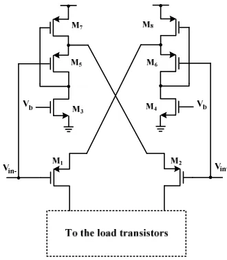
[7]. In Fig. 3, the input signal is applied to the gate and body terminals of M1 and M2 which are biased in DTMOS structure.
Fig. 3. DTMOS structure used in an Op-Amp input stage
Since lower voltage (compared to the case input signals are applied to the gates of transistors) is needed for driving transistors, we expect that input voltage range increases in the common mode and also the bias current decreases, resulting in saving power [8-9].
2.2. Positive Feedback Amplifier (PFA)
There are different techniques for increasing the output impedance and voltage gain such as cascading transistors, Gain Boosting and Positive Feedback Amplifier (PFA). In the first and second approaches, at least extra four transistors are needed and voltage swing is limited. Hence, these techniques cannot be employed in low voltage applications [10].
In the PFA technique, due to achieving negative conductance coefficient and also high output impedance, we can expect maximum output voltage swing and high DC voltage gain [11].
Fig. 4 shows the structure of a differential PFA. Equivalent circuit for this circuit, is presented in Fig. 5. In this schematic, feedback factor is gm2 and the closed-loop gain can calculated
as following:
) 1 ( )
(
OL OL
mi CL
CL A
A g vi vo
A = = −β (2)
feedback used in the Op-Amp [4].
Fig. 4. Schematic of a differential PFA
Fig. 5. Half equivalent circuit of a differential PFA
To achieve high gain, this factor can be used as following:
oi o o m
OL g g g g
A = 1+ 1+ 2+
β (3)
It is worth mentioning that using this technique, high gain can be achieved without using cascading technique or cascading amplifier stages. Also, there is no need to the common mode feedback (CMFB) due to combination of M4
and M5.
2.3. Flipped Voltage Follower (FVF)
A simple Flipped Voltage Follower (FVF) configuration is seen in Fig. 6. This structure can be used as a voltage shifter or buffer. In this structure, the output current depends on the current passing through the main input transistor (MFVF).
Hence, by approaching to VSG(MFVF), the gain becomes 1 [4].
Fig. 6. Simple FVF structure
The most important feature of this structure is its low output impedance (20 to 100 Ω) that makes it suitable for use in negative feedback structures [5]. This structure can be employed as the input stage in an Op-Amp that is shown in Fig. 7. In this circuit, current passing through M2 increases when
Vi->Vi+. In this case, the gate voltage of M2 decreases due to
reducing Vi+, while its source voltage increases from another
path. If this structure used in the input stage, it can increase slow rate of the amplifier.
Fig. 7. FVF structure of an Op-Amp input stage
2.4. Super Class-AB OTA
Fig. 8 shows a Class-AB OTA. In this circuit, LCMFB is used for current stabilizing in main transistors. In order to increase bandwidth of the circuit and slow rate, two resistors are used in this structure [2]. Combination of M4 and M5 cause
these transistors to operate in the ohmic region. Slow rate nan calculated by SR = IBias /CL. For incraesing the solw rate, we
need to increase IBias which leads to more power dissipation. If
this current is choosen low, the static power decreases. Size of R1 and R2 should be selected such that suitable phase margin is
achieved. Using this technique, Autors in [4] can improve the slow rate 3 times compared to a conventional OTA.
When common mode (CM) input is applied in this circuit, current passing through resistors becomes zero and voltage of M3 nad M6 becomes equal. In this condition, IBias is devided
between M1 and M2 equal. If differntial input is applied to the
circuit, the currents of resistors and hence voltage of X and Y nodes become different.
When Vi=V(i+)-V(i-) is applied and Id=I1-I2 is generated, a
current is produced throughout resistors. Maximum difference between X and Y nodes can be calculated by:
2
Bias MAX
GS RI
V =
∆ (4)
Calculated voltage difference in the above equation produces maximum voltage swing in current of the output stage. DC open-loop gain can be writhen as:
out m Y m
OpenLoop g R g R
A = 2 6 (5)
in which RY is impedance of the Y node and Rout is impedance
of the output node. Also, RY can be expressed by:
2 5 o
o r
r R
RY= (6)
Furthermore, resistor R can determine the maximum output current that is:
2 5
,
4 )
( DS GSMAX
Max
Out V V
I =β +∆ (7)
It is worth mentioning that in the differential mode, gates of M4 and M5 are grounded and parasitic capacitances don’t
affect X and Y nodes. In Fig. 8, generated differential current is proportional to Vid2[11-12]. Also the output current is
proportional to Id2 and hence, it is proportional to Vid2.
Therefore the proposed circuit is a super class-AB OTA [13]. In this paper, two useful techniques of PFA and DTMOS are investigated separately and then are applied simultaneously on the implemented super class-AB OTA in the 0.18 µm CMOS technology. In order to make comparison fair, figure of merit (FOM) is calculated as follows:
Supply d
OpenLoop
V P
GBW A
FOM = . . 1 (8)
in which GWB is production of gain and bandwidth and AOpenLoop is open-loop gain[14].
3. Circuit Implementation
For simulating the proposed structure, first a differential class-AB OTA, -in which FVF technique is used- is implemented in the 0.18 µm CMOS technology using Hspice software. Then DTMOS technique is applied to the first stage. In this case, operating voltage is limited to ±0.5 V. Bias currents are selected 2 µA. Then without using DTMOS technique, M4 and M5 transistors along with R1 and R2 are
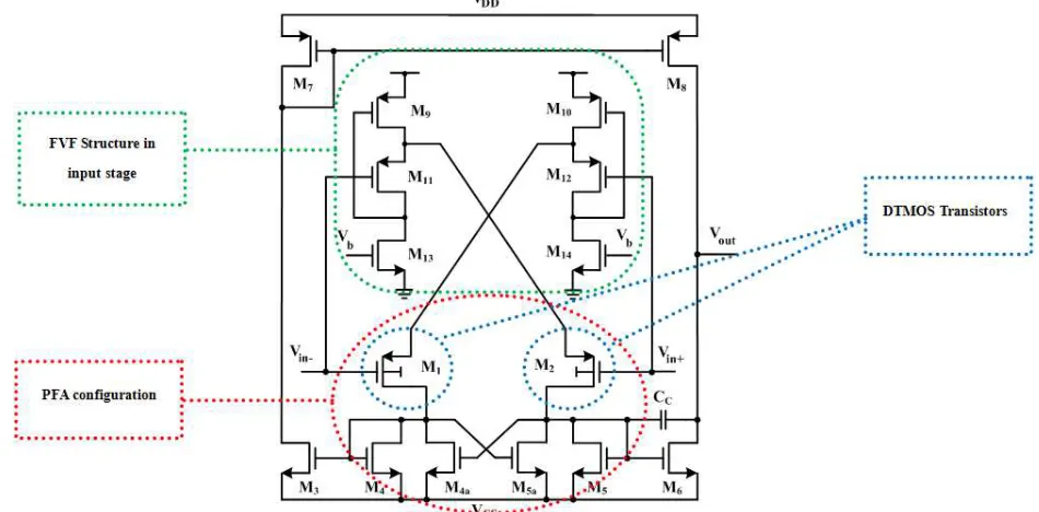
replaced by PFA and simulation is carried out again. In this case supply voltage is ±1 V. The proposed technique in this paper is combination of two stated techniques. Using the proposed structure supply voltage can be limited to ±0.5 V and many circuit parameters are improved. Fig. 9 shows circuit of the proposed structure.
Fig. 9. Schematic of the proposed circuit. Structure of the super class-AB OTA in which DTMOS and PFA techniques are used.
4. Simulation Results
Circuits explained in the previouse section are simulated
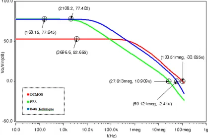
When PFA technique is used for implementing the amplifier, the power consumption reduced more than 50%, the voltage gain improves more than 47%, and CMRR enhances to 86.5 dB.The open-loop gain and bandwidth of the proposed circuit are 77.4 dB and 59.12 MHz, respectively in which the supply
voltage is ±0.5 V. Table 1 shows simulation results of DTMOS, PFA and the proposed structures and also techniques proposed in [4] and [5] (in which three bias float circuits (A), (B), and (C) are used). As observed in Table 1, the proposed circuit has the best CMRR, least power and the best FOM.
Fig. 10. Voltage gain cuves of DTMOS, PFA and the proposed technique.
Table 1. Comparison of different techniques parameters.
This Work Simulated [5]-(A) circuit
in this paper [5] (C) [5] (B) [5] (A) [4] Parameter Proposed PFA DTMOS 0.18 0.18 0.18 0.18 0.5 0.5 0.5 0.18 Technology (µm) ±0.5 ±1 ±0.5 ±1 ±1 ±1 ±1 1.8
VSupply (V)
2 2 2 10 10 10 10
--IBias (µA)
59.12 27.6 103.51 22.1 0.47 0.41 0.725 69 GBW (MHz) 77.4 77.64 52.6 50 37.5 37.5 43 83.7 Gain (dB) 88 85 89 90 90 90 90 87
Phase Margin (º)
92.1 86.5 63.2 52.1 69 70 68 --CMRR (dB) ±0.4 ±0.85 ±0.45 ±0.85 -- -- -- 1.6 Output Swing (V)
2 2 2 5 80 80 80 2
Load Capacitor (pF)
9.5 12 8 6.5 252 230 230 --
Output Noise (µVrms)
97 112 248 280 140 120 120 450 Power (µW) 98-86 80-84 98-80 86-81 57-46 50-53 55-58 --
PSRR(+ , -) (dB)
105 -44.5 450 -177 148.4 -50 203 -86.5 42 -80 92 -76 100 -78 226 ---Slew Rate +/- (V/µS)
47.17 9.56 21.95 1.975 0.063 0.064 0.13 7.12 FOM*
* FOM : Figure of Merit
5. Discussion and Conclusion
In this paper, two practical techniques of DTMOS and PFA are investigated separately and are applied simultaneously on a Class-AB Amplifier in the 180 nm CMOS technology. In the first proposed technique, Simulation results show that
operating voltage can be limited to ±0.5 V in which the voltage gain and bandwidth are 52.6 dB and 103.51 MHz, respectively. In the second proposed technique, the power consumption is reduced more than 50%, the open-loop gain is enhanced 47% and CMRR improves to 86.5 dB.
the amplifier, CMRR increases to 92.1 dB and the power consumption reduces to 97 µW with the bandwidth of 59.12 MHz.
Simulation result provided in the previous section proves that the proposed circuit improves many parameters of the amplifier. Decreasing operating voltage, power consumption and enhancing parameters including voltage gain, bandwidth and CMRR make the proposed structure a good choice for implementing high gain amplifiers with minimum voltage supply and also low-power portable and wireless applications.
References
[1] P. K. Sinha, A. Vikram and Dr. K. S. Yadav, "Design Of Two Stage CMOS Op-Amp With Low Power And High Slew Rate", International Journal of Engineering Research & Technology, Vol. 1 Issue 8, ISSN: 2278-0181, 2012.
[2] L. W. Zhong, Zh. Guang, Y. Ya, W. Sihong and C. Pan, "Progress in nanogenerators for portable electronics", Materials today from Elsevier Journals, Vol. 15, No. 12, pp. 532-543, 2012.
[3] A. Nechibvute, A. Chawanda and P. Luhanga, "Piezoelectric Energy Harvesting Devices: An Alternative Energy Source forWireless Sensors", Hindawi Publishing Corporation, Smart Materials Research, Article ID 853481, 13 pages, DOI :10.1155/2012/853481, 2012.
[4] H. Sarbishaei, T. K. Toosi, E. Z. Tabasy and R. Lotfi, "A High-Gain High-Speed Low-Power Class -AB Operational Amplifier", 48th IEEE International Midwest Symposium on Circuits and Systems, Vol. 1, pp. 271 - 274 , 2005.
[5] J. López-Martín, S. Baswa, J. Ramirez-Angulo and R. G. Carvajal, "Low-Voltage Super Class AB CMOS OTA Cells With Very High Slew Rate and Power Efficiency", IEEE Journal Of Solid-State Circuits, Vol. 40, No. 5, pp. 1068-1077, 2005.
[6] S. Baswa, M. Bikumandla, J. Ramírez-Angulo, A. J.
López-Martín, R. G. Carvajal and G. Ducoudray-Acevedo, "Low-Voltage Low-Power Super Class-AB CMOS Op-Amp with Rail-to-Rail Input/Output Swing", 5th IEEE International Caracas Conference on Devices, Circuits and Systems, Vol. 1, pp. 83-86, 2004.
[7] Lasanen and Kimmo, "Integrated analogue CMOS circuits and structures for heart rate detectors and other low-voltage, low-power applications", University of Oulu, Oulu, Finland, 2011.
[8] S. Izadpanah-Tous, M. Behroozi and V. Asadpoor, "Design of 0.4 V operational amplifier using low-power techniques", Majlesi Journal of Telecommunication Devices, Vol. 2, No. 1, pp. 145-149, 2012.
[9] L. Qiang, T. Kuo Hwi Roy, H. Teo Tee and S. Rajinder, "A 1-V 36-µW Low-Noise Adaptive Interface IC for Portable Biomedical Applications", IEEE European Solid-State Device Research Conference, 11-13 September 2007.
[10] K. Bult and G. Geelen, "A Fast-Settling CMOS Op Amp for SC Circuits with 90-dB DC Gain", IEEE J. Solid-state Circuits, Vol. 25, No. 6, pp. l379-1384, 1990.
[11] S. Voldman, D. Hui, D. Young, R. Williams, D. Dreps, J. Howard, M. Sherony, P. Assaderaghi and G. Shahidi, "Silicon-on-insulator dynamic threshold ESD networks and active clamp circuitry", Electrical Overstress/Electrostatic Discharge Symposium, pp. 29-40, 2000.
[12] J. Ramirez-Angulo, R. G. Carvajal, A. Torralba, J. Galan, A. P. Vega-Leal and J. Tombs, "The Flipped Voltage Follower: A useful cell for low-voltage low-power circuit design", in Proc. ISCAS 2002, Scottsdale, AZ, pp. II 615-618, 2002.
[13] M. M. Amourah and R. L. Geiger, "A High Gain Strategy With Positive-Feedback Gain Enhancement Technique", IEEE International Symposium on Circuits and Systems, Vol. 1, pp. 631- 634, 2001.
![Fig. 1 shows the block diagram of a wireless sensor [3]. In this](https://thumb-us.123doks.com/thumbv2/123dok_us/9872494.1974708/2.595.346.497.228.409/fig-shows-block-diagram-wireless-sensor.webp)