CURRENT SOURCES
by
Sulmer A. Fernández Gutierrez
A dissertation
submitted in partial fulfillment of the requirements for the degree of
Doctor of Philosophy in Electrical and Computer Engineering Boise State University
DEFENSE COMMITTEE AND FINAL READING APPROVALS
of the dissertation submitted by
Sulmer A. Fernández Gutierrez
Dissertation Title: Simulation of a Magnetron Using Discrete Modulated Current Sources
Date of Final Oral Examination: 12 March 2014
The following individuals read and discussed the dissertation submitted by student Sulmer A. Fernández Gutierrez, and they evaluated her presentation and response to questions during the final oral examination. They found that the student passed the final oral examination.
Jim Browning, Ph.D. Chair, Supervisory Committee
Kris Campbell, Ph.D. Member, Supervisory Committee
Wan Kuang, Ph.D. Member, Supervisory Committee
Mark Gilmore, Ph.D. External Examiner
iv
v
I would like to thank Dr. Jim Browning for serving as my major professor and guide through my Ph.D. program. It was a pleasure to be his first Ph.D. student; I truly appreciate all the time and advice he gave me throughout my time at Boise State
University. The enthusiasm he has for his research was motivational and encouraging for me, even during tough times in the Ph.D. pursuit. Thanks for all the valuable insights and support, which were a major contribution to complete this dissertation. I would also like to thank Dr. Kris Campbell, Dr. Wan Kuang, and Dr. Mark Gilmore for being willing to serve as members of my committee. I would also like to acknowledge all the faculty and staff that I worked with at Boise State University, took classes from, and met throughout my graduate studies. They were wonderful people and a real pleasure to know. I also acknowledge the funding sources that made my Ph.D. work possible. The first year this research was funded by the Air Force Office of Scientific Research (ASFOR) under Contract No. FA9550-09-C-0141. The remaining time to completion was funded by the Electrical and Computer Engineering (ECE) Department at Boise State University.
vi
time you took speaking with me, and overall friendliness.
Thank you to my MVEDs research group: Peter, Marcus, and Tyler, you were always open for discussion, helping me find errors, and checking my work. I appreciate your assistance and friendship. Although, we worked in different projects, we were always able to collaborate with each other.
vii
Magnetrons are microwave oscillators and are extensively used for commercial and military applications requiring power levels from the kilowatt to the megawatt range. It has been proposed that the use of gated field emitters with a faceted cathode in place of the conventional thermionic cathode could be used to control the current injection in a magnetron, both temporally and spatially. In this research, this concept is studied using the 2-D particle trajectory simulation Lorentz2E and the 3-D particle-in-cell (PIC) code VORPAL. The magnetron studied is a ten cavity, rising sun magnetron, which can be modeled easily using a 2-D simulation. The 2-D particle trajectory code is used to model the electron injection from gated field emitters in a slit type structure, which is used to protect the gated field emitters. VORPAL is used to study the magnetron performance for a cylindrical, a five-sided, and a ten-sided cathode. Finally, VORPAL is used to simulate a modulated, addressable, ten-sided cathode. The aspects of magnetron performance for which improvements are desired include mode control, efficiency, start oscillation time, and phase control. The simulation results show that the modulated, addressable cathode reduces startup time from 100 ns to 35 ns, increases the power density, controls the RF phase, and allows active phase control during oscillation.
viii
DEDICATION ... iv
ACKNOWLEDGEMENTS ... v
ABSTRACT ... vii
LIST OF TABLES ... xi
LIST OF FIGURES ... xii
CHAPTER ONE: INTRODUCTION ... 1
1.1 Overview and Introduction ... 1
1.2 Motivation and Contributions ... 5
1.3 Dissertation Organization ... 6
CHAPTER TWO: BACKGROUND... 8
2.1 Magnetron Operating Characteristics ... 8
2.2 Cylindrical Magnetron ... 12
2.3 Magnetron Resonant Circuit and Modes of Operation ... 14
2.4 The Hartree and Hull Cutoff Condition ... 17
2.5 The Diocotron Instability ... 19
2.6 Stability and Mode Separation ... 22
CHAPTER THREE: LORENTZ2E SIMULATION ... 30
3.1 Overview ... 30
ix
3.4 Electron Trajectory Analysis ... 34
3.5 Sensitivity Simulations ... 35
CHAPTER FOUR: LORENTZ2E SIMULATION RESULTS ... 37
4.1 Overview ... 37
4.2 Energy Distribution Analysis ... 37
4.3 Electron Velocity ... 39
4.4 Sensitivity Simulations ... 41
4.5 Summary of Results ... 54
CHAPTER FIVE: VORPAL SIMULATION SETUP ... 56
5.1 Overview ... 56
5.2 Software ... 56
5.3 Finite Difference Time Domain (FDTD) Technique ... 57
5.4 Numerical Stability ... 60
5.5 Boundary Conditions ... 61
5.6 Dey-Mittra Cut Cell Algorithm ... 62
5.7 Integration of the Equations of Motion ... 64
5.8 Modeling of a 2-D Ten Cavity Rising Sun Magnetron ... 64
5.9 Simulation Setup and Procedures ... 67
5.10 Rising Sun Magnetron Model with a Continuous Current Source ... 73
5.11 Rising Sun Magnetron Model with Modulated, Addressable, Current Sources ... 81
x
6.2 Continuous Current Source Model: Cylindrical Cathode ... 88
6.3 Continuous Current Source Model: Five-Sided Faceted Cathode ... 92
6.4 Continuous Current Source Model: Ten-Sided Faceted Cathode ... 99
6.5 Summary of Results ... 102
CHAPTER SEVEN: VORPAL SIMULATION RESULTS FOR THE MODULATED, ADDRESSABLE CATHODE ... 103
7.1 Overview ... 103
7.2 Modulated Five-Sided Faceted Cathode ... 103
7.3 Modulated Five-Sided Faceted Cathode with Time Overlap ... 106
7.4 Modulated Five-Sided Cathode with Time Overlap and DC Hub ... 110
7.5 Modulated Ten-Sided Faceted Cathode... 114
7.6 Modulated Ten-Sided Faceted Cathode with DC Hub ... 118
7.7 Modulated Ten-Sided Faceted Cathode with Active Phase Control ... 124
7.8 Summary of Results ... 130
7.9 Discussion of Application of Modulated Addressable Cathode ... 131
CHAPTER EIGHT: SUMMARY AND CONCLUSIONS ... 134
REFERENCES ... 138
APPENDIX A ... 152
Lorentz2E Simulations ... 152
APPENDIX B ... 173
xi
Table 3.1: Lorentz2E Magnetron Model Sensitivity Simulations. ... 36 Table 4.1: Voltage sensitivity analysis results for variations in the pusher electrode
voltage... 43 Table 4.2: Voltage sensitivity analysis results for variations in the emitter voltage. . 45 Table 4.3: Voltage sensitivity analysis results for variations in the pusher electrode
voltage with a pusher electrode thickness of 1.70 µm... 48 Table 4.4: Voltage sensitivity analysis results for variations in the emitter voltage
with a pusher electrode thickness of 1.7 µm. ... 50 Table 4.5: Voltage sensitivity analysis results for variations in the pusher electrode
voltage with a pusher electrode thickness of 0.4475 µm. ... 52 Table 4.6: Voltage sensitivity analysis results for variations in the emitter voltage
with a pusher electrode thickness of 0.4475 µm. ... 54 Table 5.1: Rising sun magnetron dimensions for cylindrical, five and ten-sided
faceted cathodes. ... 67 Table 5.2: Rising sun magnetron: cylindrical cathode VORPAL simulations. ... 80 Table 5.3: Rising sun magnetron: faceted cathode VORPAL simulations. ... 80 Table 5.4: Five-Sided Faceted Cathode Additional Simulation Tests with
Modulated, Addressable Current Sources. ... 87 Table 7.1: Current densities, power densities, and efficiencies for various cathode
xii
Figure 1: Power versus frequency performance of various microwave oscillator tubes, including backward wave oscillators (BWO) and voltage tunable
magnetrons (VTM). ...2
Figure 2: Microwave oven. ...3
Figure 3: Microwave radar transmission. ...4
Figure 4: Early type of magnetron: Hull original diode. ...8
Figure 5: Electron motion in a crossed electric and magnetic field diode configuration showing a cycloidal orbit. ...9
Figure 6: First 10-cm cavity magnetron. The slow wave circuit consists of 6 cavities. ... 11
Figure 7: Cross section of a magnetron showing reentrant cavities, with rc and ra the cathode and anode radii, and rv the vane radius. ... 12
Figure 8: Schematic diagram of a cylindrical magnetron. ... 13
Figure 9: Various forms of the anode block in a magnetron: (a) Slot type, (b) Vane type, (c) Rising sun, and (d) Hole-and-Slot type... 14
Figure 10: Equivalent circuit of an eight-cavity magnetron. ... 15
Figure 11: Lines of Force in π-mode of Eight-Cavity Magnetron. ... 17
Figure 12: Hartree threshold voltage diagram for an eight-cavity ... 19
Figure 13: Formation of the spoke-like electron cloud in a ten-cavity rising sun magnetron from VORPAL simulation. ... 20
Figure 14: Physical mechanism of the diocotron instability... 21
Figure 15: Strapping technique. Alternate anode segments at same potential. ... 23
xiii
Figure 18: Sixteen-cavity rising sun magnetron from Ostron Technologies [64]. ... 25 Figure 19: Proposed ten-cavity rising sun magnetron with a five-sided faceted
cathode. Each plate would have hundreds of slits with gated emitters beneath. ... 29 Figure 20: (a) Shielded cathode slit. Showing the stacked lateral field emission tips
on each side of the slit, a pusher electrode, the sole electrode (cathode plate), and the electron trajectories. (b) Faceted cathode showing slits. ... 32 Figure 21: Lorentz2E model of the shielded cathode slit structure. (a) The emitters on
each side, a field emission gate transparent to electrons, a pusher
electrode, the sole electrode, the electrode voltages, and the dimensions; and, (b) the electron ray trajectories ... 32 Figure 22: Magnetron model used in Lorentz2E. Five-sided cathode with a smooth
dummy anode showing electron ray traces from a single shielded slit structure on the left hand side of the top facet. ... 34 Figure 23: Transverse energy distribution from Lorentz2E for 200 electron rays. .... 38 Figure 25: Velocity in the x-direction versus position for 200 electron rays. ... 40 Figure 26: Velocity in the y-direction versus position for 200 electron rays. ... 40 Figure 27: Pusher Electrode Voltage at -22.20 kV. Emitter Voltage at (a) -22.20kV,
(b) -22.26 kV, (c) -22.34 kV, and (d) -22.5 kV... 42 Figure 28: Emitter voltage versus current ratio. ... 43 Figure 29: Emitter Voltage at -22.20 kV. Pusher Electrode Voltage at (a) -22.20 kV,
(b) -22.26 kV, (c) -22.34 kV, and (d) -22.5 kV... 44 Figure 30: Pusher electrode voltage vs. current ratio. ... 45 Figure 31: Pusher Electrode Voltage at -22.20 kV. Emitter Voltage at (a) -22.20 kV,
(b) -22.26 kV, (c) -22.34 kV, and (d) -22.5 kV. Pusher Electrode
Thickness of 1.70 µm. ... 47 Figure 32: Emitter voltage vs. current ratio at different pusher electrode voltages. ... 48 Figure 33: Emitter Voltage at -22.20 kV. Pusher Electrode Voltage at (a) -22.20 kV,
(b) -22.26 kV, (c) -22.34 kV, and (d) -22.5 kV. Pusher Electrode
xiv
Figure 35: Pusher Electrode Voltage at -22.20 kV. Emitter Voltage at (a) -22.20 kV,
(b) -22.26 kV, (c) -22.34 kV, and (d) -22.5 kV... 51
Figure 36: Emitter voltage vs. current ratio at different pusher electrode voltages. ... 52
Figure 37: Emitter Voltage at -22.20 kV. Pusher Electrode Voltage at (a) -22.20 kV, (b) -22.26 kV, (c) -22.34 kV, and (d) -22.5 kV... 53
Figure 38: Pusher electrode voltage vs. current ratio at different emitter voltages. ... 54
Figure 39: Yee model for placing fields on the grid. ... 59
Figure 40: Basic flow for implementation of Yee FDTD scheme without including particle injection. ... 60
Figure 41: Area fractions borrowed by cut cells in the Zagorodnov boundary algorithm. ... 63
Figure 42: Cylindrical cathode used in VORPAL simulations. ... 66
Figure 43: Five-sided faceted cathode used in VORPAL simulations. ... 66
Figure 44: Ten-sided faceted cathode used in VORPAL simulations... 67
Figure 45: Startup time of a typical magnetron simulation in VORPAL for the cylindrical cathode (Vca= -26.0 kV, B= 0.12 T, and Ja = 500 A/m). Stable oscillation is observed around 300 ns. ... 68
Figure 46: Linear current density vs. time for the cylindrical cathode, typical VORPAL simulation with B field = 0. ... 69
Figure 47: Anode linear current density vs. time during device operation for the cylindrical cathode, typical VORPAL simulation. ... 70
Figure 48: Rising sun magnetron cavity power diagnostic location. ... 71
Figure 49: Rising sun magnetron spoke formation. ... 72
Figure 50: Fast Fourier Transform (FFT) of the cavity voltage versus frequency. .... 74
xv
versus time, (b) Cavity voltage amplitude versus time from VORPAL, for the cylindrical cathode Vca = -26.0 kV, B = 0.12 T, and J'e = 500 A/m.76 Figure 53: Cathode-anode voltage versus time for the cylindrical cathode model
from VORPAL. ... 77 Figure 54: Rising sun magnetron simulation with particles after oscillations start and
spokes form. ... 78 Figure 55: (a) Temporal and spatial modulation concept of the current injection,
showing electrons being injected in phase with spokes. (b) Detailed view of one of the facets showing the ON and OFF emitters. ... 83 Figure 56: Modulated current overlap time diagram for the five-sided faceted
cathode. This diagram shows an example with 5 emitters in 1 facet (1 RF period). ... 86 Figure 57: Cylindrical cathode model from VORPAL simulation showing the RF
B-field and π-mode. This result corresponds to Vca = -26.0 kV, B = 0.12 T, and J’e = 500 A/m. ... 90
Figure 58: Cylindrical cathode cavity voltage frequency versus time with moving window, showing the startup time of the device at 300 ns, and the mode switching from 650 MHz to the Operating Frequency (π-mode) 960 MHz from VORPAL. ... 90 Figure 59: Cylindrical cathode Fast Fourier Transform (FFT), over entire simulation
time, of the loaded cavity voltage from VORPAL simulation. This plot clearly indicates that the π-mode is dominant at the frequency of operation of 960 MHz. ... 90 Figure 60: Cylindrical cathode VORPAL simulation results for Vc = -26.0 kV, B =
0.12 T, and J’e = 500 A/m. The red dots indicate electron macroparticles.
Figure 61(a) is at 0.012 ns, before oscillation, and Figure 61(b) is at 276 ns, after oscillation starts and the model is stable. ... 91 Figure 61: Cylindrical cathode continuous total emitted linear current density versus
time with no applied magnetic field (B=0). ... 91 Figure 62: Cylindrical cathode continuous anode linear current density during device operation versus time. ... 91 Figure 63: Cylindrical cathode (Vca = -22.2 kV, B = 0.09 T, J'e= 326 A/m)
xvi
Figure 65: Five-sided faceted cathode model from VORPAL simulation showing the RF B-field and π-mode. This result corresponds to Vca = -22.2 kV, B = 0.09 T, and J’e = 326 A/m. ... 93
Figure 66: Five-sided faceted cathode cavity voltage frequency versus time with moving window, showing the startup time of the device at 200 ns, and the mode switching from 650 MHz to the operating frequency (π-mode) 957 MHz from VORPAL. ... 94 Figure 67: Five-sided faceted cathode Fast Fourier Transform (FFT), over entire
simulation time, of the loaded cavity voltage from VORPAL simulation. This plot indicates that the π-mode is dominant at the frequency of
operation of 957 MHz. ... 94 Figure 69: Comparison of ICEPIC model versus VORPAL model. Vca = -22.2 kV, B
= 0.09 T, and J’e= 326 A/m. The top figures show the cylindrical
cathode model, the middle figures show the five-sided faceted cathode, and the bottom figures show the ten-sided faceted cathode. ... 96 Figure 70: Five-sided faceted cathode continuous total emitted linear current density
versus time with no applied magnetic field (B=0) . ... 98 Figure 71: Five-sided faceted cathode continuous anode linear current density during device operation versus time. The periodic current spikes are followed by spoke collapse. ... 98 Figure 72: Five-sided faceted cathode showing the transition of the spokes during the current instability. Spokes are shown (a) before current spike at 119.8 ns, (b) at current spike at 121.32 ns, and (c) after spokes collapse at 143.5 ns. ... 98 Figure 73: Ten-sided faceted cathode model from VORPAL simulation showing the
RF B-field and π-mode. This result corresponds to Vca = -22.2 kV, B = 0.09 T, and J’e = 326 A/m. ... 99
Figure 74: Ten-sided faceted cathode cavity voltage frequency versus time with moving window, showing the startup time of the device at 110 ns, showing the operating frequency (π-mode) at 957 MHz from VORPAL. ... 100 Figure 75: Ten-sided faceted cathode Fast Fourier Transform (FFT), over entire
xvii
frequency of operation of 957 MHz. ... 100 Figure 76: Ten-sided faceted cathode continuous total emitted linear current density
versus time with no applied magnetic field (B=0). ... 101 Figure 77: Ten-Sided faceted cathode continuous anode linear current density during
device operation versus time. ... 101 Figure 78: Five-sided faceted cathode showing discrete current sources setup for (a)
0.0987 ns and (b) 0.197 ns. There are five emitters per facet. All emitters are ON at the same time. ... 104 Figure 79: Five-sided faceted cathode with modulated, addressable current sources,
with B field turned OFF. This shows the emitters turning ON in sequence. The diagrams show one RF period, τRF=1.04 ns, Δt = 1/5 τRF. Frequency of modulation is 957 MHz. ... 105 Figure 80: Five-sided faceted cathode with modulated, addressable current sources.
The frequency of modulation is 957 MHz, τRF=1.04 ns, Δt = 1/5 τRF. .... 107 Figure 81: Five-sided faceted cathode with modulated, addressable current sources
plus current overlap. This diagram shows the case for current overlap of 25%. The frequency of modulation is 957 MHz, τRF = 1.04 ns, Δt = 1/5 τRF, τov = 0.0520 ns. ... 108 Figure 82: Modulated total emitted linear current density versus time with no applied magnetic field (B=0) for five-sided faceted cathode with 25% overlap. 109 Figure 83: Modulated anode linear current density versus time during device
operation for the five-sided faceted cathode with 25% overlap, showing current spike at around 102 ns. ... 109 Figure 84: Transition of the spokes during the current instability for the modulated,
addressable current sources for the five-sided faceted cathode with 25% overlap. Spokes are shown (a) before current spike at 110.3 ns, (b) at current spike at 113.1 ns, and (c) after spokes collapse at 116.3 ns. ... 109 Figure 85: Fast Fourier Transform (FFT) of the loaded cavity voltage from VORPAL
Simulation for the modulated, addressable, current source for the five-sided faceted cathode with 25% overlap. This plot indicates that the π-mode is dominant at the frequency of operation of 957 MHz. ... 110 Figure 86: Five-sided faceted cathode with modulated, addressable current sources
xviii
this is in an interchangeable feature in VORPAL. Green electrons were chosen to be seen on top to demonstrate the filled up gaps presented with only modulated and overlap technique. ... 112 Figure 87: Five-sided faceted cathode showing: on the left column the modulated
plus current overlap (25% overlap) simulation electrons and on the right the DC hub (5% J’e) electrons. It shows the comparison between the two,
and it can be seen that the gaps are filled by the green DC hub electrons. ... 113 Figure 88: Ten-Sided Faceted cathode showing discrete current sources setup for (a)
0.0163 ns and (b) 0.326 ns. There are three emitters per facet. All emitters are ON at the same time. ... 114 Figure 89: Ten-sided faceted cathode with modulated, addressable current sources,
with B field turned OFF. This shows the emitters turning ON in sequence. The diagrams show one RF period (two facets), τRF=1.04ns, Δt = 1/6 τRF. Frequency of modulation is 957 MHz. ... 115 Figure 90: Ten-sided faceted cathode with modulated, addressable current sources.
The frequency of modulation is 957 MHz, τRF=1.04 ns, Δt = 1/6 τRF. .... 116 Figure 91: Modulated total emitted linear current density versus time with no applied
magnetic field (B=0) for ten-sided faceted cathode. ... 117 Figure 92: Modulated anode linear current density versus time during device
operation for the ten-sided faceted cathode. ... 117 Figure 93: Modulated ten-sided faceted cathode cavity voltage frequency versus
time with moving window, showing the startup time of the device at 50 ns showing the operating frequency (π-mode) at 957 MHz from VORPAL. ... 118 Figure 94: Fast Fourier Transform (FFT), over entire simulation time, of the loaded
cavity voltage from VORPAL simulation for the modulated, addressable, current source, ten-sided faceted cathode. This plot indicates that the π-mode is dominant at the frequency of operation of 957 MHz. ... 118 Figure 95: Ten-sided faceted cathode with modulated, addressable current sources
xix
different cathode geometries: cylindrical and faceted, including continuous current source model and the modulated, addressable current source model for the ten-sided faceted cathode. ... 120 Figure 97: Anode current density versus total emitted linear current density for the
ten-sided faceted cathode with continuous current source and modulated current source. ... 122 Figure 98: Loaded cavity power versus total emitted linear current density for the
ten-sided faceted cathode with continuous current source and modulated current source. ... 123 Figure 99: Efficiency versus total emitted linear current density for the ten-sided
faceted cathode with continuous current source and modulated current source. ... 124 Figure 100: Ten-sided faceted cathode with (a) Modulated, addressable current
sources: Spokes are aligned at the same location in time (76.38 ns) for three different simulation runs, (b) Continuous current source: Spokes are not aligned at the same location in time (322.12 ns) for three different simulation runs. ... 125 Figure 101: Ten-sided faceted cathode with modulated addressable current sources,
showing transition to a phase shift of 180°. (a) Reference case: Phase = 0° at 82.0 ns, phase shift initiated at 88.40 ns, (b) after 14.5 RF periods (t = 96.8 ns) from the reference, 8 RF periods from the phase shift, (c) after 17 RF periods (t = 100.0 ns), 11 RF periods from the phase shift, (d) after 35 RF periods (t = 118.4 ns), 29 RF periods from the phase shift. ... 126 Figure 102: RF Bz field vs. reference time; showing transition to a phase shift of 180°
initiated at 88.40ns. Reference: Phase=0° (a) After 14.5 RF periods (t=96.8ns) from reference, 8 RF periods from phase shift, (b) after 17 RF Periods (t=100.0ns) from reference, 11 RF periods from phase shift, (c) after 35 RF Periods (t=118.4ns) from reference, 29 RF periods from phase shift. ... 128 Figure 103: Modulated ten-sided faceted cathode cavity voltage frequency versus
time, showing the startup time of the device with phase shift initiated at 88.40 ns. The operating frequency (π-mode) is at 957 MHz from
VORPAL... 129 Figure 104: Phase versus RF Periods. Curve for the ten-sided faceted cathode with
CHAPTER ONE: INTRODUCTION
1.1 Overview and Introduction
Radio frequency (RF) radiation has improved the way people live in a variety of ways. Microwave ovens, cell phones, satellite communications, radar, global positioning systems, and air traffic are among the many applications. RF radiation is generated using solid-state and vacuum devices. Microwave devices are capable of high output power (GW-class) with applications over a wide range of frequencies [1-5]. Figure 1 shows a graph of power versus frequency performance [6] of various Microwave Vacuum Electron Devices (MVEDs). This graph shows the range of output power that can be achieved with various devices depending on their frequency of operation. The magnetron was the first practical microwave device, and it allowed the development of microwave radar during World War II [1, 7-10]. Since then, many microwave devices have been developed for the generation and amplification of microwave radiation.
One type of MVED, the crossed-field device, is also called the M-type tube after the French TPOM (tubes à propagation des ondes à champs magnétique: tubes for propagation of waves in a magnetic field) [5]; this name derives from the concept that the DC electric field and the DC magnetic field are perpendicular to each other. This
continuous-wave (CW) or pulsed. Pulsed magnetrons can generate very high powers (MW) [2, 6, 11]
Figure 1: Power versus frequency performance of various microwave oscillator tubes, including backward wave oscillators (BWO) and voltage tunable magnetrons (VTM) [6].
waveguide feed, and an oven cavity. The microwave source is a magnetron tube operating at 2.45 GHz. Power output is usually in the range of 500-1500 W [6].
Figure 2: Microwave oven [6].
Figure 3: Microwave radar transmission [6].
Magnetrons have been important in the military, commercial, and the plasma physics research communities since the 1940s. There has been a continuing interest in improving performance such as efficiency, power density, start up times, phase locking, and high frequency operation [12-17]. One technique that can help improve these aspects is being developed in this dissertation research. This dissertation involves the simulation of a 2-D model of a ten-cavity rising sun magnetron device using the particle-in-cell (PIC) code VORPAL [18]. The use of gated vacuum field emitters [19, 20] (referred to as discrete current sources in this work) was proposed in a prior work [12] to replace
conventional thermionic cathodes used in magnetrons today. This approach would allow control of the electron current injection. The final goal of this dissertation is to perform a temporal and spatial modulation study of the discrete electron sources of the faceted
magnetron and to demonstrate phase control of the device.
Radar
Transmit/Receive Antenna
Microwave Radiation
Wave Guide
1.2 Motivation and Contributions
This dissertation consists only of simulation work. An overview of the
characteristics of magnetron modeling, the problems presented with simulation analysis, and the contributions of this dissertation to the state of magnetron research are discussed in this section.
Magnetrons are difficult to model. They usually require 3-D rather than 2-D modeling. This dissertation presents a 2-D model of a ten-cavity rising sun magnetron using the electron trajectory code Lorentz2E [21] and the particle-in-cell code (PIC) VORPAL [22]. The rising sun geometry can be easily modeled in 2D, which greatly reduces computation time, and it does not require a complex magnetron model such as the strapped magnetron (see Chapter 2), which can only be modeled in 3-D simulations. Although a 2-D simulation is not the most accurate representation of the device, it is accurate enough [23, 24] to study the device operation, mode separation, and other variables of magnetron performance. There are several different particle-in-cell (PIC) codes available for this type of study; these simulations will be covered in more detail in Chapter 5.
electrons, which can be used to control the startup time of the device and to phase control the magnetron. The work presented in this dissertation does not cover phase control of multiple, coupled magnetrons [25-28]; it is focused on the phase control of one
magnetron device.
The following contributions were achieved as part of this research:
1) Lorentz2E [21] analysis of electron injection and sensitivity of the injection to operating voltage and electrode location.
2) Development of a faceted cathode model with discrete current sources. This model includes the development of a stable simulation using the particle-in-cell (PIC) code VORPAL [22].
3) Development of a model that controls the device oscillations: temporal and spatial modulation with phase control. This is the major contribution to magnetron research. This model demonstrates phase control of the magnetron oscillations and, moreover, the control of performance of the device. It includes a detailed analysis of magnetron performance under these conditions and analysis of the model stability and possible causes of erratic behavior.
1.3 Dissertation Organization
The remainder of this dissertation is organized into seven additional chapters:
Chapter 2 gives an introduction to the operating principles of magnetron devices. It provides a background and history of the device and describes the circuit model and basics of magnetron operation.
Chapter 4 presents the simulation results obtained with Lorentz2E. It describes the electron trajectory analysis and the sensitivity analysis.
Chapter 5 gives an introduction to PIC codes. It describes the Finite-Difference Time-Domain (FDTD) method, numerical stability, boundary conditions, and techniques implemented in VORPAL. This chapter introduces the 2-D model of the rising sun magnetron and the simulation setup.
Chapter 6 and Chapter 7 present extensive simulation work, analysis, and results obtained with VORPAL. The results are divided in two models: the continuous current source, or reference model, and the modulated, addressable, current source model. The continuous current source model is presented in Chapter 6. The temporal modulation and phase control are presented in Chapter 7.
CHAPTER TWO: BACKGROUND
2.1 Magnetron Operating Characteristics
Magnetrons are crossed-field microwave sources that are capable of achieving an output of hundreds of megawatts [29, 30]. They have a rich history beginning in the 1920s with the work by Hull, who investigated the behavior of electrons in a cylindrical diode in the presence of a magnetic field parallel to its axis [1, 8, 10, 13, 30-37]. Figure 4 shows Hull‟s original diode.
Figure 4: Early type of magnetron: Hull original diode [1].
FqEq(v B ) (2.1)
where E is the electric field, B the magnetic field, v the velocity of the electron, and q
is its charge [1, 5]. Figure 5 shows the electron motion in a crossed electric and magnetic field. The circular orbit, which turns around at the cathode, is referred to as a “cycloidal orbit.”
Figure 5: Electron motion in a crossed electric and magnetic field diode configuration [5] showing a cycloidal orbit.
The solution of the resulting equations of motion, which neglect space-charge effects, shows that the path of the electron is a quasi-cycloidal orbit with a frequency given approximately by
ft e B
m
(2.2)
where m is the particle mass and e is the electron charge.
2 2 2
2 8 1
o c
a
a
V e r
r
B m r
(2.3)
where Vo is cathode-anode voltage, and ra and rc are the anode and cathode radii [1, 5], respectively (See Figure 5). This equation implies that for Vo/B2 less than the right hand side of the equation there is no current flowing, and therefore, the electrons will not reach the anode. On the other hand, if Vo/B2 increases to the condition of cutoff, an increase in the current is observed. Equation 2.3 is also called the Hull cutoff voltage equation [5]. The Hull magnetron was not a very successful device. The device had low efficiency, low power, and erratic behavior. The Hull magnetrons were not fabricated in great quantities, although they were used for research purposes by Zarek, Yagi, and Cleeton [1].
After the Hull magnetron, in 1935, K. Posthumous [38] studied a different anode structure for the magnetron with the idea of improving the device efficiency. He
discovered that by using high magnetic fields, the RF power was generated with
relatively high efficiency. After various experiments, an efficiency of 50% was found in a magnetron operating at a wavelength of 50 cm (600 MHz) [30, 33, 34]. These types of magnetrons were called traveling-wave oscillators. Continuing Posthumous work, A. L. Samuel [39] performed experiments with a magnetron using an anode structure called the hole-and-slot resonator, which provided high frequencies. In 1938, the structure was again modified by scientists Aleksereff and Malearoff [40]. The magnetron was built with a copper anode and hole-slot resonators. This device generated a power of about 100 W at a wavelength of 100 cm [30, 33, 34]. Following this, the magnetron became very important world-wide with the work by Randall and Boot at the University of
useful in radar applications during World War II. Randall and Boot built a magnetron with an anode containing six resonant cavities, and they called this device the cavity magnetron (see Figure 6) [7, 46, 48]. These cavities generate an RF wave that travels at a phase velocity much less than the speed of light in order to allow for good
synchronization with the electrons. This type of anode structure is called a slow wave circuit. In early 1940, an experimental radar system containing a cavity magnetron was in operation. Since then, many microwave devices have been developed for the generation and amplification of microwave radiation [34].
Figure 6: First 10-cm cavity magnetron [1]. The slow wave circuit consists of 6 cavities.
Currently, a typical magnetron is comprised of a coaxial structure with an electron-supplying cathode at the center and a slow-wave structure on the outside [12, 49]. The slow-wave structure in a magnetron usually consists of N resonators spaced around a cylindrical cavity, or as it is also known, a reentrant cavity. A simple example of such a six-cavity magnetron is shown in Figure 7.
Conventional magnetrons typically use thermionic cathodes [50] in which
(continuous wave). In pulsed magnetrons, a pulse forming network is used to ramp a large DC voltage (100‟s of kV) to supply the DC electric field [14, 16, 17, 29, 30, 52-56]. The magnetron turns on during the DC voltage pulse. Availability of a cathode that could be modulated could eliminate the need for the high voltage pulse requirement.
Therefore, this research is currently exploring the use of gated field emission cathodes as the electron source [12].
Figure 7: Cross section of a magnetron showing reentrant cavities, with rc
and ra the cathode and anode radii, and rv the vane radius [11].
2.2 Cylindrical Magnetron
The anode of a magnetron is usually fabricated out of a cylindrical copper block. A typical cathode might consist of a spiral wound wire filament structure at the center of the device supported by the filament leads (Figure 8). The resonant cavities in
combination with the anode-cathode gap determine the various possible modes for the output frequency. The open space between the anode and the cathode is called the
interaction space. In this space, the electric and magnetic field interact to exert force upon the electrons. The form of the cavities varies in shape and structure as shown in Figure 9
[57]. In Figure 9, four different cavity types are shown ranging from simple slots to the hole and slot type. The output port is usually a probe or loop extending into one of the cavities and coupled into a waveguide or coaxial line (see output from Figure 8) [57].
The cylindrical magnetron is also known as the conventional magnetron. Figure 8 shows a schematic diagram of a cylindrical magnetron oscillator. In this device, several reentrant cavities (see Figure 7) are connected to the gaps. The DC voltage, Vo, is applied between the cathode and the anode. For most magnetrons, the cathode is actually biased at a negative voltage while the anode (slow wave circuit) is held at ground potential. The magnetic flux density, B, is in the positive z direction as shown inFigure 5. When the DC voltage and the magnetic flux are adjusted properly, the electrons will follow cycloidal paths (see Figure 5) in the cathode-anode space under the combined force of both the electric and magnetic fields [5].
Figure 8: Schematic diagram of a cylindrical magnetron [5].
process of finding this frequency, changes in the operation modes will be observed [58]. These aspects will be discussed in Section 2.3.
Figure 9: Various forms of the anode block in a magnetron: (a) Slot type, (b) Vane type, (c) Rising sun, and (d) Hole-and-Slot type [57].
2.3 Magnetron Resonant Circuit and Modes of Operation
The magnetron is comprised of resonant cavities, and these cavities can be modeled as resonant circuits. An equivalent circuit for one of the cavity resonators could be designed as a simple parallel circuit. Figure 10 shows an example of an eight-cavity magnetron with the oscillating circuit. L and C are inductance and capacitance,
Figure 10: Equivalent circuit of an eight-cavity magnetron [1].
The oscillation frequency corresponding to one individual resonator is:
o 1
LC
(2.4)
where o is the oscillation frequency, and L and C are the inductance and capacitance of the individual resonator.
Since the eight cavities have a symmetric distribution, the phase differences (labeled as) between adjacent cavities are the same. The voltage between the anode vanes in each cavity can be represented as [1]:
V1Vmsin(ot) (2.5) V2 Vmsin(ot) (2.6) V3Vmsin(ot2 ) (2.7)
…
where Vm is the amplitude of the RF voltage.
When the system is oscillating, V9 should be equal to V1. Therefore, 8φ = 2πn (n = 0,1,2…). The total number of cavities is N, and in order for oscillations to occur the phase condition is given by
N2n; (2.10) therefore, the phase shift between two adjacent cavities can be expressed as:
n 2 n
N
Figure 11: Lines of Force in π-mode of Eight-Cavity Magnetron [5].
2.4 The Hartree and Hull Cutoff Condition
There are specific conditions between the applied anode voltage and the static magnetic field that must be satisfied for a magnetron to operate correctly. In the
cylindrical magnetron, in order for an electron to reach the anode, the condition, known as “cutoff”, is
2 2 2 2
2 1 8
c
h a
a
r e
V B r
m r
(2.12) where Vh is the cutoff cathode-anode voltage, rc is the cathode radius, ra is the anode radius, andB is the cutoff static magnetic field.
and the anode. To start oscillations in the magnetron, it is necessary that the electrons rotate synchronously with the RF field; thus,
e
n
(2.13)
where e is the angular frequency of electron, is the angular frequency of the RF field, / n the rotating frequency of the corresponding traveling wave, and n is the mode number of the traveling wave.
Applying this synchronous condition to the equations of electron motion:
2 2
2 r z
d r d e e d
r E rB
dt dt m m dt
(2.14)
1 2
z
d d e dr
r B
r dt dt m dt
(2.15) which govern the electron movement in a cylindrical coordinate system with φ = angle in cylindrical coordinates; the threshold voltage for oscillation to start in a magnetron can be obtained [58]:
2
2 2 2
2 1
2 2
a c a
t z
a
r r r m
V B
r n e n
(2.16)
Figure 12: Hartree threshold voltage diagram for an eight-cavity
magnetron © 1976 IEEE [48].
2.5 The Diocotron Instability
The diocotron instability is a perturbation that generally occurs in magnetron operation. In a magnetron, electrons leave the cathode and are accelerated toward the anode, due to the DC field established by the voltage source. The magnetic field applied between the cathode and anode produces a force on each electron that is perpendicular to the electric field and the electron velocity vectors; this effect causes the electron
trajectories to bend and travel away from the cathode in a cycloidal pattern (see Step 1 in Figure 13). Following this behavior, the electrons eventually form a rotating cloud around
continue to rotate around the cathode, and a perturbation, such as the diocotron instability, will cause the distortion of the electron hub. The rotating perturbation, or bump, results in a time varying electric and magnetic field from the moving charge. This field interacts with the slow wave circuit resulting in a circuit field with a rotational phase velocity that is synchronous with the motion of the electrons. This field causes further bunching of the electron perturbation or electron bump. In the case of a ten-cavity magnetron operating in the π-mode, 5 bumps will be formed. As these perturbations generate time varying electric and magnetic fields, the fields will grow until spokes form and full oscillation occurs. In Figure 13, this phenomenon can be observed; Step 4 shows the complete spokes. The formation of these spokes is also an indicator that the device started oscillating.
Figure 13: Formation of the spoke-like electron cloud in a ten-cavity rising
sun magnetron from VORPAL simulation.
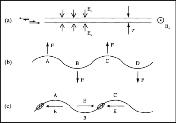
describe this mechanism. Figure 14a shows the electron sheet; Figure 14b shows the sinusoidal perturbation applied to the system; and points A and C represent electrons that are moved upward by the electrostatic force of the adjacent electrons. The electrons located at points B and D are moved downward. In Figure 14c, it can be observed that charge bunching is generated by the movement of electrons in A and C to the left and B and D to the right due to the F B force (Figure 14b). This charge bunching will increase the growth of the perturbation leading to an E B drift [2].
Figure 14: Physical mechanism of the diocotron instability.
(a) Velocity shear generated by the self-electric field of the electron
sheet, (b) Initial sinusoidal perturbation of the electron sheet, and (c)
2.6 Stability and Mode Separation
Magnetrons may have several modes of oscillation. Usually the desired operating mode in a magnetron is the π mode because it gives better stability and higher output power. In this section, different techniques for mode separation will be described. Frequency and Mode Competition
Magnetrons are comprised of many resonators coupled together. For this reason, mode competition is a common problem in magnetrons [2, 6, 58]. The mode number is defined as „n‟, and it describes the number of times the RF field pattern is repeated going around the anode once. N is defined as the number of cavities, where the maximum number for n is N/2, for mode operation. When this occurs, this mode is called the π-mode [34]. A magnetron operating in the π-π-mode has greater power output and is the most commonly used. For this reason, mode separation became very important for making magnetron oscillators reliable and efficient.
One of the most common problems in the design of magnetrons is to ensure that the operation remains in only one of the many possible resonant frequencies. It has been found that this can be achieved if the circuit is designed so that the operating resonant frequency is well separated from all other resonant frequencies of the structure [61]. Two techniques, the use of straps and the rising sun structure, are used to achieve mode
separation. These techniques will be described in the following sections. Strapping
capacitance to the resonator circuit of each cavity, and therefore it could also add some undesired modes. However, the strapping technique is designed to separate and isolate the π-mode frequency; therefore, other frequencies that could be generated are not significant in comparison to the π-mode. This way the device will not operate in other modes. Strapping was one of the first techniques used in magnetron design and was first implemented by Randall and Boot in 1941 in the cavity magnetron [7]. Figure 16shows a picture of a strapped magnetron. The wire straps are visible in the image.
Figure 15: Strapping technique. Alternate anode segments at same potential.
Figure 16: Wire strapping system of an S band cavity magnetron [58].
Rising Sun Geometry
The magnetron design for this work is the rising sun magnetron [61-63]. This design was developed in the search for a stable magnetron operation at wave-lengths close to 1 cm. This design can also achieve stability and can operate in the π-mode without strapping [1, 61-63].
The rising sun anode structure was developed by Millman and Nordsieck [61] in 1944. This design utilizes two different resonator sizes arranged symmetrically around the cathode-anode space, with resonators alternately larger and smaller (See Figure 17). The rising structure has a design that allows mode separation. By examining the field patterns that are associated with different modes, it can be observed that modes that range in the low frequencies are control by the larger cavities. On the other hand, modes
associated with higher frequencies are control by the shorter cavities. Hence, the π-mode frequency range can be found in between the resonant frequencies of the two cavities [34, 61]. Figure 17 shows a comparison of the strapped structure versus the rising sun
structure.
The rising sun magnetron is an easier geometry to handle in terms of modeling and calculations, since the technique of strapping requires a more complex model, and the calculations that could be done in two-dimension modeling are very limited. The rising sun geometry allows modeling of the magnetron in two dimensions and, therefore, greatly reduces computation time. Figure 18 shows a picture of a sixteen-cavity rising sun magnetron.
Figure 18: Sixteen-cavity rising sun magnetron from Ostron Technologies [64].
2.7 Phase Locking of Magnetrons
Phase locking of magnetrons is a technique used to control the magnetron
equivalent to that of a single relativistic magnetron, which is an expensive device, then phase locking could be used to substitute for this expensive device [25]. Phase locking has been studied since World War II with the works of Adler [66] and David [67]. They developed theories applied to phase locking of magnetrons driven by an external source, which was performed by power injection at levels significantly below the magnetron‟s output power [25]. The condition for locking is known as Adler‟s condition and is written as [66]
D 2 D o
O o
P Q P
(2.17)
where PD is the magnitude of injected power, PO is the oscillator‟s output power, D is the frequency of the injected signal, o is the free running oscillators output frequency, and Q is the quality factor of the oscillator. The work presented in this dissertation will not cover phase control of multiple magnetrons, which is a technique broadly covered in the literature [2, 25-28, 47, 65, 68]; it will focus on the phase control of oscillations of one magnetron device by using modulated, addressable, controlled electron sources.
2.8 State of the Art and New Magnetron Concept
an azimuthally modulated magnetic field, which led to modulation of the electrons over the solid cathode surface. The group is currently studying two new magnetron concepts: the inverted magnetron and the recirculating planar magnetron [3, 14, 15]. The inverted magnetron [15], as its name implies, consists of having the cathode on the outside and the anode on the inside. The main characteristics of this device are its larger cathode area, the reduction of electron end loss, and a faster startup in comparison with the conventional magnetron. These characteristics are also incorporated in the recirculating planar
magnetron. The recirculating planar magnetron [14] is considered a new class of crossed-field device that features both large area cathode and anode, meaning high current and improved thermal management. This device was designed with 12 cavities, 2 planar oscillators with 6 cavities each, operating at a frequency of 1 GHz. Mode control is still under study with this device; using the PIC code MAGIC, they have simulated phase locking, achieving an increase in mode separation and a reduction in the startup time of oscillations.
operation, since it does not allow a rapid turn ON/OFF time of the current source. Therefore, it would not allow the temporal modulation of the current sources.
The Air Force Research Lab (AFRL) developed a method to replace thermionic cathodes with explosive field-emission cathodes [51, 72]. The explosive field emission cathodes are lightweight; they deliver high currents and do not require heat for their operation. Three different types of cathodes were tested, each of them with slightly different geometries. Although, these cathodes are not as developed as thermionic cathodes, the results demonstrated that this technique provided a lower turn-on DC electric field and a uniform emission. Moreover, the use of gated field emitters has also been implemented to replace the conventional thermionic cathode. One of the few applications of gated field emitters in MVEDs has been implemented in traveling wave tubes (TWTs) [73, 74]. This project successfully demonstrated the use of modulated gated emitters in TWTs. The emitters cathode pulse time was reduced from the scale of seconds (thermionic cathode) to the scale of nanoseconds (gated emitters). It was demonstrated that the use of gated emitters has the potential to improve TWTs performance that is not achievable with conventional thermionic cathodes.
The proposed magnetron concept for this research is based on using gated field emitters placed in a shielded structure housed within the cathode to prevent ion
The front of each facet is a conductor, which forms the sole electrode. Here, the sole electrode indicates a non-emitting cathode structure. While this image shows a few large slits, the actual device concept would have hundreds of slits per facet plate with many thousands of gated emitters placed below the facet. The idea behind this concept is that the gated field emitters could be used to control the electron injection into the interaction space of the magnetron by varying the emission current both spatially and temporally. Hence, the cathode can be modulated to control the beam wave interaction and the device phase. This modulated, addressable-cathode based magnetron is actually an amplifier but is based on the cavity magnetron structure. Such a device can reduce start up times and allow phase locking with other similar devices for increased power output [26, 28, 47].
Figure 19: Proposed ten-cavity rising sun magnetron with a five-sided
faceted cathode. Each plate would have hundreds of slits with gated emitters beneath.
Anode Cathode
CHAPTER THREE:LORENTZ2E SIMULATION
3.1 Overview
This chapter describes the simulation setup, procedures, and techniques implemented in the simulation with Lorentz2E. In this research, Lorentz2E is used to study the electron trajectories in the rising sun magnetron model as well as to determine the sensitivity of the electron injection into the device from changes in the operating parameters and geometry.
3.2 Software
The Lorentz2E simulation used in this research is a 2-D serial (it uses one processor core) particle trajectory simulation code developed by Integrated Software [21]. The simulation can include both space-charge and surface-charge effects. The simulation solves for the electric fields using the Boundary Element Method (BEM) [21] and uses a 4th order Runge-Kutta technique [21] for the electron trajectory tracking. The Boundary Element Method (BEM) solves field problems by solving an equivalent source problem. In the case of electric fields, it solves for equivalent charge; while in the case of magnetic fields, it solves for equivalent currents. BEM also uses an integral formulation of Maxwell‟s Equations, which allows for very accurate field calculations [21].
In Lorentz2E, the simulation can be set to inject a fixed current with a
tool in Lorentz2E, which allows the user to change parameters such as dimensions and materials. The objective of the parametric study is to find the adequate set of parameters that will provide the optimal performance of the device: in other words, to find the optimal conditions regarding geometry and operating parameters that will guarantee the maximum number of electron rays exit the slits in the cathode plate.
3.3 Simulation Setup and Procedures
Figure 20: (a) Shielded cathode slit. Showing the stacked lateral field emission tips on each side of the slit, a pusher electrode, the sole electrode (cathode plate), and the electron trajectories. (b) Faceted cathode showing slits [12].
Figure 21: Lorentz2E model of the shielded cathode slit structure. (a) The emitters on each side, a field emission gate transparent to electrons, a pusher electrode, the sole electrode, the electrode voltages, and the dimensions; and, (b) the electron ray trajectories[12].
The structure is comprised of the following.
Field emitters:They are the source of electron rays. They were modeled as a line with a fixed injection current. The field emitters are on each side of the slit.
Slits
Cathode Cathode Plate
(a) (b)
Gate: The gate was modeled as a block that allows electron transit. The gate is biased positive with respect to the emitters to create a large electric field capable of generating field emission.
Sole electrode: Sets the interaction space electric field in the magnetron. This sole electrode is biased negative relative to the anode.
Pusher electrode: The pusher electrode is placed below the level of the field emitter. As the rays move into the slit region, the field from the pusher electrode directs the electrons up through the slit. In order to do this, the pusher electrode is biased negative relative to the sole electrode.
Collectors: Boundaries that collect particles upon collision. In the simulation, a collector is used to estimate the amount of rays that exit the slit.
Figure 22: Magnetron model used in Lorentz2E. Five-sided cathode with a smooth dummy anode showing electron ray traces from a single shielded slit structure on the left hand side of the top facet.
The sole electrode (see Figure 21) is set to -22.2 kV, and there is an axial
magnetic field of 900 G. The gate was modeled as a block that allows electron transit. All other electrodes were defined as collectors. The slit exit is 8 µm across; the sole electrode is 2 µm thick. Also shown in Figure 21 are the voltages for the electrodes and the
emitters with the sole electrode biased at -22.2 kV, the emitters biased at -22.3 kV, the pusher at -22.3 kV, and the gate at -21.7 kV. These values are obtained from this simulation for the best extraction of the electrons out of the slit [12].
3.4 Electron Trajectory Analysis
One concern for the proper operation (best extraction of the electrons out of the slit) of the magnetron is the effect of the initial electron energy distribution given the slit structure and facets. To study this effect, the electron energy distribution was determined from the simulation by developing histogram plots. The values were taken at the exit of the slit where a “collector” was placed in the simulation (see Figure 21). This analysis
included variation in the number of rays to check consistency. The simulations were divided into three cases: 50 rays (25 rays each side), 100 rays (50 rays each side), and 200 rays (100 rays each side). The energy is divided into transverse (parallel to the slit opening) and vertical (perpendicular to the slit opening). The most significant results from these simulations can be found in Chapter 4.
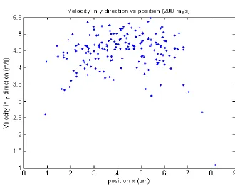
The electron velocity spreads were also extracted from the simulation. They were taken at the slit exits; the velocity was extracted from the simulation in terms of a scatter plot. The results of the electron velocity were taken in the „x‟ (horizontal) and „y‟ (vertical) direction versus position. These plots were generated for 200 rays (100 rays each side). There results can also be found in Chapter 4.
3.5 Sensitivity Simulations
One of the simulation efforts involved studying the sensitivity of the electron injection into the device with the variation in the operating voltages of the emitter and pusher electrodes as well as the location of the pusher electrode below the emitter. This study was performed to find the best conditions that would guarantee the maximum number of rays exit the slit. These tests are important for design considerations. It is useful to know the sensitivity of the field emitters in terms of voltage and location parameters. Since all of the field emitters will not operate at the same voltage, this technique is used to study a range of voltages (ΔV) that still guarantees adequate
operation. Similarly, this range can also be studied by changing the location of the pusher electrode.
was calculated. All of the simulations were completed for a total of 200 rays (100 rays each side).
In order to analyze the sensitivity of the device, a number of tests were simulated: (a) varying pusher electrode voltage, (b) varying emitter voltage, and (c) varying the geometry of the pusher electrode. The simulations were then performed by varying one major parameter while holding others constant, then changing a second parameter while varying the first. For example, the pusher electrode voltage is fixed while the emitter voltage is varied; then the pusher voltage is changed, and the emitter voltage is again varied over the same range as before. This variation can be performed within Lorentz2E using the “parametric function.” Example results of this set of simulations are presented in Chapter 4.
Table 3.1 summarizes the sensitivity simulation varied parameters.
Table 3.1: Lorentz2E Magnetron Model Sensitivity Simulations.
Major Parameter Value of Major Parameter
Varied Parameter
Values of Varied Parameter
Pusher Voltage -22.20 kV to -22.37 kV Emitter Voltage -22.20 kV to -25.0 kV Emitter Voltage -22.20 kV to -22.37 kV Pusher Voltage -22.20 kV to -25.0 kV Pusher Geometry 1.70 um thick Emitter Voltage -22.20 kV to -25.0 kV
Pusher Voltage -22.20 kV to -22.37 kV
Pusher Geometry 1.70 um thick Pusher Voltage -22.20 kV to -25.0 kV Emitter Voltage -22.20 kV to -22.37 kV
Pusher Geometry 0.4475 um thick Emitter Voltage -22.20 kV to -25.0 kV Pusher Voltage -22.20 kV to -22.37 kV
CHAPTER FOUR: LORENTZ2E SIMULATION RESULTS
4.1 Overview
This chapter presents the simulation results completed with the particle trajectory simulation code Lorentz2E. These simulations include energy distribution analysis, electron velocity analysis, and the sensitivity analysis. This study was completed to use as a reference for future work in the fabrication of the actual magnetron device with gated vacuum field emitter arrays placed in a shielded structure (slits). As was discussed in the previous chapter, the slits are used to protect the emitters from the harsh environment of the magnetron interaction space including ion back bombardment.
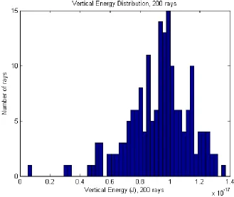
4.2 Energy Distribution Analysis
The energy distribution analysis was completed by developing histogram plots of the energy in the transverse direction (parallel to the slit opening) and the vertical
use of 200 rays appears to be needed to get a well-defined distribution. The distribution energy plots were studied to find the best consistency and to see how many electron rays were needed to form a well-defined electron hub around the cathode. As shown in the results, 200 rays provided a consistent distribution.
Figure 24: Vertical energy distribution from Lorentz2E for 200 electron rays.
4.3 Electron Velocity
In order to look at the velocity spread at the slit exits, the velocity was also extracted from the simulation in terms of a scatter plot. The previous simulation
Such velocity plots could be used in future magnetron simulations for studying the effects of velocity spread on the device performance.
Figure 25: Velocity in the x-direction versus position for 200 electron rays.
4.4 Sensitivity Simulations
All the results shown in this section are for simulations using a total of 200 electron rays (100 rays per side). The Lorentz2E simulation can be run to include the space-charge effects of the individual rays on adjacent rays; however, the simulation will not allow both the ray charge and the simulated space-charge hub at the same time. Therefore, the results shown here do not include ray space charge simultaneously with the hub charge. However, simulations with the ray space charge and no hub charge have been run in previous work [12] and do not show significant effects on the ray trajectories at the slit exits at the current densities simulated. The electron density in the magnetron was found from previous work [12] simulations to have a peak value of 6x1010 cm−3. The total charge in the volume was estimated to be −1.35x10⁻⁸ C. To be conservative, a total volume charge of −1.5x10⁻⁸ C was then used in the simulation to represent the charge hub [12]. The sensitivity simulations are summarized in Table 3.1 from Chapter 3. The results are summarized in three parts: (a) variation of the pusher electrode voltage, (b) variation of the emitter voltage, and (c) variation of the geometry (dimensions) of the pusher electrode.
(a) Varying Pusher Electrode Voltage
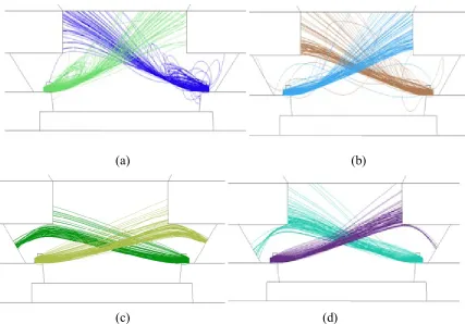
As can be seen, the rays begin to strike the sole electrode walls and be lost or are turned back to the cathode depending upon the voltage. The simulations were repeated for four additional pusher electrode voltages. These results are presented in Appendix A.
(a) (b)
(c) (d)
Figure 27: Pusher Electrode Voltage at -22.20 kV. Emitter Voltage at (a) -22.20kV, (b) -22.26 kV, (c) -22.34 kV, and (d) -22.5 kV.
Collector Current Analysis
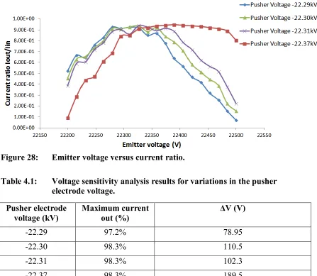
between 10-20 rays in total. This amount of emitter current loss (injected emitter current) was calculated and subtracted from the original injected emitter current. The voltage sensitivity (ΔV) was calculated for this threshold value. These results are shown in Table 4.1. This means that the resulting ΔV calculated for each pusher electrode value shows the sensitivity of the emitters to the change in parameters. A large ΔV indicates low sensitivity to voltage variation, which is desirable for device operation. In this set of simulations, the best case indicates a pusher electrode of -22.37 kV with a ΔV of 189.5 V.
Figure 28: Emitter voltage versus current ratio.
Table 4.1: Voltage sensitivity analysis results for variations in the pusher electrode voltage.
Pusher electrode voltage (kV)
Maximum current out (%)
ΔV (V)
-22.29 97.2% 78.95
-22.30 98.3% 110.5
-22.31 98.3% 102.3
(b) Varying Emitter Voltage
The emitter voltage was set as a major parameter with the pusher electrode
voltage varied by the parametric function. The emitter voltage was varied from -22.20 kV to -22.37 kV in six cases, including the standard case [12]. The pusher electrode voltage was varied from -22.20 kV to -25.0 kV using 20 steps. Figure 29 show the results of the ray trajectories at different pusher electrode voltages with a fixed emitter voltage of -22.20 kV. As seen in Figure 29, as the pusher voltage increases (pusher voltage > -22.34 kV), the electron trajectories are turned back, and they never hit the collector plate. Therefore, no rays will exit the slit.
(a) (b)
(c) (d)
Collector Current Analysis
A diagnostic was placed at the collector to measure the number of rays that will hit the collector. In Figure 30, a plot of the pusher electrode voltage vs. the rate of Iout/Iin at different emitter voltages is presented. The voltage sensitivity (ΔV) was calculated and the best case results are presented in Table 4.2. In this case, the best case corresponds to the emitter voltage of -22.37 kV with a ΔV = 157.9. This case also guarantees 98% of the rays exit the slit.
Figure 30: Pusher electrode voltage vs. current ratio.
Table 4.2: Voltage sensitivity analysis results for variations in the emitter voltage.
Emitter voltage
(kV) Maximum current out (%) ΔV (V)
-22.26 91.1% 63.15
-22.29 97.2% 78.95
-22.30 97.8% 94.74
-22.31 97.2% 126.3
(c) Varying the Geometry
In this section, the simulation results are from the variation of the geometry of the pusher electrode; the simulations shown in Section (a) and (b) were repeated for each geometry. The pusher electrode has a thickness of 0.9795 µm from the reference model studied in [12]. This thickness was modified to its maximum and minimum to study the device sensitivity due to changing the geometry/dimensions. The simulations are
performed for two different pusher electrode thicknesses: geometry (1) corresponds to a thickness of 1.70 µm and geometry (2) corresponds to a thickness of 0.4475 µm. Some examples of these results are presented in this section. The rest of the results are presented in Appendix A. Figure 31 and Figure 33 correspond to results using a pusher electrode thickness of 1.70 µm with a fixed pusher electrode voltage and a fixed emitter voltage, respectively. Figure 35 and Figure 37 correspond to the results of using a pusher electrode thickness of 0.4475 µm with a fixed pusher electrode voltage and a fixed
(a) (b)
(c) (d)
Figure 31: Pusher Electrode Voltage at -22.20 kV. Emitter Voltage at (a) -22.20 kV, (b) -22.26 kV, (c) -22.34 kV, and (d) -22.5 kV. Pusher Electrode Thickness of 1.70 µm.
Collector Current Analysis with Pusher Electrode Voltage Constant and Varying Emitter Voltage for Pusher Electrode Thickness of 1.70 µm
![Figure 2: Microwave oven [6].](https://thumb-us.123doks.com/thumbv2/123dok_us/8922042.1842476/22.612.139.512.140.342/figure-microwave-oven.webp)

![Figure 9: Various forms of the anode block in a magnetron: (a) Slot type, (b) Vane type, (c) Rising sun, and (d) Hole-and-Slot type [57]](https://thumb-us.123doks.com/thumbv2/123dok_us/8922042.1842476/33.612.279.408.129.255/figure-various-magnetron-slot-vane-rising-hole-slot.webp)
![Figure 10: Equivalent circuit of an eight-cavity magnetron [1].](https://thumb-us.123doks.com/thumbv2/123dok_us/8922042.1842476/34.612.238.412.73.244/figure-equivalent-circuit-cavity-magnetron.webp)