DIGITAL facility, Marlboro, Massachusetts
CORPORATE PROFILE
Digital Equipment Corporation designs. manufactures, sells and ser-vices computers and associated peripheral equipment, and related software and supplies. The Company's products are used world-wide
· microcomputer
inter~aces
handbook
Copyrlght© 1981 Digital Equipment Corporation. All Rights Reserved.
Digital Equipment Corporation makes no rep'resentation that the In-terconnection of its products in the manner described herein will not infringe on existing or future patent rights, nor do the descriptions contained herein imply the granting of license to make, use, or sell equipment constructed in accordance with this description.
The information in this document is subject to change without notice and should not be construed as a commitment by Digital Equipment Corporation. Digital Equipment Corporation assumes no responsibili-ty for any errors that may appear In this manual.
DEC, DECnet, DECsystem-10, DECSYSTEM-20, DECtape, DECUS, DECwriter, DIBOL, Digital logo, lAs, MASSBUS, OMNIBUS,
PDP, PDT, RSTS, RSX, SBI, UNIBUS, VAX, VMS, VT are trademarks of
Digital Equipment Corporation
This handbook was designed, produced, and typeset by DIGITAL's New Products Marketing using an In-house text-processing system
CONTENTS
PART 1 INTRODUCTION
GENERAL ... 1
LSI-11 FAMILY CHARACTERISTICS ... 1
SPECiFiCATIONS ... 4
DESCRIPTION OF OPTION CATEGORIES ... 5
CONFIGURATION ...•... 25
PART 2 LSI-11 BUS INTERFACE DESCRIPTIONS AAV11-A 4-Channel 12-Bit D/ A Converter ... 33
ADV11-A Analog to Digital Converter ... 45
BA 11-M Expansion Box ... 67
BA11-N Mounting Box ... 74
BA11-VA Expansion Mounting Box ... 83
BDV11 Diagnostic, Bootstrap, Terminator ... 86
DCK11-AA, -AC Program Transfer Interface ... 114
DCK11-AB, AD Direct Memory Access Interface ... 134
DDV11-B Backplane ... 159
DLV11 Serial Line Unit. ... 165
DLV11-E Asynchronous Line Interface ... 180
DLV11-F Asynchronous Line Interface ... 201
DLV11-J Four Asynchronous Serial Interfaces ... 221
DLV11-KA EIA to 20 mA Converter ... 251
DRV11 Parallel Line Unit ... 261
DRV11-B Direct Memory Access Interface ... 282
DRV11-J High-Density Parallel Interface ... 306
DRV11-P LSI-11 Bus Foundation Module ... 310
DUV11 Line Interface ... 335
DZV11 Asynchronous Multiplexer ... 357
H780 Power Supply ... ' ... 385
H909C General Purpose Logic Enclosure ... 420
H984 Series Cabinets ... 422
H9270 Backplane ... 425
H9273-A Backplane ... 431
H9281 Backplane ... 435
H9800-A Cabinet ... 441
IBV11-A Instrument Bus Interface ... 443
KPV11-A,-B,-C Power-Fail/Line-Time Clock/Terminator ... 465
KWV11-A Programmable Real-Time Clock ... 488
LAV11 Printer Option ... 510
REV11-A Terminator, REV11-C DMA Refresh, Bootstrap ... 538
RKV11-D RK05 Disk Drive Controller ... 547
RLV11 RL01 Disk Drive Controller ... 563
RXV11 Floppy Disk Option ... 592
RXV21 Floppy Disk Option ... 608
TEV11 Terminator ... 629
TU58 Cartridge Tape Drive ... 630
VK170-CA Serial Video Module ... 669
W9500 Series High-Density Wire-Wrappable Modules ... 685
APPENDIX A ASSIGNMENT OF ADDRESSES AND VECTORS··· ... · .... 690
APPENDIX B LSI-11 BUS SIGNALS .. ... 708
APPENDIX C NOMENCLATURE FOR CIRCUIT SCHEMATICS ···719
APPENDIX D ASYNCHRONOUS SERIAL LINE UNIT (SLU) COMPARISONS ... 721
APPENDIX E COMPARISON OF DATA TRANSMISSION TECHNIQUES ... 729
APPENDIX F INTEGRATED CIRCUITS ... 732
INTRODUCTION
GENERAL
This handbook is a reference guide for the interface and peripheral hardware options that can be installed on the LSI-11 bus. It includes descriptions, specifications, configuration information, programming information as applicable to the options, and functional theory. Be-cause the hardware options described in this handbook are designed to interface with a processor via the LSI-11 bus, the user should be familiar with the contents of the appropriate processor handbook. The handbook is organized into two parts. Part '1 contains general information about microcomputer interfaces; Part 2 contains descrip-tion of the interface opdescrip-tions in alphanumeric sequence.
Digital Equipment Corporation designs and manufactures the options described in this handbook. The general design criterion was to pro-vide maximum system throughput for options when installed on the LSI-l1 bus. LSI-11 bus-compatible processors, interfaces, and peri-pherals are designed to work together, providing a broad spectrum of system-compatible hardware options. The memory and peripheral devices can be used with various LSI-11 bus configuration; the system can later be expanded or modified to meet new system requirements. This hardware flexibility, when coupled with DIGITAL software and support, provides a single source for all present and future microcom-puter processing needs.
LSI-11 FAMILY CHARACTERISTICS
LSI-11 bus systems include various processors, memory and peri-pheral device options, and software. Some of the characteristics of the LSI-11 bus systems are:
• Low-cost powerful components for integration into any small- or medium-sized computer system.
• Direct addreSSing of all memory locations ·and peripheral device registers.
• Efficient processing ·of a-bit bytes (characters) without the need to rotate, swap, or mask.
• Asynchronous bus operation that allows system components to run at their highest possible speed; replacement with faster devices means faster operation without other hardware or software changes.
INTRODUCTION
• Inherent direct "memory access capabilities for high data rate de-vices.
• A bus structure that provides position-dependent priority for peri-pheral device interfaces connected to the 1/0 bus.
• Vectored interrupts that allow service routine entry without device polling.
Processors
The processor is connected to the LSI-11 bus (backplane) as a sub-system that executes programs and arbitrates usage of the LSI-11 bus for peripherals. It contains multiple, high-speed, general-purpose reg-isters that can be used as accumulators, address pointers, index registers, and other specialized functions. The processor can perform data transfers directly between peripheral input/output (1/0) devices and memory without disturbing the processor registers. Data transfers include both 16-bit word and 8-bit byte data.
LSI-11 Bus
System components, including the processor, memory, and peripher-als, are interconnected and communicate with each other via the LSI-11 bus. The form of communication is the same for all devices on the bus; instructions that communicate with memory can communicate with peripheral devices. Each device, including memory locations and peripheral device registers, is assigned an Individual byte or word address on the LSI-11 bus.
The LSI-11 bus supports 18-bit addresses. However, processors and peripherals having a 16-bit addressing capability are completely PDP-11 hardware- and software-compatible within the 16-blt limitation. By PDP-11 convention, all peripheral device addresses are located within the upper 4K address space in the system, whether 16-blt or 18-blt addresses are used. This 4K address space is called the I/O page or "bank 7."
Whenever the I/O page is addressed, the processor must assert the BBS7 L bus Signal. All peripheral devices use this signal line during addressing rather than decoding address bits <15:13> or <17:13>. An active (asserted) BBS7 L Signal will always indicate an address in the I/O page, enabling peripheral device addressing.
INTRODUCTION
control in exactly the same manner as memory locations. Unique ad-dresses within the 110 page are encoded on address bits <12 :00>.
NOTE
Address bits, for the purpose of this discussion, are logical states present on LSI-11 bus signal lines BOAL <17:00> L during the addressing portion of a bus cycle.
Refer to the appropriate processor handbook for a complete descrip-tion of bus transacdescrip-tions, Including bus cycles, addressing, etc. Device Registers
All peripheral devices are defined by one or more device registers that are addressed as part of the main memory. These registers are gener-ally designated control and status registers.
Control and status registers (CSRs) contain all the necessary Informa-tion to establish communicaInforma-tions with the device. Some devices will require fewer than 16 status bits, while other devices could require more than 16 bits and therefore will require additional registers. The bits of the CSR have predetermined assigned functions. Typical bit functions include Interrupt enable, error, done or ready, and enabled. Data buffer registers (OBRs) are for temporarily storing data to be transferred Into and out of the processor. The number and type of data registers is a function of the Individual peripheral device require-ments.
Interrupts
INTRODUCTION
device. Once the device service routine execution has been complet-ed, control is returned either to the previously Interrupted program or to another peripheral device requesting Interrupt service.
Memory Address
Memory addresses are generally limited to the address space other than the I/O page. However, the I/O page can contain read-only memory (ROM) for disk bootstraps, paper tape loaders, diagnostics, etc. or read/write memory for DMA buffers. The system designer must use care in assigning memory addresses within the I/O page to avoid conflicts with peripheral device addresses used for actual system hardware, or addresses that system software may attempt to access for peripheral devices not actually Installed In the system. See Appen-dix A for the standard assignments of the addresses In the I/O page. SPECIFICATIONS
All the LSI-11 bus modules will operate under the following conditions: Temperature
Humidity
50 to 600 C (410 to 1400 F)
10 to 95% (no condensation) When operating at the maximum outlet temperature (600
Cor 1400 F).
adequate air flow must be maintained to control the Inlet to outlet temperature rise across the modules to 5 0 C (90 F) maximum. The air
flow should be directed to flow across the modules.
All the Individual module specifications are Included In the detailed descriptions of the peripheral or option. A summary of the module characteristics Is provided In Table 2; these characteristics are de-fined as follows:
1. The option designation Is the alphanumerical code assigned to the option.
2. The module number Is the number assigned to the Interface mod-ules that are connected to the LSI-11 bus. This number Is printed on the module handle and can be used as a quick reference to determine what specific options are Installed In any system. The module numbers are listed numerically In Table 3 so that the ~ser can identify the options Installed by using the module numbers. 3. The module description Identifies the category of the option. 4. The power requirements specify the power by the option when
INTRODUCTION
5. The bus loads for ac and dc loading are provided so that the user can calculate the total ac and dc loading for any system.
6. The Interface modules are standarlzed as either a double or a quad and all are extended length. The double size module is 13.2 cm (5.2 in.) high, 22.8 cm (8.9 in.) long, and 1.27 cm (0.5 In.) wide. The quad size module is 26.5 cm (10.5 In.) hi'gh, 22.8 cm (8.9 in.) long, and 1.27 cm (0.5 in.) wide (Figure 1).
DESCRIPTION OF OPTION CATEGORIES
The LSI-11 bus peripherals and options are classified into general categories that pertain to their performance and function. This listing Indicates the wide span of equipment capability available to the user
Interface Options
AAV11-A The AAV11-A Is a 4-channel, 12-bit dlgital-to-analog converter module that Includes control and interfac-ing circuits. It has four 01 A converters, a dc-dc converter that provides power to the analog circuits, and a precision voltage reference. Each channel has its own holding register that can be addressed sepa-rately and provides 12 bits of resolution. Bits 0, 1, 2, and 3 of the fourth holding register are brought out to the 110 connector so that they can be used as a 4-bit digital output register.
ADV11-A The ADV11-A Is a 12-bit successive approximation analog-to-digital converter that samples analog data at specified rates and stores the digital equivalent value for processing. The multiplexer can accommo-date up to 16 single-ended or 8 quasi-differential inputs. The converter uses a patented auto-zeroing design that measures the sampled data with respect to its own offset and therefore cancels out its own offset error.
DRV11
DRV11-B
DRV11-J
DRV11-P
INTRODUCTION
The DRV11 Is a parallel interface module that Is used
to interconnect the LSI-11 bus with general-purpose, parallel line TTL or DTL devices. It allows program-controlled data transfers at rates up to 40K words per second and uses LSI-11 bus Interface and con-trollogic to generate interrupts and process vector handling. The data are handled by 16 dlode-clamped input lines and 16 latched output lines. There are two 40-pin connectors on the module for user interface applications.
The DRV11-B is an interface module that uses direct memory access (DMA) to transfer data directly between the system memory and an I/O device. The interface is programmed by the processor to move variable length blocks of 8- or 16-blt data words to or from specified locations in the system memory. Once programmed, there is no processor Interven-tion required. The module can transfer up to 250K 16-bit words per second in the single-cycle mode and up to 500K 16-bit words per second in the burst mode. It also allows read-modify-restore operations. Sixty-four input/output data lines are now available on a double-height module for the LSI-11 12,
LSI-11/23, PDP-11 103, and PDP-11 123. The DRV11-J
IBV11-A
KWV11-A
INTRODUCTION
les and wire-wrap pins for Interconnecting the user's curcuits. The plated-through holes can accept 6-, 8-, 14-,18-,20-,22-,24-, and 40-pln dual-In-line -Integrated circuits or discrete components.
The IBV11-A Is an Interface module that Intercon-nects the LSI-11 bus with the instrument bus de-scribed In IEEE standard 4881975, "Digital Interface for Programmable Instrumentation." The IBV11-A makes a processor-controlled programmable in-strument system possible. The module can accom-modate up to 15 IEEE-488 devices and Is PDP-11 software-compatible.
The KWV11-A Is a programmable real-time
clock/counter that provides a means of determining time intervals or counting events. It can be used to generate interrupts to the processor at predeter-mined intervals or establish timing between Input and output events. It can also Initialize the ADV11-A analog-to-dlgltal converter by a clock counter over-flow or by firing a Schmitt trigger. The clock counter has a resolution of 16 bits and can be driven by any one of five crystal-controlled frequencies (100 Hz to 1 MHz), from a line frequency Input, or from a Schmitt trigger fired by an external Input. The mod-ule can operate In any of four programmable modes: single interval, repeated Interval, external event tim-ing, and external event timing from zero base.
Communications Options
DLV11 The DLV11 is a serial line unit (SLU) that interfaces with asynchronous serial I/O devices. The module has jumper-selectable baud rates (50-9600) and se-rial word format that includes the number of stop bits, number of data bits, and even, odd, or no parity bit. The DL V11 can support 20 rnA current loop In-terfaces or EIA "data leads only" inIn-terfaces. DLV11-E The DL V11-E is an asynchronous line interface
DLV11-F
DLV11-J
DUV11
INTRODUCTION
transfers It to the LSI-11 bus. Also, It accepts parallel data from the LSI-11 bus, converts It to serial data, and transmits It to the peripheral device. The module has jumper-selectable or software-selectable baud rates (50-19,200), and Jumper-selectable data bit formats. The DL V11-E offers full modem control for EIA/CCITT Interfaces.
The DL V11-F Is an asynchronous line Interface mod-ule that interconnects the LSI-11 bus to several types of standard serial communications lines. The mod-ule receives serial data, converts It to parallel data, and transfers It to the LSI-11 bus. It also' accepts parallel data from the LSI-11 bus, converts It to serial data, and transmits It to the peripheral device. The module has jumper-selectable or software-selecta-ble baud rates (50-19,200) and jumper-selectasoftware-selecta-ble data bits. The DL V11-F supports either 20 rnA cur-rent loop or EIA standard lines, but does not Include modem control.
The DL V11-J contains four Independent asynchro-nous serial line channels used to Interface peripheral devices to the LSI-11 bus. Each channel transmits and receives data from the peripheral device over EIA data leads (lines that do not use a control line). The module can be used with 20 mA current loop devices if a DL V11-KA adapter Is used. The DLV11-J has jumper-selectable baud rates from 150 to 39.4 K baud.
The DUV11 synchronous line Interface module esta-blishes a data communication line between the LSI-11 bus and a Bell 201 synchronous modem or equi-valent. The module is fully programmable with . respect to sync characters, character length (to to 8
OZV11
INTRODUCTION
The OZV11 is an asynchronous mu1tiplexer interface module that interconnects the LSI-11 bus with up to four asynchronous serial data communications channels. The module provides EIA interface voltage levels and data set control to permit dial-up (auto-answer) options with full-duplex modems such as Bell models 103, 113, 212, or equivalent. The DZV11 does not support half-duplex operations or the se-condary transmit and receive operations available In some modems such as Bell 202. The OZV11 has ap-plications in data concentration and collection sys-tems where front-end syssys-tems interface to a host computer and for use in a cluster controller for ter-minal applications.
Expansion Memories (For detailed memory descriptions, see the Microcomputer Processor Handbook)
MMV11-A The MMV11-A is a 4K
x
16-bit core memory option that provides nonvolatile read/write storage. The memory can be configured by bank addressing switches. The module is limited to LSI-11 bus back-planes that contain the LSI-11 bus In both the A/B bus and the C/O slots.MRV11-AA
MRV11-BA
MRV11-C
The MRV11-AA is a read-only memory module on which the user can install fusible link, program-mable, read-only memory (PROM) chips or masked read-only memory (ROM) chips. The user selects the address space of the memory by configuring remov-able jumper wires.
The MRV11-BA is a read-only memory module that uses ultraviolet (UV) erasable, programmable, read-only memory (EPROM) integrated circuits. The mod-ule also contains a 256
x
16-bit random access memory (RAM) that can be used as a "scratchpad" or "stack" by the system. software.MSV11-B
MSV11-CD
MSV11-D,-E
MXV11-A
INTRODUCTION
PROMs. It accepts several densities of ROM chips up to and including 4K X 8 chips. Using these high-density chips gives the module a total capacity of 64K bytes. The contents of the module can be ac-cessed in one of two ways-either directly or win-dow-mapped. Direct access provides total random access to a" ROM locations on the module. Window-mapping provides two 2K-byte windows in memory address space to access 2K-byte segments of the ROM array. The segments that are viewed through each window can be varied under program control. The MSV11-B is a 4K
x
16-bit dynamic MaS read/write memory module. The user can select the memory addresses of the module by configuring re-movable jumpers. The memory refresh must be con-trolled by external bus signals.The MSV11-CD is a 16K X 16-bit dynamic MaS read/write memory module. Refresh Is automatically performed by the module but It can be disabled if the user wishes to use the LSI-11 bus refresh signals. This memory module can be configured to operate in the battery backup mode. The user can configure the memory addresses by selecting switch settings. The MSV11-D module has either 8K, 16K, or 32K X
16 bits of MaS memory. The MSV11-E Is the same as the MSV11-D except that It has an 18-bit word that generates and detects byte parity for each word. The modules have an on-board memory refresh and perform the necessary LSI-11 bus cycles. The mem-ory addressing is selectable by the user by configur-ing switch settconfigur-ings. The module can use a battery backup system to preserve data when primary power is lost.
Peripherals LAV11
LPV11
INTRODUCTION
provided for
+5 V
read-only memories.1
K X 8, 2Kx
8, or 4K X 8 ROMS may be used. The sockets may
also be used for 256 words of bootstrap code. The two asynchronous serial lines transmit and receive EIA-423 signal levels from 150 baud to 38.4K baud. 20 mA active or passive current loop operation at 110 baud may be obtained with the DLV11-KA EIA to 20 mA converter option. The serial lines will not sup-port the reader run function of the DL V11-KA option. The serial lines provide error Indicator bits for over-run error, frame error, and parity error, but do not have modem controls. Serial line 1 may be config-ured to respond to a break signal. The serial lines have signal level Interrupt logic and should be placed after multi-level devices on an LSI-11/23 sys-tem. Serial line 1 may be used as a console port, or, along with serial line 0, may be used with any of several standard types of serial communication de-vices. The 60 Hz clock signal can be selected by a wirewrap Jumper to provide line-time clock Inter-rupts on the bus.
The LAV11 option consists of an LA 180 DECprlnter, an interface module, and a BC11 S-25 Interface ca-ble. The interface module provides Interconnection between the LA 180 DECprlnter and the LSI-11 bus. The module outputs ASCII characters to the printer and monitors various printer operations that require operator control.
RKV11-0
RLV11
RXV11
RXV21
INTRODUCTION
The RKV11-0 option consists of an RK05 disk drive controller, an LSI-11 bus Interface module, and an RK05J disk drive. The RK05 disk drive controHer can be used with up to eight RK05J disk drive units to form a mass memory storage system that contains up to 21 M bytes of storage. The RKV11-D system Is block-oriented but is capable of transferring from 1 to 218 consecutive data words without reinitiation or
processor Intervention. The data transfers occur from the RKV11-D to the system memory by direct memory access (DMA) and operate at maximum bus bandwidth. The system can use either RK05J or RK05F disk drives and the controller can be mount-ed In a standard 48.3 cm (19 In.) cabinet.
The RLV11 option interfaces the LSI-11 bus with an RL01 disk drive controller and an RL01 disk drive assembly. The controller can only be used In an H9273-A type backplane which Incorporates an LSI-11 bus in slots A and B, with an Interboard bus In slots C and D. The controller can Interface up to four RL01 disk drives for a complete system of 21
M
bytes of storage. The RL01 disk drive Is a random access, mass storage system that stores data in fixed length blocks on a preformatted disk cartridge. Each drive can store up to 5.24 million bytes and the complete system can store u~ 21 million bytes. The RLV11 transfers data using direct memory access (DMA) techniques; this allows data t.r~nsfers without proc-essor Intervention and at busjbandwldth speed. The RXV11 option consists of an interface module, cable assembly, and either a single or dual drive RX01 floppy disk. This option is a random access mass storage device that stores data in fixed-length blocks on a preformatted flexible diskette. Each diskette can store and retrieve up to 256K, 8-bit bytes of data. The RXV11 system Is rack mountable in the standard 48.3 cm (19 In.) cabinet.TU58
VK170-CA
INTRODUCTION
diskette can store and retrieve up to 512K 8-bit bytes of data. The RXV21 system is rack-mountable and consists of an Interface module, an interface cable, and either a single or dual RX02 floppy disk drive. The interface module converts the RX02 1/0 bus to the LSI-11 bus structure. It controls the RX02 inter-rupts to the processor, decodes device addresses for register selection, and handles the data inter-change between the RX02 and the processor via DMA transfers. Power for the Interface module is supplied by the LSI-11 bus.
The TU58 Is a low-cost intelligent mass memory de-vice that offers random access to block-formatted data on pocket-size cartridge media. It is Ideal as a small computer systems device, as inexpensive ar-chive mass storage, or as a software update distribu-tion medium. A dual drive TU58 offers 512 Kb of storage space, making it one of the lowest cost com-plete mass storage su bsystems available. For mounting flexibility, the TU58 Is offered both as a component level subsystem and as a fully powered 5%" rack-mount subsystem.
INTRODUCTION
Backplanes
The four backplane options available for the LSI-11 bus are presented in the following paragraphs.
H9270 A 4 X 4 (four rows of four slots each) backplane with card guide assembly. LSI-11 bus in rows A-B and C-D. Accepts 8 double-height modules or 4 quad-height modules or combinations of both.
H9273-A A 9 X 4 (nine rows of four slots each) backplane with card guide assembly. LSI-11 bus in rows A-B only. Special interconnect bus in rows C-D.A ccepts dou-ble-height or quad-height modules.
H9281
DDV11-B
Enclosures
H909-C
BA11-M
BA11-N
A 2-slot backplane available In 4-, 8-, or 12-slot op-tions. Accepts double-height modules only. A 9 X 6 (nine rows of six slots each) backplane. LSI-11 bus in rows A-B and C-D. Rows E-F are unbussed except for +5V and ground. Accepts 18 double-height or 9 quad-double-height modules or combinations of both.
A 13.3 cm (5.25 in.) high, 48.3 cm (19 In.) wide enclo-sure which can be mounted in a 48.3 cm (19 In.) rack or as a stand-alone. Accommodates the DDV11-B backplane or a 9 X 6 system mounting unit or houses non-standard mounting arrangement. In-cludes cooling fan, cord guide, cable restraints, front bezel, and connector block.
BA11-VA
Cabinets H984-B
H9800-A
Power Supplies
INTRODUCTION
The BA 11-VA Is a small form-factor package provid-Ing mounting space and power for four LSI-11 /2 or LSI-11 /23 family modules. This package, plus the high functionality of DIGITAL's microcomputer prod-ucts, allows LSI-11 microcomputer applications to be implemented within a space smaller than that re-quired for many 8-blt systems.
A low-profile cabinet with four casters. Provides mounting space for standard 48.3 cm (19 in.) panels and enclosures In rack at front or rear. Includes dis-tribution panel (115 Vac, 230 Vac)
A low-profile system desk with casters. Provides mounting space for standard 48.3 cm (19 In.) panels and enclosures. Includes distribution panel (115 Vac, 230 Vac)
H780 Provides +5V ±4%, 18 A (max) and + 12V ± 3%, 3.5 A (max) at 110 Vac and features line-time clock, and power-fail/automatic restart. Available primary power of 115 or 230 Vac and with or without master and slave console .
. Cables and Connectors
Various preassembled cables in different lengths are available for use with interface and communications options. See Appendix C for commonly used cables. Wlre-Wrappable Modules
W9500 Series: LSI-11 Bus-Compatible Wlre-Wrappable Modules (W9511, W9512, W9514 AND W9515) - The LSI-11 bus-compatible wire-wrappable modules consist of quad-height and double-height modules. Two LSI-11 bus-compatible modules are available without DIP sockets.
W9514
W9512
W9515
INTRODUCTION
Power and ground connections are V-AA2, BA2, CA2, DA2
GND-AT1, BT1, CT1, DT1, AC2, BC2, CC2, DC2
Same as W9511 except with 58 pre-mount-ed DIP sockets.
Power and ground connections are the same as W9511
Double-height, extended-length, single-width module with Flip-Chip handle. No DIP sockets Included. One 40-pln male connec-tor premounted on board.
Power and ground connections are GND-AT1, BT1,AC2, BC2
Same as W9512 except with 25 pre-mount-ed 01 P sockets.
Power and ground connections are the same as W9512
Integrated Circuits
DCK11AA, -AC
DCK11AB, -AD
The DCK11-AA and -AC CHIPKITs provide the logic necessary for a program transfer interface to the LSI-11 bus. The DCK11-AA kit contains one DC003 Interrupt Chip, one DC004 Protocol Chip, and four DC005 Transceiver/Address Decoder/Vector Select Chips. The DCK11-AC kit contains previous chips plus one W9512 double-height, extended length, high-density wire-wrappable module and one BC07D-10 ten-foot, 40-connector plug-in cable.
The DCK11-AB and -AD CHIPKITs provide the logic necessary for a Direct Memory Access (DMA) inter-face to the LSI-11 bus. The DCK AB. The DCK 11-AB kit contains one DC003 Interrupt Chip, one . DC004 Protocol Chip, four DC005
wire-wrappa-INTRODVCTION
ble module and one BC07D-10 ten-foot, 40-connec-tor plug-in cable. DMA applications use the same chips as program control interfaces, plus two DC006s for word or byte address counters and a DC010 DMA buscontrollC.
Miscellaneous Options
BDV11 The BDV11 module has 2K words of read-only mem-ory (ROM) that contains diagnostic and bootstrap programs. These programs are user-selectable by setting dip switches. The diagnostic programs will test the processor, the memory, and the user's con-sole. The bootstrap programs can boot most LSI-11 peripheral devices. The module also has 120-ohm bus terminator circuits.
The user can add up to 16K of read-only memory (ROM) and up to 2K words of erasable program-mable ROM (EPROM) on the module. This 18K words of additional memory can be used with no Increase in the amount of 1/0 address space. KPV11-A, -B, The KPV11-A module generates power-up and -C power-down sequences, monitors for a power-fall
condition, and generates the line-time clock (LTC) function. The KPV11-B Is the same as the "A" except that it provides 120-ohm termination circuits. The KPV11-C Is the same as the "A" except that It pro-vides 220-ohm termination circuits. The module can be Installed on any backplane or remotely installed via an optional cable.
REV11-A, -C The REV11-C module has a bootstrap ROM and direct memory access (DMA) refresh circuits. The !"
REV11-A is Identical to the REV11-C except It has additional 120-ohm termination circuits.
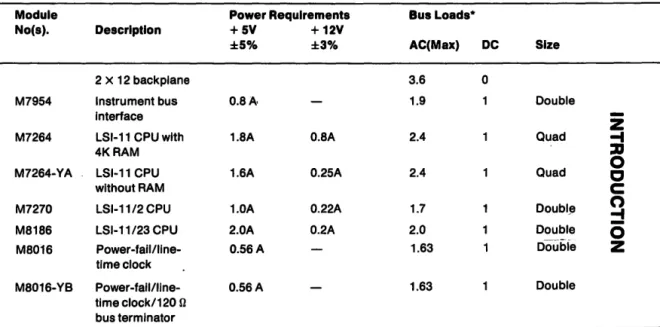
Table 1 Module Specifications
Option Module Power Requirements Bus Loads*
Deslg. No(s). Description +5V + 12V
±5% ±3% AC(Max) DC Size
AAV11-A A6001 4-channel,12-blt 1.5A 0.4A 1.9 Quad
01 A converter
ADV11-A A012 16-channel, 12-blt 2.0A 0.45 A 3.25 Quad
AID converter
Z
BDV11 MB012 Bootstrap, 1.6A 0.07 A 2.0 Quad
...
terminator,
::D
diagnostic
0
...
C
Q)
DDV11-B 6
x
9 backplane 6.4 0C
DLV11 M7940 Asynchronous serial 1.0A 0.18A 2.5 Double
n
line Interface
:::!
DLV11-E MBOH Asynchronous line 1.0 A 0.1BA 1.6 Double
0
Interface
Z
DLV11-F MB02B Asynchronous line 1.0A 0.1BA 2.2 Double
Interface
DLV11-J MB043 4 asynchronous 1.0A 0.25 A Double
serial Interfaces
-" (0
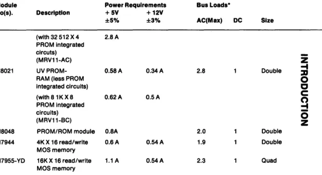
Table 1 Module Specifications
Option Module Power Requirements Bus Loads·
Oeslg. No(s). Description +5V +12V
±5% ±3% AC(Max) DC Size
DRV11 M7941 Parallel line unit 0.9A 1.4 Double
interface
DRV11-8 M7950 DMA Interface 1.9A 3.3 Quad
Z
....
DRV11-J M8049 64-lIne parallel 1/0 1.6A 1.8A 2.0 Double
::D
DRV11-P M7948 Foundation 1.0A 2.1 Quad
0
module + user logic C C
DUV11 M7951 Synchronous serial 0.86 A 0.32 1.00 Quad
,n
line interface
:!
DZV11 M7957 Asynchronous 1.15A 0.39 A 3.95 Quad
0
line Interface
Z
H9270 4 X 4 backplane 5.1 0
H9273 4 x 9 backplane 2.6 0
H9281A 2 x 4 backplane 1.3 0
H92818 2 x 8 backplane 2.4 0
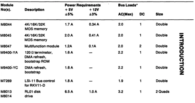
Table 1 Module Specifications
Option Module Power Requirements Bus Loads·
Deslg. No(s). Description +5V + 12V
±5% ±3% AC(Max) DC Size
H9281C 2 X 12 backplane 3.6 0
IBV11-A M7954 Instrument bus 0.8 A, 1.9 Double
Interface
-Z
KD11-F M7264 LSI-11 CPU with 1.8A 0.8A 2.4 Quad
-I
4KRAM
::D
KD11-H M7264-YA LSI-11 CPU 1.6A 0.25A 2.4 Quad
0
I\)
without RAM C
0
C
KD11-HA M7270 LSI-11/2 CPU 1.0A 0.22A 1.7 Doubl~
n
-I
-KDF-11 M8186 LSI-11/23 CPU 2.0A 0.2A 2.0 Double
0
KPV11-A M8016 Power-faillllne- 0.56 A 1.63 Double
Z
time clock
KPV11-B M8016-YB Power-fall/llne- 0.56 A 1.63 Double
time clock/120
n
bus terminator
* These ac load figures were measured using standard TOR (time domain reflectometry) techniques. The conversion factor is 9.35 pF/ac
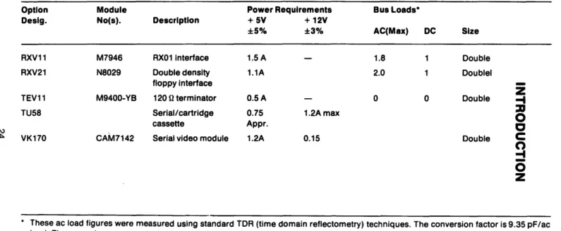
Table 1 Module Specifications
Option' Module Power Requirements Bus Loads*
Deslg. No(s). Description +5V + 12V
±5% ±3% AC(Max) DC Size
KPV11-C MS016-YC Power-fall/llne- 0.56 A 1.63 Double
time clock/220
n
bus terminatorKUV-11 MS01S WCSmodule 3.0A Quad
KWV11-A M7952 Programmable 1.75A 0.01A 3.4 Quad
Z
-I
real-time clock
::D
LAV11 M7949 LA 1S0 line printer O.SA 1.S Double
0
I\)
0
~
Interface
C
LPV11 MS027 LA1S0/LP05 O.SA 1.4 Double
n
printer Interface
~
MMV11-A G653 4KX 16 core 1.91 2 Quads
0
Z
memory
(standby current) 3.0A 0.2A
(operating current) 7.0A 0.6A
MRV11-AA M7942 4K X 16 read-only 0.4AA 1.8 Double
memory (less PROM Integrated circuits)
Table 1 Module Specifications
Option Module Power Requirements Bus Loads·
Deslg. No(s). Description +5V +12V
±5% ±3% AC(Max) DC Size
(with 32512 X 4 2.SA
PROM Integrated
clrcuts)
-(MRV11-AC)
Z
MRV11-BA MS021 UVPROM- O.5SA 0.34 A 2.8 Double
....
:IIRAM (less PROM
0
Integrated circuits) C
I\;)
C
I\;)
(with 81KXS 0.62 A O.5A
n
PROM Integrated
....
circuits)
(5
(MRV11-BC)
Z
MRV11-C M8048 PROM/ROM module O.SA 2.0 Double
MSVll-B M7944 4K X 16 read/write 0.6A 0.54 A 1.9 Double
MOSmemory
MSVll-CD M7955-YD 16K X 16 read/write 1.1 A 0.54 A 2.3 Quad
MOSmemory
Table 1 Module Specifications
Option Module Power Requirements Bus Loads*
Deslg. No(s). Description +5V +12V
:5% :3% AC(Max) DC Size
MSV11-D MS044 4K/16K/32K 1.7 A 0.34 A 2.0 Double
MOSmemory
MSV11-E MS045 4K/16K/32K 2.0A 0.41 A 2.0 Double
-
Z
MOSmemory
...
MXV11-A MS047 Multifunction module 1.2A 0.1A 2.0 2 Double ::II
0
I\J REV11-A M9400-YA 120
n
terminator, 1.6A 2.2 Double0
w DMA refresh,
C
bootstrap ROM
n
REV11-C M9400~YC DMA refresh, 1.6A 2.2 Double
:::!.
0
bootstrap
Z
RKV11-D M7269 LSI-11 Bus control 1.SA 1.9 Double
for RKV11-D
RLV11 MS013 RL01 disk 6.5A 1.0A 3.2 2 Quads
MS014 drive
I\J
.:=.
Table 1 Module Specifications
Option Module Power Requirements Bus Loads·
Deslg. No(s). Description
+
5V+
12V±5% ±3% AC(Max) DC Size
RXV11 M7946 RX01 interface 1.5A 1.8 Double
RXV21 N8029 Double density 1.1A 2.0 Doublel
floppy Interface
-Z
TEV11 M9400-YB 120
n
terminator 0.5A 0 0 Double ~TU58 Serial/cartridge 0.75 1.2A max
:II
0
cassette Appr.
C
VK170 CAM7142 Serial video module 1.2A 0.15 Double
C
n
::!
0
z
* These ac load figures were measured using standard TOR (time domain reflectometry) techniques. The conversion factor is 9.35 pF/ac
INTRODUCTION
CONFIGURATION
The LSI-11 bus permits a unified addressing structure in which con-trollstatus and data registers for peripheral devices are directly ad-dressed as memory locations. All operations on these registers, such as transferring informaton to or from them or manipulating data within them, are performed by normal memory address instructions. The use of memory address instructions on peripheral device registers greatly Increases the flexibility of input/output communications.
Addresses
~
a.430~·010
(EXT.LGTIl) 219
i.OIO
061
fOlD
,. IO~7'··"---....J
IQUAD "KG"':) .,
t---~c_--5.250____+_!
7451,.
(DUlllH)
-1
"'~
- - - + +--~I--~
1 _ 10.312 •
I
(QUAD. HIlT) - :
Figure 1
'.958.
(StD, LIllH)
Module Dimensions
ICJ1Q:
I*ENSIDIIS DENDTED II\' • AIlE FOR
MAX USEA8.£ CIRQIJT AREA, ~~.rcALL
IIDTlOIICW FINGERS lOTOPCWIWIIL£
8.M! OI0(£XT LOTH) 5.50!.DfO (STD LOTH)
I
1
:l
I :
: I
I :
: I
I :
!
I
I :
~ ~:
~
:.J
*J
~~a75~w.L:I ~;,..
z
....
:D
o
C C
n
::!
o
INTRODUCTION
Control and Status Registers
The general form for the control and status registers, shown In Figure 2, does not necessarily apply to every device, but Is presented as a guide.
15 12 11 10 8
T
ERRORS
BUSY
7 6 5
DONE OR READY
INTERRUPT ENABLE
4 3
T
DEVICE FUNCTION
o
ENABLE
Figure ~ Control and Status Registers
Many devices require less than 16 status bits. Other devices will re-quire more than 16 and therefore will rere-quire additional status and control registers.
The bits in the control and status registers are generally assigned as described below.
Typical Control and Status Register Bit: 15-12 Name: Errors
Function: Generally there Is an Individual bit associated with a spe-cific error. When more bits are required for errors, they can be ob-tained by expanding the error section In the word or by using another status word. Generally bit 15 Is the Inclusive-OR of all other error bits (If there Is more than one). Most devices will have "hard" error conditions which will cause an Interrupt If bit 61s set. Some may also have "soft" errors (warning types) which do not cause Immediate Inter-rupts.
Bit: 11 Name: Busy
Function: Set to indicate that a device operation Is being performed.
Bit: 10-8 Name: Unit Select
INTRODUCTION
Bit: 7 Name: Done or Ready
Function: The register ~an contain a done bit, a ready bit or a done-busy pair of bits, depending on the device. These bits are set and cleared by the peripheral device, but may be queried by the program to determine the availability of the device.
Bit: 6 Name: Interrupt Enable
Function: Set by the program to allow an interrupt to occur as a result of a function done or error condition.
Bit: 5-4 Name: Memory Extension
Function: Allows devices to use a full 18 bits to specify addresses on the bus.
Bit: 3-1 Name: Device Function Bits
Function: Specifies the operation that a device Is to perform. Bit: 0 Name: Enable
Function: Set to enable the device to perform an operation. Data Buffer Registers
The data buffer register Is used for temporarily storing data to be transferred into or out of the computer. The number and type of data registers is a function of the device.
Interrupts
Interrupts are requests, made by peripheral devices, which cause the processor to temporarily suspend Its present (background) program execution to service the requesting device. Each device that Is capable of requesting an Interrupt must have a user-supplied service routine that is automatically entered when the processor acknowledges the Interrupt request. After completing the service routine execution, pro-gram control Is returned to the Interrupted propro-gram. This type of oper-ation Is especially useful for the slower peripheral devices.
INTRODUCTION
Interrupt Vectors
An interrupt vector associated with each device is hard-wired into the devices's interface/controllogic. This vector Is an address pOinter that is transmitted to the processor duing the interrupt acknowledge se-quence, allowing automatic entry into the service routine without de-vice polling. The user can select an interrupt vector from the range of 000 to 777 for any interrupting options. The module can be configured to the desired interrupt vector by either selecting dip switches, con-necting or disconcon-necting wire-wrap pins, or installing or removing. wired jumpers on the module.
I
AAV11-A
AAV11-A 4-CHANNEL 12-BIT D/A CONVERTER
GENERAL
The AAV11-A is a 4-channel, digital-to-analog converter module that includes control and interfacing circuits. It has four 0/ A converters, a dc-dc converter that provides power to the analog circuits, and a precision voltage reference. Each channel has Its own holding register that can be addressed separately and provides 12 bits of resolution. These registers can be written and read, using either word or byte format. In addition, bits 0, 1, 2, and 3 of the fourth holding register are brought out to the I/O connector so they can be used as a 4-bit digital output register.
FEATURES
• Four 12-bit digital input channels, binary encoded for either unipolar mode or bipolar mode.
• Jumper-selected output ranges and modes: Bipolar mode ±2.56 V, ±5.12 V, ±10.24 V Unipolar mode 0 to +5.12 V, 0 to +10.24 V • One part in 4096 resolution
• 5V / itS slew rate
• ±5 mA drive capability per converter
SPECIFICATIONS
Identification Size
Power
Bus loads AC
DC
Resolution
Number of 0/ A converters Digital input
Digital storage
A6001 Quad
+5.0 Vdc ±5% at 1.5 A + 12.0 Vdc ±3% at 0.4 A
1.9 1.0
12-bits (1 part in 4096) 4
12-bits (binary encoded for uni-polar mode; offset binary encod-ed for bipolar mode)
AAV11-A
Output voltage range (jumper selected)
Gain accuracy
Gain temperature coefficient Offset temperature coefficient
Linearity
Oifferentiallinearity Output impedance Drive capability Slewing speed
Rise and settling time (to 0.1 % of final value)
DESCRIPTION General
±2.S6 V, ±S.12 V, ±10.24 V bipo-lar, 0 V to +S.12 V, 0 V to +10.24 V unipolar
Adjuatable (factory set for bipolar ±S.12 V)
10 PPM per °C, max.
20 PPM of full scale range per °C, max.
± 1f2 LSB max, non-linearity ± 1f2 LSB, monotonic 1 ohm max.
±6 mA max. per converter
S V/Jls
4 JlS (8 JlS wth SOOO pF load in parallel with 1 kO
(.)
U'I
-raU;"C;TROL
~
ILL~-J
I
~/I
I
~-,,-"
..
t...-"1IW
IJ
I
__ .
L... _ _ _ _ _ _ _ _
'---,
I r;;"'AC 1 a 2
I
I
I
(SAME AS DAC01I
I I
~
.-I
L _ _ _ _L ______ _
BSYNC L. BDOUT L. BDIN L. BWTBT L
-1.-L ______________
~READ DAC 3 H
11-00
READ OAC 3 L
I
WROAC3H T T ~/i '%
I
I,!!T U!;~
;
I
I
I
Figure 1 AAV11-ABlockDlagram
L ______
~---:J.~
<
...
AAV11·A
Bus Interface
The logic associated with the bus Interface section maintains proper communications protocol between the processor lSI-11 bus and the AAV1 1-A. This logic generates and monitors the bus signals Involved during data transfers between the processor and the AAV11-A, permitting the AA V11-A to recognize when it Is being addressed by the processor (address defined by setting on the address switch pack) to accept Input data from the processor, and to output data to the processor.
Control Logic
The AA V11-A has no control/status register. The four digltal-to-analog converters continually generate voltages at their outputs that reflect whatever digital values have most recently been written Into their re-spective holding registers. The role of the control logic Is to make the necessary discriminations between requests to change the state of the holding registers (I.e., to write Into the holding registers), and requests to put the holding register contents onto the BD lines where they can be picked up through the transceivers by the processor.
DACs 0,1, and 2
Dlgital-to-analog conversion functions are performed In each of the four AAV11-A channels by Identical circuits:
• a holding register which stores the digital value output by the proc-essor
• a dlgltal-to-analog converter (DAC) proper which generates a cur-rent that Is a function of the holding register value and of the modellevel jumper conditions
• an amplifier that translates the current Into a proportional voltage, provides a low output Impedance for the channel, and permits ad-justment of signal offset
DAC3
DAC 3 Is Identical to DACs 0, 1, and 2 except that holding register bits 0-3 are routed to the 110 connector as well as to the DAC. This ar-rangement permits these bits to be routed to external equipment that requires binary control signals at programmable Intervals. Control
CONFIGURATION
General
AAV11-A
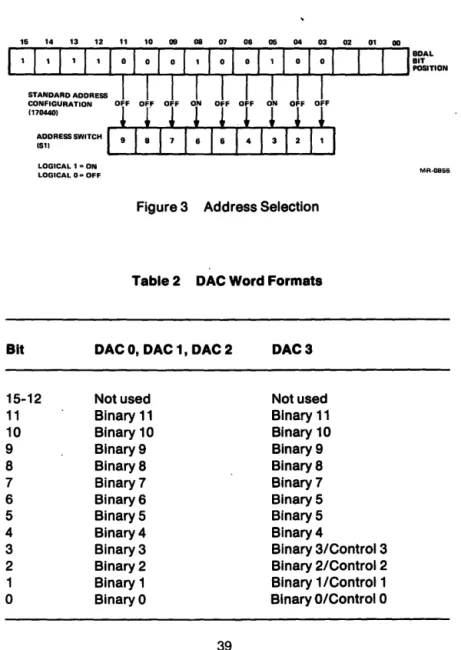
This section describes how the user can configure the module to func-tion within his system by setting dip switches (Figure 2) to obtain the desired device address. The voltage range for each 01 A converter (OAC O-OAC 3) can be configured independently by installing or removing the designated jumpers (Figure 2) associated with a specific 01 A converter. This section also describes how to connect external devices to the module. The standard factory addresses for the registers are listed in Table 1.
Table 1 Standard Addresses
Register Mnemonic Address
Holding 0 OACO 170440
Holding 1 OAC1 170442
Holding 2 OAC2 170444
AAV11-A
OAC0 OAC I OAC2 OAC3
c
JI1
DO
DO DODD
R l
~34
R i~5
Risi \
\ 3 7 (GAIN) (OFFFETI (GAIN) (OFFSET) (GAINHGAIN)(OFFSET0-I
OAC 0I I
OAC II I
OAC 2I I
RO:C(O:FST~ ~.!!1- ~ ~..!!!.!... .!!!.. ~ 0 - - - 0 0 - - - 0 Oo-CI 0----.0 0----.0
W6 W4 we W9 WI3 WI4 WI7 WI6 MODE I LEVEL STRAPS
BIT 3 BIT" \ SI /
c=J
(ADDRESS)Figure 2 AAV11-A Connectors, Switches, and Jumpers
Device Registers
The device registers can be configured to respond to any address within the range 170000 to 177777. Each register address does not have to be individually set. The DAC 0 register address is selectable and the last digit will be zero. The remaining registers will use ad-dresses 17XXX2, 17XXX4, and 17XXX6 for DAC 1, DAC 2, and DAC 3 registers, respectively. The factory-configured device address is 170440 as shown in Figure 3. The word formats for the DAC registers are described in Table 2. Note that all device registers are always a sequence of four consecutive even locations. There is no vector used for this module.
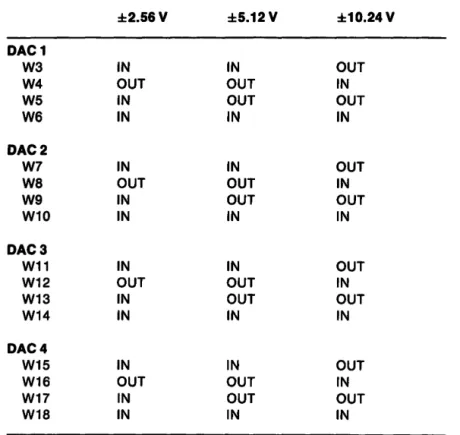
D/A Converter Range and Mode
AAV11-A
ry-configured for -5.12 to +5.12 V bipolar operation. The jumper configuations for the bipolar mode ranges are shown In Table 3; the unipolar ranges are shown in Table 4.
I :',
:4, ',' , :'
1
~
1
"I : 171 : 1
:'17, : 1
: 1
"I"I"I~~
..
STANDARD ADDRESS
I I I I I I I I I
Bit
CONFIGURATION OFF OFF OFF ON OFF OFF ON OFF OFF
(1704401
+
*
+ +
+
L
! !
i
~~~RESS
SWITCHI
9I
8I
7I
8I
8I
4I
3I
2I ' I
LOGICAL 1 ~ ONLOGICAL 0 DOFF
Figure 3 Address Selection
Table 2 DAC Word Formats
DACO, DAC1, DAC2 DAC3
15-12 11 Not used Binary 11 Binary 10 Binary 9 Binary 8 Binary 7 Binary 6 Binary 5 Binary 4 Binary 3 Binary 2 Binary 1 Binary 0 Not used Binary 11 Binary 10 Binary 9 Binary 8 Binary 7 Binary 5 Binary 5 Binary 4 10 9 8 7 6 5 4 3 2 1
o
39
Binary 3/Control 3 Binary 2/Control2 Binary 1/Control1 Binary O/Control 0
AAV11-A
Table 3 Jumper Configurations for Bipolar Operation
±2.S6V ±S.12V ±10.24 V
DAC1
W3
IN
IN
OUT
W4
OUT
OUT
IN
W5
IN
OUT
OUT
we
IN
IN
IN
DAC2
W7
IN
IN
OUT
W8
OUT
OUT
IN
W9
IN
OUT
OUT
W10
IN
IN
IN
DAC3
W11
IN
IN
OUT
W12
OUT
OUT
IN
W13
IN
OUT
OUT
W14
IN
IN
IN
DAC4
W15
IN
IN
OUT
W16
OUT
OUT
IN
W17
IN
OUT
OUT
AAV11-A
Table 4 Jumper Configurations for Unipolar Operation
OV-+S.12V OV-+10.24V
DAC1
W3 IN IN
W4
OUT
OUT
W5 IN
OUT
W6
OUT
OUT
DAC2
W7 IN IN
W8
OUT
OUT
W9 IN
OUT
W10
OUT
OUT
DAC3
W11 IN IN
W12
OUT
OUT
W13 IN
OUT
W14
OUT
OUT
DAC4
W15 IN IN
W16
OUT
OUT
W17 IN
OUT
W18
OUT
OUT
J1 Output Connections
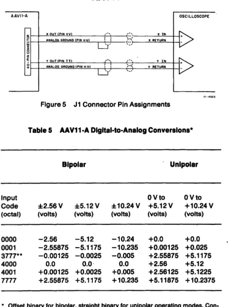
con-AAV11-A
nected to the AAV11-A logic ground, J1 pins L, N, R, or T. Note that the foregoing assumes that the LSI-11 power suppy ground is connected to power line (earth) ground. If continuity checks reveal no such connection, attach a length of 12-gauge wire between the power sup-ply ground and a convenient point associated with earth ground. Oscilloscope X and Y inputs may be either differential or single-ended. Differential inputs should be driven as in Figure 4.
M
w
AA CC EE OAC I HQ GNo HH KK
oAC 2 HQ GNo MM OAC 3 HQ GNO
-15V TEST PP SS +15V TEST OAC 0 HQ GNo UU
BOARO SlOE J 1
DO BIT 3 OUT FF BIT 2 OUT JJ BIT lOUT LL BIT 0 OUT NN oAC 3 OUT RR oAC 2 OUT TT
oAC lOUT VV OAC 0 OUT
Figure 4 Connection to Oscilloscope with Differential Input
AAV11·A
and line frequency errors which are due to ground voltage differences. The effect of magnetic coupling into the oscilloscope Input lines can be minimized for
a
differential-Input oscilloscope by running the AAV11-A output and its return line In a twisted pair. No benefit Is derived from a twisted pair with a single-ended oscilloscope Input. The effect of electrostatic coupling Into the oscilloscope Input lines can be minimized by shielding the Input lines from AAV11-A to the oscilloscope. The shield should be connected to ground at one end only. Grounding the shield at both ends may result in a ground loop which will adversely affect oscilloscope control results and any ADV11-A AID operations (If used).Careful selection of cabling is essential. The 0/ A outputs are capable of driving a maximum of 5000 pF. Output Impedance is 1 ohm. Output current limit is 5 rnA.
Optional Equipment
Figure 5 iIIustrat~s the H854 40-pin connector pin aSSignments for user outputs. These pins may be connected to the optional H322 dis-tribution panel for convenient user access via an optional BC08R cable. The optional BC04Z is available for applications which require an unterminated cable. One end is terminated with an H856 connector that mates with the H854 connector on the AA V11-A module. The other end is an unterminated ribbon cable. The BC04Z cable is avail-able in lengths of 3.05 m (10 ft), 4.5 m (15 ft), and 7.6 m (25 ft).
PROGRAMMING
All four OAC holding registers are automatically set to zero on system initialization. This produces -:-5.12 V at the OAC outputs when the mode/level jumpers are connected as delivered from the factory. Any holding register value remains In effect until changed by· the processor in response to a program instruction. Coding to the 0/ A converters is offset binary for bipolar operation and straight binary for unipolar operation. Offset binary defines 0 as maximum negative voltage, mid-point (I.e., 4000, for the 12-blt AAV11-A) as 0 V, and all1s (7777,) as maximum positive voltage. These relationships are Illustrated In Table
AAV11-A
AAVII-A OSCILLOSCOPE
II: X OUT (PIN VVI 1'--':, ,-, _ _ ---"-X =IN---+-I
II--I---'A""-NA~LOG~GR~OU:!!!JND~(!:.!!PIN~U~UI~r--'--:-_?:-: X RETURN
z ii:
*I--r-~~:=~~:=~~~~~-D(-PIN-H-H-I--~~~~~·<~--Y-R-E~LU~~:~~
Figure 5 J1 Connector Pin Assignments
Table 5 AA V11-A Dlgltal-to-Analog Converslons*
Bipolar , Unipolar
Input OVto OVto
Code ±2.56 V ±5.12V ±10.24 V +5.12V +10.24 V (octal) (volts) (volts) (volts) (volts) (volts)
0000 -2.5'6 -5.12 -10.24 +0.0 +0.0 0001 -2.55875 -5.1175 -10.235 +0.00125 +0.025 3777** -0.00125 -0.0025 -0.005 +2.55875 +5.1175
4000 0.0 0.0' 0.0 +2.56 +5.12
4001 +0.00125 +0.0025 +0.005 +2.56125 +5.1225 7777 +2.55875 +5.1175 +10.235 +5.11875 +10.2375
* Offset binary for bipolar, straight binary for unipolar operating modes.
Con-versions may be made between 2's complement signed binary and offset
binary numbers by subtracting 4000. from the 2's complement number (or
adding 4000. to the offset binary number) and using only the low-order 12
bits of the result.
ADV11-A
ADV11-A ANALOG TO DIGITAL CONVERTER
GENERAL
The ADV11-A is a 12-bit successive approximation analog-to-digital converter that samples analog data at specified rates and stores the digital equivalent value for processing. A multiplexer section can ac-commodate up to 16 single-ended or 8 quasi-differential inputs. The converter section uses a patented auto-zeroing design that measures the sample data with respect to its own circuitry offset and therefore cancels out its own offset error.
AID conversions are Initiated by program command, clock overflow, or external events. The program control Is determined by the control and status register (CSR). The clock overflow command Is supplied by the KWV11-A option. External event inputs can originate at the user's eqUipment or from the Schmitt trigger output on the KWV11-A clock. The digital data output Is routed through a buffer register to the bus, from which it can be transferred into memory. This buffer optimizes the throughput rate of the converter.
Three reference signals are provided for self-testing on any channel input: two dc levels and one bipolar triangular waveform. This output can be used with DIG IT AL diagnostic software to produce a data base for extremely thorough and preCise analog linearity testing.
FEATURES
• 16-channel multiplexer • Sample-and-hold functions • Auto-zeroing technique • Buffered data output • Self-testing features
SPECIFICATIONS
Identification Type Power
Bus Loads AC DC
A012 Quad
+5 Vdc ±5% at 2.0 A +12 Vdc ±3% at 450 mA
ADV11-A
Inputs
Analog input protection
Logic input protection
Analog input full scale range (FSR)
Analog inpul.dynamic resistance (Vin ::s;; 5.12 V)
Analog input bias current ( Vin ::s;; 5.12 V)
Logic input voltages
Logic input currents
Logic input riselfall time
Coding
AID Converter Resolution
Format
Fusible resistor guaranteed to open at ±85 V within 6.25 sec-onds. Guaranteed not to open from -25 V to +20 V at the input Overload affects no components other than the fusible resistor on the overloaded channel; no other channels are affected.
Fusible resistor guaranteed to open at ±25 V within 6.25 sec-onds. Guaranteed not to open from
-4
V to+9 V
at the input.10.24 V bipolar (-5.12 V to +5.12 V)
100 Mn minimum 50 nA, maximum Low = 0.0 to +0.7 V High = +2 V to +5 V Low = -6.8 rnA at 0 V High = +1.3 rnA at +5 V 400 ns maximum
12 bits, binary weighted (2.5 mV nominal)
Parallel offset binary, right justified
Input Voltage
+FS-1 LSB
o
-FS
Output Code 7777
4000
Vernier DIA
Resolution Format
Performance Gain error Offset error Differential linearity
Integral linearity
Temperature coefficients
Noise
Warm-up time Tlmlng_ External start
ADV11-A
(FS
=
5.12 V; 1 LSB=
2.5 mV)8 bits, binary weighted Offset binary encoded Input Code
377
200
o
Approximate Offset Voltage
+2.5 AID LSB (+6.4 mV)
o
-2.5 AID LSB (-6.4 mV)
Adjustable to zero Adjustable to zero
No skipped states; no states wid-er than 2 LSB. 99% of state widths ± 1h LSB
± 1 LSB, maximum non-linearity (referenced to end p-olnts) Gain = 6 PPM per °C
Linearity
=
2 PPM of full-scale range per °COffset
=
7.5 PPM of full-scale range per °CModule
=
0.4 LSB rms; 2 LSB peakSystem
=
0.5 LSB rms; 2 LSB peak5 minutes, maximum
ADV11-A
Synchronization Conversion time Transition interval
(reacquisition interval between end of conversion or channel change and start of new conver-sion)
Test Signals
OtoT
16 T (T
=
Clock period=
2 "s) 9"s
The ADV11-A provides three output voltages for test purposes: 1. Positive dc level, +4.4 V (±15%)
2. Negative dc level, -4.4 V (±15%) 3. Triangular wave, 15 Hz nominal (±15%)
DESCRIPTION
General
~
<0
~H:;N~ ;;L~T~ - - - . .
I
LOW CHANNELI
I
SELECTI
I
ENA~~~f1
I
I
_ _ . L AUTO-ZERO ~I
r,---,
• A-D CONVERSIONI
I
COMP HI
I
I~D~ ~
I
I
r - - - l " " " ' _I
I
I
I
I
I
I
I
_ _ _ _ _ _ _ _ .J
rcONTROL - - - ,
.
,LOW
I
CHANNEL SELECT
I
HIGH CHANNEL
I
SELECT :fr!ENABLE
I
ENABLEI
MISC.
CAOZC L CONTROL
I
LOGIC HOLD CNTL
I
VECTOR H
I
I
I
BUS MONITORS CONTROL-l..IIIIES
Figure 1 ADV11-A Functional Block Diagram
:.-c
<
...
...
•
:.-ADV11·A
Channel Selection
Channel selection is accomplished under program control by two 8-channel multiplexers and is a function of the data asserted in bits 8 through 11 of the control/status register (CSR). Each of the 16 analog input channels is routed to the single output channel through aMOS field-effect transistor which acts as a normally open switch. During the sample interval, the data pattern in CSR bits 8 through 11 selects one of these transistors and causes it to change from a condition of nearly infinite resistance (1 GU or more) to one of very low resistance (1000 U or less). Since in the selected state the transistor conducts current within the ±5.12 V limits equally well in both directions, it now func-tions as a closed switch, effectively routing to the output line whatever analog signal is connected to its input.
AID Conversion
AID conversion can be initiated in three ways: under program control, on overflow from the KWV11-A real-time clock, or on external input. When a conversion is completed or the control program writes
a
multi-plexer address into the CSR, the control logic initiates the transition interval, a delay of about 9 P.s to allow the multiplexer adequate selec-tion and settling time and to permit a valid representaselec-tion of the signal level to be established in the sample circuit. If no AID start signal has occurred by the time the transition interval has elapsed, the sample circuit merely follows the signal transmitted to it through the selected multiplexer channel and waits for an AID start signal. When an AID start signal occurs-or at the end of the transition interval if AID start was previously generated by the writing of the CSR GO bit-the sample-and-hold circuits are switched to hold, sustaining the sampled . level for the next step. The multiplexer output is then set to its hold condition, Le., to ground if the single-ended (SE) input is set low for single-ended measurement, or to the second differential input (return line) if the SE input is not set low. Note that if an external or clock start signal occurs during the transition interval, conversion starts immedi-ately, without waiting for the transition interval to be completed. Bit 15 of the CSR (AID Error) is set, however, and an interrupt is generated if Bit 14 (Error Interrupt Enable) is set-alerting the program that con-versions are occurring too fast and are consequently liable to be in error.digltal-ADV11-A
to-analog converter to generate an output equivalent to that produced by the hold circuits in response to a sample voltage of O. The digltal-to-analog converter output is summed with that produced by the hold circuits and with that coming from the grounded multiplexer output (single-ended mode) or from the second differential input (quasl-differential mode). If the current from the summing mode is negative, the first approximation was too low, and the comparator signals the SAR to maintain the state of bit 11 and repeat the process with bit 10. If the current from the summing mode is positive, the first approximation is too high, and the SAR changes the state of bit 11 before cycling to the second approximation. This process continues until all 12 bits in the word have been set, tested, and if necessary, changed. The 13th state (end of conversion, or EOC) indicates that the meas·urement is complete and that the SAR now contains an offset binary equivalent of the sampled voltage and may therefore be transferred to the proces-sor. EOC causes the sample-and-hold circuits to return to the sample mode and to reset the SAR, preventing further SAR activity until the occurrence of the next hold condition. .
Note that because the reference point against which the sample volt-age is compared is at the output of the multiplexer itself rather than internal to the sample-and-hold circuits, all offset voltages generated by the intervening circuits are common to both sample-and-hold con-ditions and are therefore cancelled out of any measurement. In slngle-ended mode, grounding the multiplexer output (and thereby esta-blishing this reference pOint) is identified as auto-zeroing the converter.
Bus Interface
transceiv-ADV11-A
ers are switches that let device and vector addresses be assigned to any given ADV11-A.
Control Logic
As the above discussion suggests, a large number of signals must be precisely orchestrated each time the ADV11-A executes a conversion. The control logic contains an assortment of gates, latches, read-only memories, and timing circuits designed to ensure that 1) multiplexer channels are properly selected, 2) sample durations are of adequate length, 3) conversions are not initiated during uncompleted previous conversions. In general, the user need not attend to any but the most elementary details of the conversion process, e.g., making necessary connections to the system and writing control programs that make appropriate use of the eSA.
CONFIGURATION General