l!11~~)I~A~,JIc:~:~=[iIt~I
®
TR.-l
c>
analog comp
uter
operator's hand
b
ook
ATTENUATOR
ROW
NON-LINEAR
ROW
AMPLIFIER
ROW
CON
TROL
PANEL
Of>
~'Q (
~
;
\0P~CE®
TR-1C>
quality engineered for simplicity and flexibility
•
Plug-in components
may be replaced easily and
quickly for expansion or servicing.
•
Non-linear components
fit most non-linear
row
po-sitions. Number of configurations is limited
only
by
the
number of components kept on hand.
•
Basic Computer
is pre-wired and can be expanded
simply by plugging
in
desired components -
no
additional wiring necessary.
•
Draws less power than 60 watt bulb.
Operates from
115V, 60 cycle outlet.
Bus bar power distribution
eliminates complex
cabling and simplifies
maintenance.
•
Solid
state design
-
instant warm-up - no
coolin
problems.
•
Human engineered
control
panel
is inclined for
easy, finger-tip
control.
•
Push button potentiometer
readout
system speeds
set up
-
reduces errors.
•
Built-in null voltmeter
provides
direct reading or
precision
null reading.
Interchangeable,
plug-in
components
add flexibility,
make expansion easy
COEFFICIENT
SETTING
POTENTIOMETERS
for inserting
equation coefficients
or problem
parameters into
computer.
COMPARATORS
compare a variable
input voltage to an
arbitrary bias
voltage and cause a
switching operation
to be performed.
TIE POINT
PANELS
provide
additional
patch panel
terminations for
components inputs
or outputs.
INTEGRATOR
NETWORKS
enable operational
amplifiers
to perform
integration.
FUNCTION
GENERATORS
electronically
generate analytic,
as well
as
arbitrary
functions of one
variable.
MULTIPLIERS
electronically
multiply two
variables of
either sign.
FUNCTION
SWITCHES
provide for
manually
interchanging
components
without
reprogramming or
repatching.
REFERENCE
PANEL
makes available
accurate reference
vol tages required
for problem
solution.
OPERATIONAL
AMPLIFIERS
are high-gain,
low-drift,
chopper-stabilized
DC amplifiers used
for addition,
subtraction,
integration and
inversion. With
other
components,
they also perform a
variety of
ACCESSORIES
~
; . . . • . .'0
,
'
"
• Service Shelf (Type 51.039) Facilitates maintenance of any plug-in computing component under normal operating conditions.
Feedback Resistor
Input Resistor
Diode Unit
Patch Cord
• Feedback Resistor
Type 646.010 - 10,000 ohms,
±
0.1% wire-round resistor; supplied in aBLUE
molded plug, is designed for patching between summing' junction and output terminations of any operational amplifier.• Input Resistors
Type 646.006 - 10,000 ohms,
±
0.1 %., anORANGE
banded epoxy-encapsulated, wire-wound resistor - male end plugs into amplifier summing junction termination, female end accepts patch cord plug.Type 646.007 - 100,000 ohms,
±
0.1%, aYELLOW
banded, expoxy-encapsulated, wire-wound resistor - male end plugs into amplifier summing junction termination, female end accepts patch cord plug.• Resistor Set (Type 5.134)
Includes the following quantities of Input and Feedback Resistors described above:
15 each Type 646.006 (see above)
10 each Type 646.007 (see above) 10 each Type 646.010 (see above) • Diode Unit (Type 614.051)
A WHITE banded, epoxy-encapsulated silicon diode for limiting the output of computing comp<Jnents or generating non-linear effects.
• Patch Cord Set (Type 5.133), includes the following: 10 each Type 510.033-0, 6" long, Color - Black 15 each Type 510.033-1, 12" long, Color - Brown 10 each Type 510.033-2, 18" long, Color - Orange
5 each Type 510.033-4,30" long, Color - Blue • Multiple Block (Type 542.605)
TR·l0 OPERATOR'S MANUAL
CONTENTS
INTRODUCTION
I.
THE COMPUTER
Introduction ... .
Attenuatars ... .
Operational Amplifiers. Type
6.112 -1 ... ..
Multiplier. Type 7.045 ... " ... .
Division ... .
X2 Diode Function Generator 16.101 ... ..
Log Diode Function Generator
16. 126 ... .
Variable Diode Function Generator 16.165 ... , .... .
Variable Diode Function Generators 16.154 and 16.156 ... .
Miscellaneous Devices and Patch Panel Terminations ... ..
Control Panel 20.344 ... ... .
Repetitive Operation ... .
II.
BASIC PROGRAMMING
System Equations ... .
Rearranging the Equations ... .
Block Diagram ... ... ..
Scaling ... ..
Computer Diagram ... ... .
Static Check Calculations ... ... .
Examples of Amplitude and Time Scaling ... .
Illustrative Examples ... .
Solution of Simultaneous Differential Equations ... .
A Non - Linear Problem ... ..
Generation of Analytic Functions ... ..
Transfer Functions ... ... ..
i I
I.
MISCELLANEOUS ADVANCED TECHNIQUES
Representation of Discontinuities ... .
Introduction to the Solution of Partial Differential Equations ... .
Introduction to the Solution of Algebraic Equations ... ..
APPENDIX I
Symbols for Computer Circuits ... ..
B
I BLI OGRAPHY
TR-l0 OPERATOR'S MANUAL
BAS I C PROGRAMM I NG PROCEDURES FOR
TRANSISTORIZED ANALOG COMPUTERS
INTRODUCTION
Many of the problems encountered in scientific or engineering endeavors require the solution of mathe-matical equations or sets of equations which in most cases are difficult and in other instances are, for all practical purposes, impossible to obtain by the classical approach to equation solution. The PACE TR -10 Analog Computer aids in overcoming this difficulty by providing the technical worker with a simple-to-use computer which permits the rapid solution of linear or non-linear mathematical equations.
Although the analog machine is correctly termed a computer, it does not perform its computations by numerical calculations as does the desk calculator or the digital computer. The analog computer per-forms mathematical operations on continuous variables instead of counting with digits. Thus the analog computer does not subtract 20 inches from 45 inches to obtain 25 inches but, rather, it subtracts 4 volts from 9 volts to obtain 5 volts. This answer the operator reads as 25 inches in accordance with his ar-bitrarily specified "scale factor" of 1 volt equals 5 inches. In the PACE TR -10, as is the case with the majority of modern analog computers, the continuous variables are d-c voltages.
The electronic analog computer makes possible the building of an electrical model of a physical system in which d-c voltages will behave with time in a similar way to the variables of interest in the actual system. If the vertical position of the center of gravity of an automobile oscillates with time during a disturbance, then the voltage representing the height of the center of gravity above the road surface will also oscillate; if the temperature of the coolant water at the exhaust port of the condenser rises exponen-tially to a steady value as a power plant is put into operation, then so will the voltage representing it on the computer. It can be said that the actual system and the electrical model are analogous in that the vari-ables which demonstrate their characteristics are described by relations which are mathematically equiva-lent. The actual system has thus been "simulated" because of the similarity of operation of the electric-al model and the actuelectric-al system. These capabilities of anelectric-alog computers are of great velectric-alue in performing scientific research or engin~ering design calculations in that they give an insight into the relationship between the mathematical equations and the response of the physical system. Although the analog com-puter operates as a simulator, it performs basically as an equation solver since it performs mathematical operations which result in solutions of the equations used to represent the actual system.
Although the analog computer utilizes electronic components and electrical circuit characteristics in its operation, it is not essential that its user have an extensive knowledge of electrical circuits. The task of preparing on the computer the correct electrical model is simple, and the steps necessary for accomplish-ing this task once the mathematical description of the primary system is known will be detailed in this manual. Once the electrical model is completed, experiments can be performed cheaply, quickly and with great flexibility to predict the behavior of the primary physical system under many different conditions, and it is with this in mind that one builds the model. The intention here is to give the scientist or engi-neer using an analog computer for the first time a comprehensive introduction to its functions, its mathe-matical programming, and its operation to achieve usable experimental results.
TR·l0 OPERATOR'S MANUAL
equations are usually differential equations having time as the independent variable. By applying appro-priate initial conditions and forcing functions to the electrical model, its behavior is determined to be the same as that of the primary system. This behavior is viewed through output devices which produce traces of voltage values plotted one against another on an x-y plotter or against time on a strip-chart recorder. Steady values of voltage are viewed on a voltmeter which is an integral part of the computer and can be connect-ed by a selector switch or by push buttons to the output terminations of many of the computing blocks.
TR.l0 OPERATOR'S MANUAL
I. THE COMPUTER
INTRODUCTION
The PACE TR -10 Analog Computer is a fully transistorized, general purpose analog computer. Solid state circuit elements are used throughout the computer to eliminate vacuum tubes, thereby achieving a compact design which requires very little power. It is able to operate stably and accurately in normal office sur-roundings. Reliable, with simplicity in functional design, it is easy to use and can be a powerful tool for the individual engineer in the rapid solution of scientific and engineering problems.
Consistent with our objective of programming the computer by interconnecting its components to solve mathematical equations, we will concentrate our attention on the computing components - the building blocks for our electrical model. These blocks are able to perform the following operations on variable d-c voltages - multiplication by a constant, algebraic summation, integration with respect to time, multiplica-tien of two variables, generation of known functions of a variable, or combinations of these operations. Each component has input terminations and output terminations which are readily accessible at the front face of the computer for interconnection by plugs and patch cords.
Below the patching area lies the monitoring and control panel. This contains features which permit (a) switching the computer on and off, (b) controlling the operational mode of the computer, (c) setting the values of problem parameters to three-place accuracy, (d) reading out stationary values of problem
vari-ables, and (e) periodically adjusting the balance of the d-c amplifiers to ensure their accurate operation.
The front face of the computer is divided into three five-inch high rows of computing components and their corresponding interconnecting terminations. This will be referred to as the "patch panel". In the top row there are attenuators for multiplying voltages by positive constants less than unity. In the bottom row there are high-gain d-c amplifiers uncommitted in their form of operation and, as we shall see later, capable of performing many tasks. In the middle row there is an assortment of components and terminations - integra-tor networks for use with the d-c amplifiers, fixed and variable function generaintegra-tors, quarter-square multi-pliers, comparators, and terminations for additional control p.anel mounted attenuators, function switches, the reference voltages of ±10. volts, and ground potential. These computing components will be the build-ing blocks in formbuild-ing any model and their characteristics and uses will be explained in sufficient detail to enable the reader to make use of them in his problems.
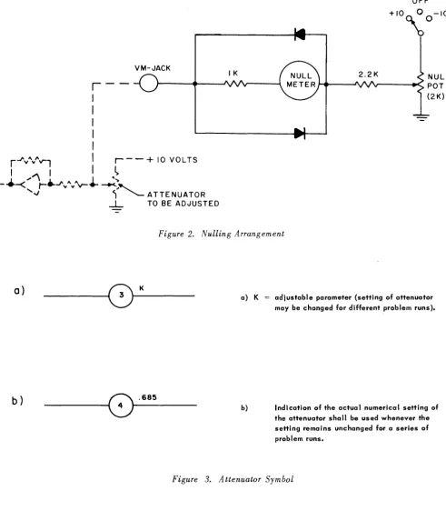
ATTENUATORS
Probably the simplest useful operation performed on the computer is that of multiplying a variable voltage by a positive constant whose value lies between zero and unity -- in electrical terminology, attenuation. A simple potentiometer is able to perform this task effectively to an accuracy of 0.1%. Thus, one is able to adjust problem equation coefficients and problem initial values by setting of the appropriate attenuator.
Four types of potentiometer modules are available, as shown in the accompanying Figure 1.
TR .10 OPERATOR'S MANUAL
orD
I
I
I
OlrD
"
II II
II
II I I
r---I:
.~
g
~
ATTEN. 42.183
@
@
AlTEN. 42.188
0
@
O@
~
~
+C
ATTEN. 42.187
PATCHING AREA
~
~
~
~
ATTEN12.265
@
~
@
~
@
~
@
~
ATTEN. 42.185
,,'-____
""" _----J'
VATTENUATOR GROUP TYPE 2.128
Figure 1. Attenuator Modules
TR·10 OPERATOR'S MANUAL
Attenuator 42.187. Same as for 43.183 except that in place of the second arm-termination q more convenient arrangement is available for adjusting the coefficient setting of the potentiometer. A push button is used to -replace the patched signal voltage input by + 10 volts and to connect the arm of the potentiometer to a Pot Set Bus. With the appropriate positioning of the Meter Mode Selector Switch this connects the output
of the attenuator directly to the voltmeter for suitable adjustment (discussed later). No auxiliary patching is required to adjust this attenuator accurately as is required for 42.183.
A ttenuator 42.188. Ten-turn, wire-wound potentiometers (5K ohms) with calibrated dials. Same as for 42.187 except for a change in the potentiometer used.
A ttenuator 2.128. This group of four ten-turn, wire-wound potentiometers (5K ohms) with calibrated dials is positioned at the right of the control panel. The potentiometer terminations are at the right side of the middle row of the patch panel. All potentiometers are grounded, having simply one input and an output ter-mination. Push buttons are available for ease in adjusting these attenuators and the. intention is that they be used in a computer model to effect changes in the important design parameters of an investigation.
Whenever the coefficient setting of an attenuator is to be adjusted with accuracy on the computer, an elec-trical check of the setting must be used. A mechanical adjustment could be inaccurate for a number of reasons. For a fair degree of accuracy, applying + 10 volts to the input and reading the output voltage on the voltmeter will be satisfactory, provided the intended connections from this attenuator to other compo-nents are complete and the potentiometer is therefore correctly loaded. For precision in setting the co-efficient value, a nulling arrangement must be used in which the voltage appearing at the output of the
at-tenuator is nulled against the output voltage from an unloaded, carefully aligned, precision ten-turn poten-tiometer.
The nulling arrangement for an attenuator type 42.183 is shown in Figure 2. A patch cord must be connect-ed from the arm of the attenuator to the VM - Jack on the control panel. A second cord must be usconnect-ed to con-nect + 10V reference voltage to the "high end" of the attenuator. With the meter mode selector switch in the NULL position and the reference switch associated with the NULL POT switched to the + 10 position, the attenuator can be adjusted until a null indication is obtained on the meter.
For the setting of attenuators Type 42.187, 42.188 and 2.128 (push button feature), a similar nulling arrangement is used with the exception that the operation of the push button will automatically accom-plish the equivalent of the two cable connections mentioned above. The attenuator will be supplied with
+ 10 volts, and its arm will automatically be connected to a POT BUS within the computer. Setting the meter mode selector switch to the POT BUS position will connect the nulling arrangement to the POT BUS. With the NULL POT reference switch in the + 10 position, a null will be obtained by adjusting the attenuator.
When setting a potentiometer it is important that the load be the same during setting as during use in the problem. In practice the load on an attenuator usually consists of a resistor connected between the poten-tiometer arm and an amplifier summing junction which rides at ground potential. In some cases it is pos-sible during the setting procedure to overload an amplifier so that its summing junction is no longer at ground. Should this happen, the overload alarm would sound and an incorrect setting would be made. To prevent this, the operator should ground the appropriate amplifier summing junction with a patch cord during the pot setting operation. The cord should be removed before proceeding with the problem.
TR ·10 OPERATOR'S MANUAL
r
I
I
I
I
I
VM-JACK
r-"vl\ .. /\,...,
I
r - -
+
10 VOLTSI
~
I
I
~
- +-<
~
re.
J " I\y"v-~
<I.,,> [image:13.615.50.542.89.652.2]... "
~"--
ATTENUATOR-L.
TO BE ADJUSTEDFigure 2. Nulling Arrangement
a}
b}
__________ ~~ .685a) K
b)
adjustable parameter (setting of attenuator may be changed for different problem runs).
Indication of the actual numerical setting of the attenuator shall be used whenever the setting remains unchanged for a series of problem runs.
Figure 3. Attenuator Symbol
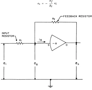
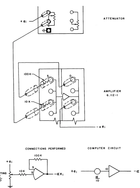
OPERATIONAL AMPLIFIERS TYPE 6.112·1.
TR·l0 OPERATOR-S MANUAL
amplifier consider the circuit shown in Figure 4, where the symbol containing -A represents a high-gain d-c amplifier. As is customary in all analog computing circuits, the voltages ei, eg, and eo are measure~
·with respect to a common ground potential. Applying Ohm's law to the input of the amplifier, one has summing currents:
Also, by definition of A: eo = -
A
eg
Now ig , the amplifier's input current, is extremely small compared with the currents flowing through
Ri
andR
f
giveu by the quotients involved in equation (1). Thus, one may approximate it as zero, and, combining the two equations, one has:(1)
(2)
(3)
But A, though dependent on frequency, has a value in the range of 104 - 107 for all expected computer
operations and, therefore, provided the ratio Rf is comparatively small (less than 100, say), one can write:
Ri '
r
FEEDBACK RESISTORRf
[image:14.612.143.463.391.706.2]o
Figure 4. Operational Amplifier
TR .10 OPERATOR'S MANUAL
Thus one obtains the most important result that, provided the input current is low and the amplifier gain is large and negative, then the output- input relation is solely dependent on the ratio of the feedback to the input resistors. By suitable choice of resistors or other impedances such as capacitors, many worthwhile relations can be obtained. A few of the more commonly required ones will be detailed in the following para-graphs.
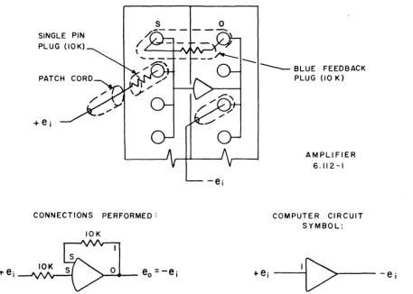
1. Sign - changing or Inversion
If both resistors are of equal value, 10K ohms say, the output voltage will be equal but opposite in sign to the input voltage.
(5)
Blue plugs containing 10K ohm resistors are available for connecting between the output and input ter-minations of a high-gain d-c amplifier, and single pin plugs containing 10K ohm resistors are available for use as input resistors. Thus the connection of a d-c high-gain amplifier for use as an inverter is as shown in the accompanying Figure 5. Two lOOK resistors may also be used to make an inverter. However, this is not generally recommended since better performance is obtained with the 10K -10K inverter.
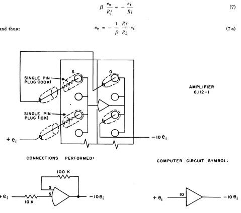
2. Multiplication
by
-10.If the feedback resistor has ten times the value of the input resistor, then the output voltage will be
op-SINGLE PIN PLUG (10K)
PATCH
CONNECTIONS PERFORMED:
10K
o
FEEDBACK (10 K)
AMPLIFIER 6.112-1
[image:15.618.85.543.353.680.2]COMPUTER CIRCUIT SYMBOL:
TR ·10 OPERATOR·S MANUAL
posite in sign and ten times the input voltage.
(6)
Single pin
lOOK
ohm plugs are available for use with the amplifiers and thus a connection as shown in the accompanying Figure 6 effects a multiplication by -10.3. Multiplication
by
a cons tant - a, 1<
a<
10.By the combined use of an attenuator and an operational amplifier, a multiplication by a constant between
-1 and - 10 can be obtained. Figure 7 shows the appropriate connections.
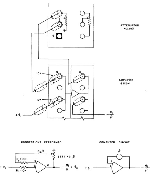
4. Division
by
a constant{3.
Division by a constant
(3
can either be treated as multiplication by 1/{3
or can be obtained with the cir-cuit shown in Figure 8. This circuit satisfies the relation:and thus: eo
CONNECTIONS PERFORMED:
100 K
eo
{3
- =Rf
(3
e' ~
Ri
Rf ei Ri
AMPLIFIER 6.112-1
(7)
(7 a)
~-... : . . . - - - + - - - - 10
e
iCOMPUTER CI.RCUIT SYMBOL:
- - - 4
10
[image:16.612.65.544.271.695.2]TR-10 OPERATOR'S MANUAL
ATTENUATOR
AMPLIFIER
6.112-1
' - - - a
e
iCONNECTIONS PERFORMED COMPUTER CIRCUIT
SETTING
ex:
10
[image:17.615.56.515.71.684.2]lOOK
'I~
CONNECTIONS PERFORMED
[image:18.615.75.558.87.667.2]SETTING:
f3
o
Figure 8. Division
by
a Constant +f3
TR ·10 OPERATOR'S MA~UAL
ATTENUATOR
42.183
AMPLIFIER
6.112 -I
COMPUTER CIRCU1T
e·
>-_ _
- - _
..::LTR -10 OPERATOR'S MANUAL
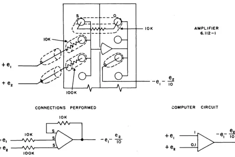
5. Summation of a Number of Voltages.
The inclusion of more than one input resistor to a high-gain d-c amplifier circuit, each resistor having a voltage applied to it, changes the original development of the input - output relationship to:
That is to say the current flowing through the feedback resistor must be the algebraic sum of currents flowing through the input resistors since the amplifier input voltage and current are zero.
Thus:
(8)
(9)
By using equal values for all resistors, one obtains a simple algebraic summation with the usual inversion associated with every computing amplifier.
If
the resistors have different values, then each input -voltage is multiplied by a factor given by the ratio of the feedback resistor to the input resistor before the sum is taken. 1£ both positive and negative voltages are applied to an amplifier, then due recognition to sign is paid in the algebraic summation process. See Figure 9.... +--+-IOK
+e.
CONNECTIONS PERFORMED
[image:19.615.58.533.367.684.2]10K
Figure 9. Operational Amplifier - Summing
AMPLIFIER 6.112-1
TR -10 OPERATOR'S MANUAL
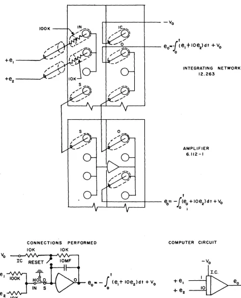
6. Integration with respect to time.
If the algebraic sum of the input currents is forced to pass through a feedback capacitor rather than a re-sistor, the current equation is:
(10)
This relation depends simply on the fact that when current passes through a capacitor the voltage across the capacitor changes with a rate proportional to the current. Integrating equation (10) and assuming an initial voltage across the capacitor of
Vo
gives:+ (11)
If C has a value of 10 microfarads and all input resistors have values of lOOK ohms., the expression for eo reduces to:
eo = -
f
t [e1 + e 2 + e3 + .... ] dto (12)
If an input resistor has a value of 10K ohms, then the corresponding input voltage is multiplied by 10 be-fore summation and integration.
It is necessary to be able to control the operation of integration and also to be able to apply an initial c'harge to the capacitor to set the initial value (Vo) of the output voltage eo. Thus, to form an effective in-tegrator more than a simple capacitive feedback is required. To effect integration on the TR -10, one connects an integrator network across a high gain d-c amplifier and the necessary input resistors are applied to that integrator network. Do not apply input resistors to the standard input terminations of the d-c amplifier for this would by-pass the most important "hold relay" in the integrator network (see later). The output voltage may be taken from either the network or the amplifier terminations. (See Figure 10).
With these six examples there has been demonstrated the versatility of the operational amplifier. To sum-marize, one might list the following operations as those performed by the unit when suitably connected with resistors and/or capacitor~.
a) Inversion
b) Multiplication by a constant greater than unity
c) Algebraic summation
d) Integration with respect to time of an algebraic summation
Th'e amplifier has uses other than those of directly effecting mathematical operations. By suitable analysis combinations of input and feed-back elements can be determined for developing with one amplifier many de-sired transfer relations. Frequently the amplifier is used without a direct feedback connection through a passive element but with a feedback path through oiher computing components. With this arrangement the amplifier brings about a null of the input currents by changing that one dependent on the feedback connec-tion. A simple example of this use appears later in the manual when the quotient of two variables is dis-cussed.
COMPUTER SYMBOLS
com-TR ·10 OPERATOR'S MANUAL
+e
~---+--- --Vo
[image:21.629.58.532.101.688.2]t
...
---:~--_+_--
e
o-{<e,t
loe
2)dt +Voo
+e,---'
2 10K
INTEGRATING NETWORK 12.263
AMPLIFIER 6." 2-1
t
. L . . . f o - - - I I - - -
eO = -
[(eo
+
10e2)
d t+
Vo
o j
CONNECTIONS PERFORMED COMPUTER CIRCUIT
10K JOK
t
eo· -
f
(e,1-
IOe2)dt+
Vo
oTR .10 OPERATOR·S MANUAL
puters, the symbols used to represent summing, integrating and high - gain amplifiers are given along with those of other devices in Appendix I on page 67.
CIRCUIT INFORMATION REQUIRED FOR THE APPROPRIATE OPERATION OF THE HIGH-GAIN D-C AMPLIFIER
For accurate computation the amplifier must remain balanced. It must produce a zero output voltage when the combined effects of the input voltages or the absence of all input voltages demands it. With this re-quirement in mind the amplifiers contain chopper stabilization circuits to minimize the effects of compo-nent drift. Under normal circumstances the amplifiers will remain balanced for periods of hours or days. However, at intervals it is necessary to check this condition, and if an amplifier is found to be unbalanced then an adjustment is recommended.
Below the control panel, hidden by a snap-fit cover plate, are the balance potentiometers for the amplifiers. With the Meter Mode Selector Switch in the position "BAL", each amplifier can be selected on the Ampli-fier Selector Switch and its balance tested and trimmed. When making this adjustment, it is necessary for all amplifiers to have a feedback connection of some form.
In normal use the deflection of the balance meter should be adjusted to within two or three divisions of zero. When first turned on, the deflections may be slightly higher but will return to their normal levels after 30 or 60 minutes warm-up. For unusual problems which might be sensitive to amplifier unbalance or integrator drift, amplifiers may be balanced at more frequent intervals so as to keep the meter deflection below one division.
The operation of the computer is intended to accomodate signal voltages having values up to a maximum of the reference voltage ± lOVe Under some conditions the amplifiers can produce output voltages as high as
± 14V, but for accurate, reliable computation they should not be required to give more than ± 10V. An over-load alarm feature is included in the computer which indicates the presence of an overover-loaded amplifier, usually due to a patched circuit requiring too large an output voltage. The overloaded amplifier may be lo-cated by placing the meter select switch in the BAL (balance) position and rotating the AMP (Amplifier Selector) switch until a large meter deflection is noted. The overload alarm does no more than indicate that something is wrong with the patched circuitry, the problem operation or the components. It is well to note that occasionally an overloaded amplifier will cause no appreciable error in a problem solution and then there is no need to take any corrective action. However, the operator should ascertain that this is the case before proceeding with the problem.
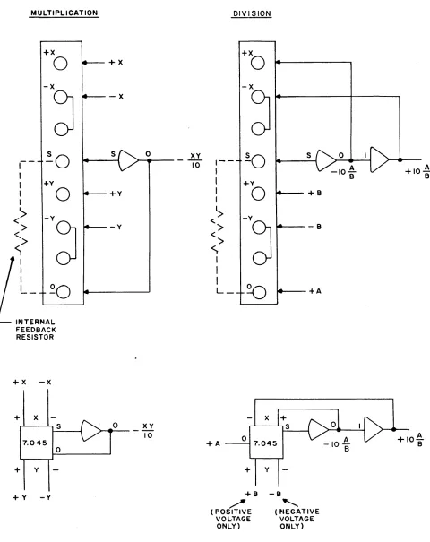
MULTIPLIER, TYPE 7.045.
Multiplication of two variable voltages is a non-linear operation which is necessary on a general purpose computer. A "quarter-square" technique is used to effect this operation, use being made of the identity:
XY
-I [ (X + y)2 - (X - Y)2 ] (13)4
The squaring operations are performed by fixed DFG's of the type described later, and interconnected circuitry within the unit requires only that the connections shown in figure 11 be made to the patch panel terminations for this unit. All four inputs (+ X, - X, + Y, - Y) must always be patched in even though one or both of the inputs may not change sign during a problem run. Note that the output voltage from the re-quired associate amplifier is -XY /10. A. change in the output to +XY /10 is accomplished easily by inter-changing the +X and -Y inputs, or +Y and -Y inputs.
TR ·10 OP ERATOR'S MANUAL
MULTIPLICATION
+x
0
+x -xJ
- x':0
S,--,
,
+YI
0
+YI
>
-VJ
<
>
-Y<.
>
~
I I IL_
~O
INTERNAL FEEDBACK RESISTOR
+x - x
+ X
S 0
7.045 0
+ Y
+Y -Y
0 XY
10
XY
10
DIVISION
1
-I
I
,
I'>
<
>
<
>
<;
II
I
L_
+A +x0
-xJ
~O
S+Y
0
+B-V
J
-B~
+Ax
+
r-'---'-, S t - - - - i
o
7.045+
Y+8 -8
",/'
[image:23.588.54.534.80.685.2]
'-( POSITIVE VOLTAGE ONLY) ( NEGATIVE VOLTAGE ONLY)
Figure
11.
Multiplier 7.045 Connections+IO~
B
TR -10 OPERATOR'S MANUAL
DIVISION
When it is necessary to divide one variable voltage A by a second variable voltage B, one uses a multi-plier in the feedback circuit of a high-gain amplifier. Consider the computer-circuitry shown in Figure 11.
Assume the output voltage of the high-gain amplifier to be C. Then at the grid of the amplifier the null relationship
CB
+
A
o
(14)10
is satisfied by automatic changes in the value of C. Hence,
C
=-lOA
B
(14a)
A most important point to note about this circuitry is that although the voltage A can have both positive and negative values, the B voltage must always have positive values. Should B always be negative, then the use of - B in its place, (i.e., the interchange of the connections to + y and - y), will produce at the output of the high-gain amplifier,
C + lOA (14b)
B
One must place the following restrictions on the voltages in a quotient:
1. The absolute value of the divisor B must always be greater than or equal to the absolute value of the dividend A, otherwise an overload may occur in the output amplifier.
2. The divisor B must not change sign. It must not pass through zero, for this would imply an in-determinate or infinite quotient. Moreover, the circuitry requires that the high-gain amplifier be surrounded by negative feedback, and this can only be arranged for one or other sign of the B voltage. If B is a negative voltage, then + Band - B are interchanged and the output of the
high-. l · f · · h lOA h h lOA
gam amp 1 ler IS t en
+ - -
rat ert an- - - .B B
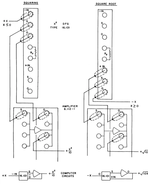
X2 DIODE FUNCTION GENERATQR, TYPE 16.101.
As another example of the non-linear function generating equipment available in the computer, we will con-sider briefly the X2 DFG. Using resistors and solid state diodes, this unit generates two quadratic curves, one for positive input voltages, the other for negative input voltages. Each curve is made of seven straight-line segments approximating the function X2. When used with an operational amplifier the section termin-ated on the upper part of the X2 DFG module accepts a negative voltage X and produces a positive volt-age X2/10. Should X be a positive voltage, the output will be zero. The section terminated on the lower part of the
X2
DFG module accepts positive voltagesX
and produces from the associated operational amp-lifier a negative voltage - X2/10. Should X in this case be a negative voltage, the output will be zero.The patching interconnections required to obtain various types of mathematical functions with the X2 DFG are shown in the accompanying figures 12 and 13. The symbol for use in a computer circuit diagram is shown in Appendix I, page 67.
LOG DIODE FUNCTION GENERATOR, TYPE 16.126
A second frequently occurring non-linear function which can be generated with a component available in the computer is the logarithm. Employing the same kind of circuitry as the
X2
DFG, the LOG DFGTR -10 OPERATOR'S MANUAL
SQUARING
+X
X ~O
~
OJ
+IN
0
So
'b
+X
SQUARE ROOT
-IN
0
X2 DFG
So
TYPE 16,101
°0
~
-x
AMPLIFIER X~O
6.112-1
~--..--..----~---+~
COMPUTER
[image:25.591.50.540.81.693.2]CIRCUITS - X - - 0 ...
6+,N
D...;:S---fC>~O--.-
I
+./IOX
X
SQUARING POSITIVE OUTPUT
±INPUT
-IN
0
So
0
0
~
+IN
0
S
S
0
0
0
0
X
X
X2
+1"0
SQUARING NEGATIVE OUTPUT
±INPUT
-IN
-
0
So
0
0
L...~-+IN
...
0
So
..
0
0
..-Figure
13.
X2 DFG ConnectionsTR .10 OPERATOR'S MANUAL
S
0S
0 [image:26.594.85.545.81.698.2]TR-10 OPERATOR'S MANUAL
cepts a voltage X with magnitude between 0.1 and 10 and with the aid of an output amplifier produces a voltage proportional to Log1o [10
I
XI].
Each module contains two separate function generator circuits;one terminated on the upper half of the face of the module accepts negative voltages X and produces Y::: +5 Log1o[10 IXI], the other terminated on the lower half of the face of the module accepts positive
voltages X and produces Y::: -5 Log1o[10 IXI]. For either section the absolute value of X should normally
be restricted to lie in the range 0.1 ~ IXI ~ 10. Although input values between 0 and 0.1 may be used, accuracy limitations with low value inputs limit the usefulness of the answer.
The normally required connections for the unit are shown in Fignre 14.
Just as the X2 DFG can be used to produce its inverse, the square root, so the Log DFG can be used to produce the Antilog, see Figure 15* By using three Log DFG's and one amplifier, multiplication of two variables, neither of which change sign, is achieved. Similarly, one can obtain the quotient of two
variables neither of which change sign. The use of one more DFG section allows either the multiplication or the division of a quotient by a third variable.
VARIABLE DIODE FUNCTION GENERATOR 16.165
In many investigations the dependence of one variable quantity Y on another quantity X is known only in the form of an experimentally - determined curve. For example, the drag coefficient of an airfoil is determined from wind tunnel experiments to be dependent on the air speea, but the dependence is known only as a table of corresponding values or as a graph of drag coefficient versus Mach number. The specific heat or thermal conductivity of a plastic material might be non-linearly dependent on the tempera-ture of the material and this dependence might well be known, not as a neat algebraic relationship, but as a graph of corresponding values. These coefficients and their dependence on the appropriate variable, be it velocity, temperature, or any other quantity, must be included in any computer study of the physical system. Their somewhat irregular dependence makes it desirable to have available in the computer a device which will accept a voltage representing, say, Mach number and give out a voltage representing the drag coefficient. For a different problem this same device will accept a voltage representing
tem-perature and give a voltage representing thermal conductivity. The variable diode function generator is such a device, accepting a voltage X and when suitably adjusted, giving a voltage Y which is a required function of X; Y::: f(X).
Using the same techniques as the X2 and Log DFG's, the Variable DFG permits any function of the input voltage X to be represented by a number of straight line segments. Solid state diodes are biased to change their state of conduction, each at a different value of X as X changes from -10 volts to +10 volts. The breakpoints (i.e. the points at which the diodes begin conducting) are at selected values of X and are not adjustable by the user. Where each diode conducts, it contributes a current to the output of the DFG unit which is proportional to the input voltage X. The constant of proportionality for each current is ad-justable by a "SLOPE" potentiometer associated with each diode circuit. The sum of the currents con-tributed by the diodes is applied to the summing junction of an operational amplifier and thereby forced to pass through a resistor placed around the amplifier. Thus the output voltage of the amplifier changes with X along a sequence of straight line segments, the slope of any segment depending on the number of diodes that are conducting and the settings of the slope potentiometers associated with those diodes.
The variable DFG 16.165 has ten diodes with break points set at -9v, -7v, -5v, -3v, -lv, +lv, +3v, +5v, +7v, and +9v. Each has a slope potentiometer. The value of the output voltage Y::: f(X) at X = 0 can be set at any value between -10v and +10v by the PARALLAX potentiometer, and the slope of the curve at X ::: 0 can be set by the CENTRAL SLOPE potentiometer to have any value between plus and minus 2 volts per
*
Amplifier output signals are obtained by summing Amplifier input currents. The current output of the 16.126 Logx
-IO<X<-O.I
TR ·10 OPERATOR'S MANUAL
-IN X -IN
----I
I
OS 16.126 :
S
~5
LOG,o(IOIXIJ_Y _ _
+_I
N-II'
6. I 26. • >-.
----,-a. .. -
5 LOG 1o( 101Y!)I
s
Sc>
o
I
o
COMPUTER CIRCUITo
Y
»---II1II .... 0.1< Y<IO
S 0
0
+5 LOG1o(10 IXI)
NOTE:
0
0
AND LOG DFG AS SHOWN AUTOMATIC· THE CONNECTION OF AMPLIFIER ALLY CONNECTS A FEEDBACK RESIS-TOR OF 5000 OHMS.0
0
S 0
0
0
)4---.
-5 LOGIO(IOIYI) [image:28.595.100.528.95.687.2]o
0
TR ·10 OPERATOR'S MANUAL
o
1
I+~N
X
16.126 -IO<X<O
OR
01
I~N
X
16.126 O<X<+IO
(a) ANTILOG CIRCUITS
X +IN
16.126 S
Y
+
IN 16.126 S0.1< Y < 10
OR
X -IN
16.126 S -10 < X< -0.1
Y -IN
16.126 S -10< Y< -0.1
(b) MULTIPLICATION CIRCUITS
C>
C>
~ I
O+U
J
+10
ANTILOGr
~_l.. 10S
16.126
-10 VOLTS
.2-
16.126S S S
ANTILOG
O+U
-IN
-XV
> - - -...
----1.
10
+IN
..
5KV
+XY 10
+10 VOLTS
TR -10 OPERATOR'S MANUAL
Y +IN
16.126 0.1< Y< 10
x
-
IN16.126 -10< x< - 0.1
S S
16.126
S
+10 VOLTS
-IN
lOY
*
~----~----.
+
-X-Ixi
~
YOR
*'
SINCE THE SIGN OF THE QUOTIENT ; IS NEGATIVE, THE AMPLIFIER VOLTAGE IS NEGATIVE.Y tiN
16.126 0.1< Y< 10
x
-IN16.126 10< X<- 0.1
S S
16.126
S
-10 VOLTS
+IN
> - - -... - - . -lOX
*
Y
*'
SINCE THE SIGN OF THE QUOTIENT+IS NEGATIVE. THE AMPLIFIER VOLTAGE IS POSITIVE.(c) DIVISION CIRCUITS
Y tiN
16.126 0.1< Y<IO
Z +IN
16.126 I<Z<IO
X - IN
16.126 -10< X < -0.1
(d) COMPOUND MULTIPLICATION S
S
S
S -IN
~ 16.126
~
SJSV
*
SINCE THE SIGN OF THE QUOTIENT*
VZ +
-X
I I
X IS NEGATIVE, THE AMPLIFIER VOLTAGE IS NEGATIVE.TR·10 OPERATOR'S MANUAL
±IN
X-l~----+l
SI
II~
01
S2
x
IN16.165 . > - - - -Y= f (x)
COMPUTER CIRCUIT
0
0
0
0
O·
0
0
S 0
Y=f(x)
0
0
0
0
/0-
~Q
[image:31.599.68.492.91.680.2]~-Q
-
...,
TR -10 OPERATOR'S MANUAL
y= f (Xl
x
NUMBER OF
DIODES 5 4 3 2
o
2 :3 4 5CONDUCTING
Figure 17. Nonlinear Function Easily Generated by a Variable DFG
volt. The slope potentiometer of each diode allows the slopes of adjacent straight line segments to differ by any value up to 1 volt per volt.
For the generation of any arbitrary function, two uncommitted operational amplifiers are required to be connected to the v~riable DFG as shown in Figure 16. This arrangement would permit the function shown in Figure 17 to be generated quite easily.
[image:32.602.90.532.86.465.2]TR ·10
OPERATOR'S MANUAL
The following
steps
should be followed in preparing a variable DFG to give a desired function (see figures
18 and 19).
1. Prepare a table of the appropriate ly scaled voltages desired at the output of the DFG when the
input voltage
has
each of the following values:
-10, -9, -7, -5, -3, -1,0, +1, +3, +5, +7, +9
and
+10
volts. Note
that
the values at
-1,
°
and
+1
must be colinear.
2. Plug
the
VDFG into a service shelf and connect the required amplifiers appropriately to the
ter-minations
of
the unit. The VDFG potentiometers are now available for screw driver adjustment. Turn
all potentiometers fully counter-clockwise.
[image:33.788.178.601.320.887.2]3. Ground the VDFG input or set the input to zero and, by adjusting the PARALLAX potentiometer,
Figure
18.
Patch Panel Arrangement for Adjusting a Variable DFG
TR -10 OPERATOR'S MANUAL
10 K
+
10 VOLTS IN16.165
10K
S2
MONITOR THIS VOLTAGE AND ADJUST DFG
PRECISE INTEGRAL VALUES OF VOLTAGE
POTENTIOMETER TO OBTAIN THE
[image:34.589.54.539.87.536.2]REQUIRED VALUE
[1-5 VOLTS]
3.95
-+1 +3 +5 +7
[ ADJ UST POTENTIOMETER AT + 5 TO OBTAIN
+
3.95 VOLTS HERE]x
Figure
19.
Circuit for adjusting a Variable DFGobtain the appropriate output voltage f (0) from amplifier 2. Use the procedure detailed later on page 32 to check this voltage.
4. Apply -1 volt to the VDFG input and- adjust the potentiometer labeled "-1" until the output of amplifier 2 reaches the value £(-1).
5. Apply -3 volts to the VDFG input and adjust the potentiometer labeled "-3" until the output of amplifier 2 reaches a value f (-3).
TR·l0 OPERATOR'S MANUAL
Input Voltage Adjust SLOPE To obtain amplifier 2 potentiometer labeled output voltage
-5 volts -5 volts f(-5)
-7 volts -7 volts f(-7)
-9 volts -9 volts £(-9)
-10 volts -10 volts f (-10)
+ 3 volts +3 volts f (+3)
+ 5 volts +5 volts f (+5)
+ 7 volts +7 volts f (+7)
+ 9 volts +9 volts f (+9)
+ 10 volts + 10 volts £(+ 10)
7. Quickly check through all points to ensure that the complete function is well adjusted.
8. Remove the service shelf and insert the VDFG into its operating position.
It is well to note that for certain functions which are monotonic and for wh ich the slope is always in-creasing with the absolute value of X {e.g. X3, eX, Tan X}, the VDFG requires only one amplifier. The appropriate connections for this situation are shown in Figure 20.
VARIABLE DIODE FUNCTION GENERATORS 16.154 AND 16.156
The variable DFG 16.154 accepts only negative input voltages (-10 ~ X ~ 0). The variable DFG 16.156 accepts only positive input voltages (0 ~ X ~ +10). Each has nine diodes with breakpoints set at integral values of voltage 1 through 9. Its operatIon is quite similar to that of the type 16.165 and the required connections and adjustment procedures correspond closely. In the adjustment procedure the PARALLAX and ZERO SLOPE settings are made first, before proceeding to the diode SLOPE settings which are made in order. When obtaining monotonic functions the "one amplifier" connection shown in Figure 20 may also be used with VDFG's 16'.154 and" 16.156.
In some cases it may prove desirable to generate a function over the range -10 ~ X ~ +10 with more ac-curacy than can be obtained with VDFG 16.165. By connecting a 16.154 and 16.156 in parallel the necessary function can be generated with 19 segments rather than with the 11 segments available with 16.165.
MISCELLANEOUS DEVICES AND PATCH PANEL TERMINATIONS.
In addition to the standard computing components, a number of devices are found to be useful in program-ming a problem investigation on the computer. They can be used by the operator as he desires and are re-viewed here to complete the list of items terminated at the patch panel.
1. Dual Function Switch, Type 2.127.
Switches mounted on the control panel are terminate~ at points in the middle row of the patch panel. Al-most self-explanatory in their use, these function switches are single-pole, double-throw with an OFF (disconnected) center position.
2. Signal Voltage Comparator, Type 6.143.
prob-TR·l0 OPERATOR'S MANUAL
x
±IN01
o
x
IN16.165 5 > - - - Y = f (x)
52
COMPUTER CIRCUIT
16.165
5 0
Y=f{x)
o
0
o
0
Figure 20. Variable DFG Connections for Monotonic Functions
lem voltages to determine connections or conditions applying in a patched circuit. As its name implies, the comparator accepts two input voltages, compares their sum to zero (approximately) and positions two
switches up or down, depending on whether the sum is greater than or less than zero. The details of the unit's terminations are given in Figure 21.
[image:36.605.97.540.85.614.2]TR -10 OPERATOR·S MANUAL
+
A~
VI FOR X>
K
VI-0-1
VI FOR X<
KX I N I O
IN2
0
BIAS POT
SETTING~
+
V2 FOR X>
K
10A
~
-
~XIOV
V2
-0-1
IKI
Setup procedure.
V2 FOR X
<
K1. . Patch appropriate reference voltage through coefficient potentiometer into
IN
l '2. Adjust this potentiometer until its output reads desired switching voltage K.
3. Patch reference voltage through bias potentiometer into
IN
2 •4. Adjust this potentiometer until relay switching occurs. Bias
(IN
2) input is now set for proper switching level. 5. Remove coefficient potentiometer fromIN
1 and patchvariable
X
intoIN
1"6. The relay contacts will be in the positive position when
X
>
K,
they will be in the negative position when [image:37.595.121.465.79.645.2]X<K.
TR -10 OPERATOR'S MANUAL
3. Overload Alarm, Type 13.012.
This unit provides an audible warning signal of about 400 cps when an overload occurs in any of the operational amplifiers, i.e. when the summing junction error exceeds a safe level for any cause. When the alarm operates, the overloaded amplifier can be located quickly by setting the meter selector switch to the BAL (balance) position and rotating the AMP (Amplifier Selector) switch until a large meter deflection is observed.
4. Reference Voltage Supply.
The computer uses plus and minus 10 volts as sources for all computer signal voltages. Balanced about ground potential, these sources are available at the patch panel and are also connected internally to many points throughout the computer.
CONTROL PANEL 20.344.
In order to allow simple control and monitoring of the computing components, this panel contains the fol-lowing components:
1. Primary power switch. Positions: ON, OFF.
2. Neon light. This light works in conjunction with the primary power switch and indicates when the computer is switched on.
3. Mode Control Switch. Positions: RESET, HOLD, OPERATE.
In RESET any circuit patched on the computer is functioning except that the outputs of all integrators are held at their required initial conditions. The programmed problem is thus set to those conditions corres-ponding to time zero.
By switching to OPERATE, the integrators are simultaneously set free and with the voltages applied to their input resistors causing changes in the output voltages, a time-varying behavior is produced. This will be the voltage solution of the programmed problem.
Switching to HOLD permits the solution to be held or "frozen" at any time that is convenient. After making whatever observations that are desired, the solution can be resumed by switching back to OPERATE or re-turned to its initial conditions by switching to RESET.
4. Voltmeter. Used as a voltmeter, null meter or balance indicator.
5.
Meter Range Switch. This switch permits the selection of the following meter ranges when the meter is used as a voltmeter (i.e., in the AMP or V.M. positions of the Meter Mode Selector Switch) :± 30 volts
± 10 volts
± 3 volts
± 1 volt
± 0.3 volts
± 0.1 volts
6. Meter Mode Selector Switch. Positions: POT BUS, NULL, V.M., AMP, BAL.
POT BUS - Connects the meter as a Null meter to the computer Pot Bus for setting attenuators 42.187, 42.188 ~nd 2.128 (push button feature).
po-TR·l0 OPERATOR'S MANUAL
sition is used for setting attenuators 42.183, which do not have the push button feature, and for measuring accurately other output voltages in the computer.
V.M. - Connects the meter as a voltmeter to the
VM jack.
Voltages patched to the VM jack may thus be read on the meter. Different meter ranges may be obtained with the meter range switch.AMP - Connects the meter as a voltmeter to the AMPLIFIER SELECTOR SWITCH so that the output vol-tage of each amplifier can be read on the meter.
HAL - Connects the stabilizer outputs of the operational amplifiers, as selected by the AMPLIFIER SE-LECTOR SWITCH to the meter, which is now connected as a high sensitivity voltmeter. Thus, in this po-sition, the stabilizer outputs of all amplifiers may be read on the meter and balanced to zero, through the use of the amplifier balance adjustments.
7. NULL POT and Reference Switch.
Used to apply a precision voltage to the Null meter for set-ting attenuators or reading output voltages accurately. The reference switch controls the polarity of the voltage applied to the NULL POT (± 10 volts). The switch should be in the positive position for nulling positive voltages or setting attenuators and tht negative position for nulling negative voltages. The NULL POT and reference switch operate in conjunction with the POT BUS and NULL positions of the meter se-lector switch.8. Amplifier Selector Switch (AMP
J.
The first 20 positions of the switch permit the selection of the outputs of the operational amplifiers. The voltages at these outputs may be read on the meter by placing the METER MODE SELECTOR switch in the AMP position. A second deck on the amplifier selector switch allows the selection of the amplifier stabilizer outputs which may be balanced to zero with the METER MODE SELECTOR switch in the BAL position.Switch position 21 selects the positive reference voltage (+ 10V). Switch position 22 selects the negative reference voltage (-10V).
9. VM Jack.
This terminal is connected to the meter when the METER MODE SELECTOR switch is in the NULL or VM position.10. AMP OUT Jack.
Amplifier outputs, as selected by the AMPLIFIER SELECTOR SWITCH, are available at the jack at all times for metering or recording purposes.As pointed out in Paragraph 6 above, any steady voltage existing in the computer circuit may be read to three place accuracy by using the NULL POT in conjunction with the NULL position of the Meter Mode Selector Switch.
EXAMPLE:
To read the output of an amplifier to three place accuracy: a. Connect AMP OUT Jack by means of a patch cord to VM Jack.b. Select amplifier output with the AMPLIFIER SELECTOR switch.
c. Switch METER MODE SELECTOR switch to the NULL position.
d. Observe deflection of meter.
If
needle deflects to the right (positive), switch null pot reference switch to +10. For a negative deflection switch null pot reference switch to -10.e. Adjust NULL POT until a null indication is obtained on the meter.
TR - 10 OPERA TOR'S MANUAL
REPETITIVE OPERATION
Repetitive
OperatIon is
an available feature which is most
useful when solving certain kinds <;If problems.
The problem solution
time
is
reduced by a ratio of 100:
1 and the computer automatically alternates
be-tween the RESET and OPERATE
modes, causing the time
behavior of
interest
to be produced many times
each second.
A
solution
which is programmed under normal operation to be
obtained in 5 seconds, is
achieved in 50 milliseconds, permitting
it to be repeated approximately
twenty times each second. The
high - speed solution
can
be viewed
on an oscilloscope and adjustments
made to the
potentiometer
set-tings, their effect
being
seen
immediately. Quickly a desired behavior
can be sought,
and
then by
return-ing
the computer
to
normal
operation
it can be permanently recorded
at
slower speed on
a plotting table.
T.he time taken for one
solution
to
be displayed is so short compared with
the
standard
human recognition
COMPUTE
tlME/MS
20
50
10
\
r
,
OFF
CAUBIATE
VEINIER
SCOPE
REP.
Or.
SLAYI
-
--
20 . •
2
a) Control Unit Type 20.532
- - -
-I
lOOK
I
IN
10K
I
I
10K
-Ie
0
I
I
I
I
I
I
I
I
I
I
I
I
I
I
--.l
b) Integrator Network Arrangement for Repetitive Operation
Figure 22.
[image:40.815.352.726.339.865.2]TR.l0 OPERATOR'S MANUAL
time that changes in behavior from solution to solution appear to be continuous; the behavior appears to sweep towards that desired.
To achieve repetitive operation three units are required.
1. A control unit type 20.532, which fits into the computer's control panel. It contains a multi-position switch, which switches the computer over to repetitive operation and also determines the total time of solution - 10, 20, 50 and 100 millisecs. A vernier adjustment permits the time of solution to be further adjusted between these values; with the multi-position switch turned to 20, say, moving the vernier knob from its fully counter-clockwise position changes the time of solution gradually from 20 to more than 50 milliseconds. The control unit has a termination at which a sweep voltage for any standard oscillo-scope is available. The use of this voltage eliminates difficulties in synchronization that would other-wise need to be overcome. (See Figure 22a.)
2. A timing unit type 36.082 which fits in the back of the console next to the reference power supply, and supplies the alternating, variable duration, relay control signals to the integrator networks.
3. A set of integrator networks type 12.425 which in place of the integrator networks type 12.263, contain both 10 microfarad and 0.1 microfarad capacitors permitting the 100:1 change in speed of solution. These units have the same terminations as the type 12.263, illustrated earlier. With the multi-position switch of the control unit switched off the 10 microfarad capacitors are in the circuit. With the multi-position switch in any other multi-position, the 0.1 microfarad capacitor is in the circuit. (See Figure 22b.)