VOLTAGE TRACKING OF A DC-DC BUCK CONVERTER USING
NEURAL NETWORK CONTROL
MOHAMAD ADHAR BIN MOHAMAD NARSARDIN
A project report submitted in partial fulfillment of the requirement for the award of the Master of
Electrical Engineering
Faculty of Electrical and Electronic Engineering Universiti Tun Hussein Onn Malaysia
ABSTRACT
ABSTRAK
CONTENTS
TITLE i
DECLARATION ii
DEDICATION iii
ACKNOWLEDGEMENT iv
ABSTRACT v
CONTENTS vii
LIST OF TABLES ix
LIST OF FIGURES x
LIST OF SYMBOLS AND ABBREVIATIONS xii
LIST OF APPENDICES xiv
CHAPTER 1 INTRODUCTION 1.1 Motivation 1
1.2 Project Background 2
1.3 Problem Statements 3
1.4 Project Objectives 4
1.5 Project Scopes 4
CHAPTER 2 LITERATURE REVIEW
2.1 Technology Development 5
2.2 Switch-Mode DC-DC Converters 6
2.3 The Operation of Buck Converter 6
2.4 The Dc-dc Buck Converter 11
2.5 Modes of Operation of Dc-dc Buck Converter 13
2.5.1 Continuous Conduction Mode (CCM) 13
2.5.2 Discontinuous Coduction Mode (DCM) 14
2.6 Critical Component Values 14
2.6.1 Inductor Calculation 17
2.6.2 Capacitor Calculation 18
2.7 Artificial Neural Network (ANN) 18
CHAPTER 3 METHODOLOGY 3.1 Researh Design 20
3.2 Mathematical Modeling of Buck Converter 21 3.2.1 State-Space Representations 21
3.2.2 Average State-Space Representation 23
CHAPTER 4 RESULT & ANALYSIS
4.1 Buck Converter Using Open Loop 30
4.11 Pulse Width Modulation (PWM) 31
4.12 Duty Cycle, D = 0.2 32
4.13 Duty Cycle, D = 0.4 33
4.14 Duty Cycle, D = 0.6 34
4.15 Duty Cycle, D = 0.8 35
4.16 Duty Cycle, D = 1.0 36
4.17 Comparison between Duty Cycle 37
4.2 Buck Converter Using PID Closed Loop 38
4.21 Negative Feedback 39
4.22 Duty Cycle, D = 0.2 40
4.23 Duty Cycle, D = 0.4 41
4.24 Duty Cycle, D = 0.6 42
4.25 Duty Cycle, D = 0.8 43
4.26 Duty Cycle, D = 1.0 44
4.27 Comparison between Duty Cycle 45
4.3 Voltage Tracking of Buck Converter Using Neural Network 45 4.4 Buck Converter Subsystem 46 4.5 Neural Network Circuit 47
4.6 Voltage Tracking of Buck Converter Using PID 50
4.7 PID Circuit 51
4.7.1 Look Under Mask Buck Converter 51 4.7.2 Voltage Reference (Vref) : Amplitude [12 2 12] 52 4.7.3 Voltage Reference (Vref) : Amplitude [10 2 10] 52 4.7.4 Voltage Reference (Vref) : Amplitude [8 2 8] 53 4.7.5 Voltage Reference (Vref) : Amplitude [6 2 6] 53 4.7.6 Voltage Reference (Vref) : Amplitude [4 2 4] 54 4.7.7 Voltage Reference (Vref) : Amplitude [2 2 2] 54
4.8 Comparison Voltage Tracking of Buck Converter Using 55 Neural Network vs PID
4.8.1 Neural Network Circuit 55
4.8.2 PID Circuit 56
4.8.3 Voltage Reference (Vref) : Amplitude [12 2 12] 56 4.8.4 Voltage Reference (Vref) : Amplitude [10 2 10] 57 4.8.5 Voltage Reference (Vref) : Amplitude [8 2 8] 57 4.8.6 Voltage Reference (Vref) : Amplitude [6 2 6] 58 4.8.7 Voltage Reference (Vref) : Amplitude [4 2 4] 58 4.8.8 Voltage Reference (Vref) : Amplitude [2 2 2] 59
CHAPTER 5 CONCLUSIONS AND FUTURE WORKS
5.1 Conclusion 60
5.2 Future Works 61
LIST OF TABLE
LIST OF FIGURE
2.1 Buck Converter Circuit 7
2.2 PWM signal to control the switches in the DC-DC Converter 7 2.3 Equivalent circuit of buck converter when the switch is closed 8
2.4 Equivalent circuit of buck converter when the switch is closed 8
2.5 Ideal switch used to reduce the voltage dc component 9
2.6 Output voltage waveform 9
2.7 Output voltage dc component y the switching period 10 2.8 Insertion of low-pass filter, to remove switching harmonics and pass only the dc component of vs(t) to the output. 11
2.9 Buck converter dc output the voltage V vs. duty cycle D. 11
2.10 Dc-dc buck converter topology 11 2.11 Buck converter circuit when switch: (a) turns on (b) turns off 12 2.12 Inductor current waveform of PWM converter 14 2.13 A perceptron network with three layer 19 3.1 Block diagram of the proposed NNC of Buck Converter 20 3.2 (a) Mode 1 , (b) Mode 2 28
3.3 A proposed neural network structure 29 3.4 Flow chart for BP neural network process 29 4.1 Open Loop Buck Converter Circuit 30
4.2 Pulse_dc Schematic Model Design 31
4.3 Output waveform for PWM Generator and Pulse_dc 32
4.4 Output waveform from Scope 1 32
4.5 Output waveform for PWM Generator and Pulse_dc 33
4.7 Output waveform for PWM Generator and Pulse_dc 34
4.8 Output waveform from Scope 1 34
4.9 Output waveform for PWM Generator and Pulse_dc 35
4.10 Output waveform from Scope 1 35
4.11 Output waveform for PWM Generator and Pulse_dc 36
4.12 Output waveform from Scope 1 36
4.13 Close Loop Buck Converter Circuit with PID 38
4.14 Controlled Buck Converter/Pulse dc circuit 38
4.15 Controlled Buck Converter/PID circuit. 39
4.16 Output waveform for PWM Generator and Pulse_dc 40
4.17 Output waveform from Scope 3 40
4.18 Output waveform for PWM Generator and Pulse_dc 41 4.19 Output waveform from Scope 3 41 Output waveform for PWM Generator and Pulse_dc 4.20 42 4.21 Output waveform from Scope 3 42 4.22 Output waveform for PWM Generator and Pulse_dc 43
4.23 Output waveform from Scope 3 43
4.24 Output waveform for PWM Generator and Pulse_dc 44
4.25 Output waveform from Scope 3 44
4.26 Block Diagram of Buck Converter Using Neural Network 45
46
4.27 Buck Converter Circuit for Look Under Mask 4.28 Block Diagram of Look Under Mask For Buck Converter 46
4.31 Output 2 Neural Network for Buck Converter 48
4.32 Output 3 Neural Network for Buck Converter 48
4.33 Output 4 Neural Network for Buck Converter 49
4.34 Output 5 Neural Network for Buck Converter 49
4.35 Output 6 Neural Network for Buck Converter 50
4.36 Block Diagram of PID for Buck Converter 50
4.37 Block Diagram of PID Circuit 51
4.38 Block Diagram of Look Under Mask For Buck Converter 51
4.39 Output 1 PID for Buck Converter 52
4.40 Output 2 PID for Buck Converter 52
4.41 Output 3 PID for Buck Converter 53
4.42 Output 4 PID for Buck Converter 53
4.43 Output 5 PID for Buck Converter 54
4.44 Output 6 PID for Buck Converter 54
4.45 Block Diagram of Buck Converter Using Neural Network/PID 55
4.46 Block Diagram of Neural Network Circuit 55
4.47 Block Diagram of PID Circuit 56
4.48 Output 1 for Neural Network/PID for Buck Converter 56
4.49 Output 2 for Neural Network/PID for Buck Converter 57
4.50 Output 3 for Neural Network/PID for Buck Converter 57
LIST OF SYMBOLS AND ABBREVIATIONS
Symbol
x State vector
f Function vector with n-dimension u Discontinuous control input
S Sliding surface (manifold)
f , f State velocity vector
S
f N , f N Normal vectors
Gradient of sliding surface e , e Representative points
Constant value
v0 Output voltage
vcon Control voltage
Vref Reference voltage
k p , kI Proportional gain and integral gain of P-I controller
k1
v
rampVoltage reduction factor Sawtooth or Ramp voltage
VU ,VL Upper and Lower threshold voltages
q Switching signal
h Switching hypersurface
R f Proportionality factor
x1 Voltage error
x2 Voltage error dynamics
Line equations in phase plane
1 , 2
Small constant value
D Diode
f s Switching frequency
TS Time period of external clock pulse
SMPS Switched Mode Power Supply
CCM Continuous Conduction Mode
DCM Discontinuous Conduction Mode
SM Sliding Mode
VSC Variable Structure Control
VSS Variable Structure System
PC Proportional Control
PD Proportional derivative Control
PID Proportional integral derivative Control
EMI Electromagnetic Interference
HM Hysteresis Modulation
PWM Pulse Width Modulation
GPI Generalized proportional integral PCCM Pseudo continuous conduction mode
CHAPTER 1
INTRODUCTION
1.1 Motivation
The switched mode dc-dc converters are some of the simplest power electronic circuits which convert one level of electrical voltage into another level by switching action. These converters have received an increasing deal of interest in many areas. This is due to their wide applications like power supplies for personal computers, office equipments, appliance control, telecommunication equipments, DC motor drives, automotive, aircraft, etc.
The commonly used control methods for dc-dc converters are pulse width modulated (PWM) voltage mode control, PWM current mode control with proportional (P), proportional integral (PI), and proportional integral derivative (PID) controller. These conventional control methods like P, PI, and PID are unable to perform satisfactorily under large parameter or load variation.
1.2 Project Background
With rapid development in power electronic technology, power semiconductor technology, modern control theory for dc to dc converter such as buck converter and manufacturing technology for step down voltage in industry, buck converter have been widely used in many fields. Step down buck converter are integral to modern electronic [6]. Step down converter transfer small packets of energy using a switch, diode, an inductor and several application. Through subtantially larger and noisier than their linear regulater counterparts, buck converters offer higher effiency in most cases.
On the other hand, DC power supplies are often utilized to provide electric power supply not only for portable electronic devices such as notebook computers, but also for electric vehicle and aerospace applications. To provide the DC voltage source level requirements of the load to the DC power supply, the DC-DC converter widely used.
Moreover the DC-DC converter is also important in application such as power conditioning of the alternative electrical energy in photovoltaic, wind generator and full cell system. For these reason, DC-DC converter applications will become more potential market in the future.
Basically, the DC-DC converter consists of power semiconductor devices which are operated as electronic swtches. Operation of the switching devices causes the inherently nonlinear characteristic of DC-DC converter including one known as the Buck converter. Consequently, this converter requires are controller with a high degree of dynamic response. Proportional-Integral-Differential (PID) controllers have been usually applied to the converter because of their simplicity.
However implementations of this control method to the nonlinear plants such as the power converters will suffer from the dynamics response of the converter output voltage regulation.In the general, PID controller produces long rise time when the overshoot in output voltage decrease [9].
robustness compared to Proportional-Integral-Differential (PID) control method [9]. To solve the problem, we can use intelligent controls, based on their ability to update the internal controller parameters, the nueral network control [NNC] are suitable for nonlinear system. Implementation of the NNC for DC-DC converter in computer simulation has been proposed. The develop online NNC has the ability to learn instantaneosly and adapt it own controller parameters based on external disturbance and internal variation of the converter with minimum steady state error, overshoot and rise time of the output voltage [1].
The back propogation (BP) neural network are capable to solve nonlinear control system and hence it can overcomes the problem that the conventional PID controller faced on difficulty to determine the parameters on line moment and effectively voltage tracking of buck converter , and it has a high value of practical application in the present neural network control.
1.2 Problem Statement
Most of the DC-DC converters such as Buck converter which is capable to step-down the output voltage produce higher current ripple. This will influenced and decreased the output voltage regulation and efficiency of the converter. This weaknesses can be overcomed by Buck converter which exhibit low input and output current ripple. Thus the efficiency of the converter will be increased. These factors also contribute to minimise the RFI, smaller size and weight.
The switching technique of the Buck converter causes the converter system to be nonlinear system. Nonlinear system requires a controller with higher degree of dynamic response. Proportional-Integral-Differential (PID) controllers has an advantages in term of simple structure and low cost.
1.3 Project Objectives
The objectives of this project
are:-i. To show the voltage tracking of Buck converter using open loop control ii. To improve the performance of Buck converter using PID controller (such as reduce overshoot, rise time and steady state error).
iii. To develop simulation of voltage tracking Buck converter using Neural Network Control (NNC) method.
iv. To compare the analysis for PID controller and Neural Network Control.
1.4 Project Scopes
The scopes of this project is to simulate the proposed method of voltage tracking Buck converter by using Neural Network Controller (NNC) with MATLAB Simulink software. The Neural Network Controller (NNC) learning developed in this project will use three layers with one neurons at input layer, three neurons at the hidden layer followed with an output layer.
1.5 Thesis Overview
Chapter 1 describes about motivation, project background, problem statement, project objectives and project scope for dc-dc buck converter. In chapter 2, a detailed explanation and classification of techniques for switched mode power supplies have been given. The chapter also defined and summarized, with the aid of mathematical equations for dc-dc buck converter.
CHAPTER 2
LITERATURE REVIEW
2.1 Technology Development
Switch mode DC-DC converters efficiently convert an unregulated DC input voltage into a regulated DC output voltage. Compared to linear power supplies, switching power supplies provide much more efficiency and power density. Switching power supplies employ solid-state devices such as transistors and diodes to operate as a switch either completely on or completely off [4].
Energy storage elements including capacitors and inductors, are used for energy transfer and work as a low-pass filter. The buck converter and the boost converter are the two fundamental topologies of switch mode DC-DC converters. Most of the other topologies are either buck-derived or boost-derived converters, because their topologies are equivalent to the buck or the boost converters [2].
Traditionally, the control methodology for DC-DC converters has been analog control. In the recent years, technology advances in very-large-scale integration (VLSI) have made digital control of DC-DC converters with microcontrollers and digital signal processors (DSP) possible.
2.2 Switch-Mode DC-DC Converters
Switch-mode DC-DC converters are used to convert the unregulated DC input to a controlled DC output at a desired voltage level. Switch-mode DC-DC converters include buck converters, boost converters, buck-boost converters, Cuk converters and full-bridge converters, etc. Among these converters, the buck converter and the boost converter are the basic topologies. Both the buck-boost and Cuk converters are combinations of the two basic topologies. The full-bridge converter is derived from the buck converter [12].
The dc-dc switching converters are the widely used circuits in electronics systems. They are usually used to obtain a stabilized output voltage from a given input DC voltage which is lower (buck) from that input voltage, or higher (boost) or generic (buck–boost) [1]. Most used technique to control switching power supplies is Pulse-width Modulation (PWM) [2]. The conventional PWM controlled power electronics circuits are modeled based on averaging technique and the system being controlled operates optimally only for a specific condition [3]-[4]. The linear controllers like P, PI, and PID do not offer a good signal transient (i.e. large-signal operating conditions) [4]-[5]
There are usually two modes of operation for DC-DC converters: continuous and discontinuous. The current flowing through the inductor never falls to zero in the continuous mode. In the discontinuous mode, the inductor current falls to zero during the time the switch is turned off. Only operation in the continuous mode is considered in this dissertation. Therefore, research has been performed for investigating voltage tracking of dc-dc buck converter.
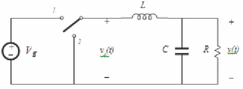
2.3 Theory of Operation Buck Converter
The buck converter, shown in Figure 2.1, converts the unregulated source voltage Vin into a lower output voltage Vout. The NPN transistor shown in Figure 1
works as a switch. The ratio of the ON time (
t
ON ) when the switch is closed to theentire switching period (T) is defined as the duty cycle D = to/T. The corresponding
PWM signal is shown in Figure 2.2 [10].
Figure 2.1: Buck Converter Circuit
Figure 2.2: PWM signal to control the switches in the
DC-DC converter
Figure 2.3: Equivalent circuit of the buck converter
when the switch is closed
Figure 2.4: Equivalent circuit of the buck converter
when the switch is open
A buck converter is a step-down DC to DC converter. Its design is similar to the step-up boost converter, and like the boost converter it is a switched-mode power supply that uses two switches (a transistor and a diode), an inductor and a capacitor.
The buck converter reducing the dc voltage, using only nondissipative switches, inductors, and capacitors. The switch produces a rectangular waveform vs(t)
as illustrated in Figure 2.5. The voltage vs(t) is equal to the dc input voltage Vg when
the switch is in position 1, and is equal to zero when the switch is in position 2. In practice, the switch is realized using power semiconductor devices, such as transistors and diodes, which are controlled to turn on and off as required to perform the function of the ideal equal to the inverse of the switching period Ts,
position 1, and is a number between zero and one. The complement of the duty ratio, D’, is defined as (1-D) [2].
Figure 2.5: Ideal switch, (a) used to reduce the voltage dc component
Figure 2. 6:(b) its output voltage waveform vs(t).
The switch reduces the dc component of the voltage: the switch output voltage vs(t) has a dc component which is less than the converter dc input voltage
Vg. From Fourier analysis, we know that the dc component of vs(t) is given by its
average value <vs>, or
(2.1)
(2.2)
So the average value, or dc component, of vs(t) is equal to the duty cycle
times the dc input voltage Vg. The switch reduces the dc voltage by a factor of D.
Figure 2 . 7: Output voltage dc component by the switching period.
What remains is to insert a low-pass filter as shown in Figure 2.7. The filter is designed to pass the dc component of vs(t), but to reject the components of
vs(t) at the switching frequency and its harmonics. The output voltage v(t) is then
essentially equal to the dc component of vs(t):
(2.3)
voltage levels using a lossless network.
The network of Figure 2.8 also allows control of the output. Figure 2.9 is the control characteristic of the converter. The output voltage, given by equation (2.3), is plotted vs. duty cycle. The buck converter has a linear control characteristic. Also, the
output voltage is less than or equal to the input voltage, since 0≤D≤1. Feedback systems are often constructed which adjust the duty cycle D to regulate the converter output voltage. Inverters or power amplifiers can also be built, in which the duty cycle varies slowly with time and the output voltage follows [3].
Figure 2 . 8 : Insertion of low-pass filter, to remove switching harmonics and pass only the dc component of vs(t) to the output.
Figure 2 . 9: Buck converter dc output the voltage V vs. duty cycle D.
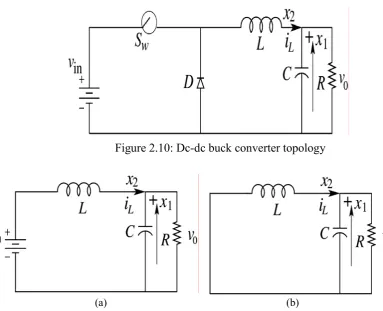
2.4 The dc-dc Buck Converter
The buck converter circuit converts a higher dc input voltage to lower dc output voltage. The basic buck dc-dc converter topology is shown in figure. 2.10. It consists of a controlled switch Sw , an uncontrolled switch D (diode), an inductor L ,
[image:24.595.210.453.322.411.2]Figure 2.10: Dc-dc buck converter topology
[image:25.595.99.506.208.368.2](a) (b)
Figure 2.11: Buck converter circuit when switch: (a) turns on (b) turns off
In the description of converter operation, it is assumed that all the components are ideal and also the converter operates in CCM. In CCM operation, the inductor current flows continuously over one switching period. The switch is either on or off according to the switching function q and this results in two circuit states. The first sub-circuit state is when the switch is turned on, diode is reverse biased and inductor current flows through the switch, which can be shown in figure 2.11(a). The second sub-circuit state is when the switch is turned off and current freewheels through the diode, which is shown figure 2.11(b).
When the switch S1 is on and D is reverse biased, the dynamics of
inductor current iL and the capacitor voltage Vc are
1
vin v0
dvC 1
iC
1
v0 dvC 1i
C
diL
dt L and
dv0
dt dt C (2.4)
When the switch S1 is off and D is forward biased, the dynamics of the circuit are
diL
dt L and
dv0
When switch S1 is off and D is also not conducting,
0 dvC 1i
C
diL
A1x + B1 A2 x + B2
1 1
0 -
RC C 0
1 , B
, B1 2
0
- 1 0 L
L
Vin 0
dt and
dv0
dt dt C (2.6)
The state space representation for converter circuit configuration can be expressed as
dx U; when S is closed,
dt U; when S is opened. (2.7)
T
x = [x1 x2 ] iL ] T
where = [vC is the state vector and A‟s and B‟s are the system matrices.
The state matrices and the input vectors for the ON and OFF periods are
A1 =A2
and U
2.5 Modes of Operation
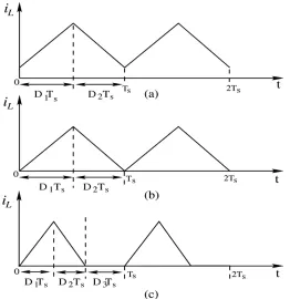
The operation of dc-dc converters can be classified by the continuity of inductor current flow. So dc-dc converter has two different modes of operation that are (a) Continuous conduction mode (CCM) and (b) Discontinuous conduction mode (DCM). A converter can be design in any mode of operation according to the requirement.
2.5.1 Continuous Conduction Mode
2.5.2 Discontinuous Conduction Mode
[image:28.612.191.453.262.532.2]When the inductor current has an interval of time staying at zero with no charge and discharge then it is said to be working in Discontinuous Conduction Mode (DCM) operation and the waveform of inductor current is illustrated in figure 2.12(c). At lighter load currents, converter operates in DCM. The regulated output voltage in DCM does not have a linear relationship with the input voltage as in CCM.
Figure 2.12: Inductor current waveform of PWM converter (a) CCM (b) boundary of CCM and DCM (c) DCM
2.6 Critical Component Values
Using this knowledge yields the following:
L.period L.closed + L.open 0 (2.8)
Substituting equations (2.4) and (2.8) into (2.9) and solving for D yields:
D Vout (2.9) Vin
Now the average inductor current equals the average of the minimum and maximum inductor current values, so the maximum inductor can be found using equation (2.11) nothing that either ΔiL,closed or ΔiL,open can be used.
ILmax = IL + (2.10)
2
Using the rule known as amp-second balance, which states the average current through a capacitor at steady state must equal zero, the average inductor current must equal the average output current.
IL = I out = Vout (2.11)
R
Substituting equations (2.8) and (2.12) into (2.11) and simplifying yields:
ILmax = Vout .
The minimum inductor current can be found in the same manner as the maximum inductor current:
ILmin = IL (2.12)
ILmin = Vout . (2.13)
The minimum inductor current is an important value, because as mentioned previously, it determines the mode of conduction. Since all previous equations were derived using the assumption of CCM, for them to remain valid iLmin can never go below zero. So by setting equation (2.15) equal to zero and rearranging to solve for L, the minimum inductor value can be found to keep the converter in CCM:
Lmin = (2.14)
Once the inductor value is determined, the minimum capacitance to maintain the desired output ripple voltage can be found. This can be done by finding how much charge is supplied by the capacitor when the switch is on or off. By using amp-second balance the average current through a capacitor must equal zero if the circuit is in steady state.
Then by calculating the area under the current wave form either when the switch is on or off will yield the change in charge. Since the current wave form is triangular the area can be found by using the formula one half times the triangle’s base times the triangles height. Where the height equals the change in current divided by two, and the base is the switching period divided by two.
Substituting equation (2.8) into (2.17) and simplifying yields:
= Vout . (2.15)
C = Δ Q .
Δ Vout
Substituting equation (2.18) into equation (2.19) yields the equation for selecting the minimum output capacitor for the desired output ripple voltage.
( 2.20) Cmin = 1 – D .V (2.17)
8.L. Δ Vout .f
2.6.1 Inductor Calculation
The minimum inductor value to keep the converter operating in continuous conduction mode down to 10% of full load is calculated by finding the output resistance that represents this load and inserting into equation (2.16).
P10% = 0.10 . Pout = 0.10 . 150 W = 15W
R10% = Vout2 = (12V)2 = 9.6W
P10% 15W
Lmin = (1-D) . R = (1-0.348).9.6Ω = 31.3μH
2.f 2.100kHz
A 56µH inductor was selected for L, since it is a standard value and 1.8 times larger than the calculated Lmin value. By substituting L and R10% into equations (2.13) and (2.15) the minimum and maximum inductor current values are calculated.
iLmin = 12 V .
iLmax = 12 V .
The difference between the maximum and minimum inductor current equals the inductor’s ripple current.
ΔiL iL max iL min (2.18)
Inserting the maximum and minimum inductor current values into equation yields:
ΔiL 1.949 A 0.551A 1.398A
2.6.2 Capacitor Calculation
Using the output ripple voltage found in table 1.2, and the value of the inductor found in section 2.2.2, the minimum output capacitance can be found using equation
2.7 Artificial Neural Network (ANN)
The term neural network was traditionally used to refer to a network or circuit of biological neurons. The modern usage of the term often refers to artificial neural networks, which are composed of artificial neurons or nodes. Thus the term has two distinct usages. There are biological neural networks and artificial neural networks. Biological neural networks are made up of real biological neurons that are connected or functionally related in a nervous system. In the field of neuroscience, they are often identified as groups of neurons that perform a specific physiological function in laboratory analysis.
Artificial neural networks are composed of interconnecting artificial neurons (programming constructs that mimic the properties of biological neurons). Artificial neural networks may either be used to gain an understanding of biological neural networks, or for solving artificial intelligence problems without necessarily creating a model of a real biological system. The real, biological nervous system is highly complex: artificial neural network algorithms attempt to abstract this complexity and focus on what may hypothetically matter most from an information processing point of view.
Good performance (e.g. as measured by good predictive ability, low generalization error), or performance mimicking animal or human error patterns, can then be used as one source of evidence towards supporting the hypothesis that the abstraction really captured something important from the point of view of information processing in the brain. Another incentive for these abstractions is to reduce the amount of computation required to simulate artificial neural networks, so as to allow one to experiment with larger networks and train them on larger data sets.
Figure 2.13. A perceptron network with three layer
Input Layer is a vector of predictor variable values (x1...xp) is presented to the input layer. The input layer (or processing before the input layer) standardizes these values so that the range of each variable is -1 to 1. The input layer distributes the values to each of the neurons in the hidden layer. In addition to the predictor variables, there is a constant input of 1.0, called the bias that is fed to each of the hidden layers; the bias is multiplied by a weight and added to the sum going into the neuron [1].
Hidden Layer is a arriving at a neuron in the hidden layer, the value from each input neuron is multiplied by a weight (wji), and the resulting weighted values are added together producing a combined value uj. The weighted sum (uj) is fed into a transfer function, σ, which outputs a value hj. The outputs from the hidden layer are distributed to the output layer.
Output Layer is a arriving at a neuron in the output layer, the value from each hidden layer neuron is multiplied by a weight (wkj), and the resulting weighted values are added together producing a combined value vj. The weighted sum (vj) is fed into a transfer function, σ, which outputs a value yk. The y values are the outputs of the network.
CHAPTER 3
METHODOLOGY
3.1 Research Design
The proposed general block diagram for Voltage tracking of Buck converter using Neural Network Controller (NNC) is shown in Figure 3.1. The operation of this circuit consists buck converter and neural network circuit (NNC). The source for this circuit is dc input and reference voltage Vref. The output for step down buck converter is controlled by Neural Network Control (ANN) and feedback element for the error automatically process to the summing point.
Figure 3.1: Block diagram of the proposed NNC of Buck Converter
3.2 Mathematical Modeling of Buck Converter
3.2.1 State-Space Representations
The buck converter is nonlinear, time-dependent system and its operation is described by the two modes, illustrated in Figure 12 (a) and (b). The system is linearized through switch averaging method about a selected operating point, and with respect to the transistor duty cycle, k.
Figure 3.2 : a) Mode 1 (b) Mode 2
Mode 1 of operation is described by two differential equations derived from the circuit in Figure 3.2 (a) and consistent with transistor Q switch being turn on:
(3.1) (3.2)
The state-space representation for mode 1 (transistor is on) is given by:
(3.3)
(3.4)
[1] W.M.Utomo, T Taufik, R.Heriansyah “Online Learning Neural
Network Control of Buck Boost Converter”, 8t h International Conference
on Information Technology: New Generations, 2011 ,pp 485-489
[2] Y. S. Lee, Computer-Aided Analysis and Design of Switch-Mode Power Supplies, Marcel Dekker, Inc., New York, Basel, Hong Kong, 1993.
[3] J. Arias, A. Arias, S. Gomariz and F. Guinjoan, “Generating design rules for buck converter-based fuzzy controllers”, 1996 IEEE International Symposium on Circuits and Systems, Vol. 1, pp. 585 – 588, May 1996.
[4] T. Gupta, R. R. Boudreaux, R. M. Nelms and J. Y. Hung, “Implementation of a Fuzzy Controller for DC-DC Converters Using an Inexpensive 8-b Microcontroller”, IEEE Trans on Industrial Electronics, Vol. 44. pp. 661-669, October 1997.
[5] Y. Shi and P. C. Sen, “Application of Variable Sturcture Fuzzy Logic Controller for
DC-DC Converters”, The 27th Annual conference of the IEEE Industrial Electronics Society, pp. 2026-2031, Nov 2001.
[6] Mohan, Underland, Robbins “Power Electronics converters applications and design” John Wiley & sons, inc. 2003 pp- 231-303.
[7] A. Perry, G. Feng, Y. Liu and P. C. Sen, “A new design method for PI-like fuzzy
logic controllers for DC-DC converters”, 35th Annual IEEE Power Electronics Specialists Conference, Aachen, Germany, pp. 3751-3757, 2004.
[8] M. Ahmed, M. Kuisma, K. Tolsa and P. Silventoinen, “Implementing Sliding Mode
[9] L. Guo, J. Y. Hung, and R. M. Nelms, “PID controller modifications to improve steady-state performance of digital controllers for buck and boost converters”, Conference Proceedings of IEEE Applied Power Electronics Conference and Exposition, pp. 381 – 388, Feb 2002.
[10] Jean Paulo Rodrigues, Samir Ahmad Musa, “Three-Level ZVS Active Clamping PWM fo the DC-DC Buck Converter”, IEEE Transaction On Power Electronic, Vol 24, pp. 2249-2257, Oct 2009
[11] Xiong Du, Luowei Zhou, “Double Frequency Buck Converter”, IEEE Transactions On Industrial Electronic, Vol 56, pp 1690-1698, May 2009
[12] L.Premalatha, P.Vanajaranjan “Spectral Analysis of DC-DC Buck Converter with Chatic Dynamics”, IEEE Indicon Conference Chennai India, pp. 605-608, Dec 2005
[13] F. H. Wang and C. Q. Lee, “Comparison of Fuzzy Logic and Current-Mode Control
Techniques in Buck, Boost and Buck/Boost Converters”, 1995 IEEE 26th Annual Power Electronics Specialists Conference, Vol. 2, pp. 1079 – 1085, June 1995.
[14] Su, J.H.; Chen, J.J.; Wu, D.S.; “Learning feedback controller design of switching
converters via Matlab/Simulink” Education, IEEE Transactions on, Volume: 45
Issue: 4, Nov. 2002 Page(s): 307 -315
[15] Huang, W.; A new control for multi-phase Buck converter with fast transient
response, ON Semiconductor (2001).
Fuzzy Controller for DC-DC Converters Using an Inexpensive 8-b Microcontroller”, IEEE Trans on Industrial Electronics, Vol. 44. pp. 661-669, October 1997.
[18] W. C. So, C. K. Tse and Y. S. Lee, “Development of a Fuzzy Logic Controller for DC/DC Converters: Design, Computer Simulation, and Experimental Evaluation”, IEEE Transaction on Power Electronics, Vol. 11. pp. 24-32, January 1996.
[19] M. Smyej, M. Saneba and A. Cheriti, “A Fuzzy Controller for a DC to DC Converter Using a Digital Integrator”, Canadian Conference on Electrical and Computer Engineering, Vol. 1, pp. 7-10, 2000.
[20] J. Y. Hung, W. Gao and J. C. Hung, “Variable Structure Control: A Survey”, IEEE Transaction on Industrial Electronics, Vol. 40, No. 1, pp. 2-22, Feb 1993.
[21] J. Mahdavi, A. Emadi and H. A. Toliyat, “Application of State Space Averaging
Method to Sliding Mode Control of PWM DC/DC Converters”, 32nd IEEE Industry Applications Society Annual Meeting, pp. 820-827, Oct 1997.
[22] D. Cortes, J. Alvarez and J. Alvarez, “Robust Sliding Mode Control for the Boost Converter”, VIII IEEE International Power Electronics Congress, pp. 208-212, Oct 2002.
[23] E. Vidal-Idiarte, L. Martinez-Salamero, F. Guinjoan, J. Calvente and S. Gomariz, “Sliding and Fuzzy Control of a Boost Converter using an 8-bit Microcontroller”, IEE Proceedings of Electric Power Applications, Vol. 151, pp. 5-11, Jan 2004.
[24] R. Orosco, N. Vazquez, “Discrete Sliding Mode Control for DC/DC Converters”, VII IEEE International Power Electronics Congress, pp. 231-236, Oct 2000.
[25] Y. Shi and P. C. Sen, “Application of Variable Sturcture Fuzzy Logic Controller for
[26] M. Ahmed, M. Kuisma, K. Tolsa and P. Silventoinen, “Implementing Sliding Mode
Control for Buck Converter”, 2003 IEEE 34th Annual Power Electronics Specialist Conference, Vol. 2, pp. 634-637, June 2003.
[27] G. Venkataramanan and D. Divan, “Discrete Time Integral Sliding Mode Control for
Discrete Pulse Modulated Converters”, 21st Annual IEEE Power Electronics Specialist Conference, pp. 67-73, June 1990.
[28] Q. Hu, Z. Liang, H, Yu, G. Xia and X. Yang, “Application of Sliding Mode Control in Control of Power Electronic Converters”, Proceedings of the Fifth International Conference on Electrical Machines and Systems, Vol. 1, pp. 608-611, Aug 2001.
[29] W. Gao, Y. Wang and A. Homaifa, “Discrete-Time Variable Structure Control Systems”, IEEE Transactions on Industrial Electronics, Vol. 42, No. 2, pp. 117 – 122, April 1995.
[30] J. Matas, L. G. Vicuna, O. Lopez, M. Lopez and M. Castilla, “Discrete Sliding Mode
Control of a Boost Converter for Output Voltage Tracking”, 8th International Conference on Power Electronics and Variable Speed Drives, pp. 351-354, Sep 2000.