Modeling, Simulation and Optimization of High
Performance CIGS Solar Cell
Mahmud Abdul Matin
Bhuiyan
Chittagong University of Engineering and Technology
Dept. of Electrical and Electronic Engineering
Mohammad Shafkat Islam
Chittagong University of Engineering and Technology
Dept. of Electrical and Electronic Engineering
Amit Jyoti Datta
Chittagong University of Engineering and Technology
Dept. of Electrical and Electronic Engineering
ABSTRACT
Numerical Modeling, Simulation and Optimization of High Performance three layers CIGS Solar cell have been carried out in this paper using AMPS-1D (Analysis for Microelectronic and Photonic Structures). CIGS thin film hetero-junction solar cell simulation is performed to find out the influence of particular layer material electrical, optical and geometric parameters on overall cell performance. Based on the simulation results, Optimization is performed by choosing the optimum value of all input parameters from observation of overall cell performance over wide range of individual input parameter variation. The values for input parameters of three layers are chosen from literature values, theoretical values and numerical data. Current tested maximum CIGS solar cell efficiency is 20.3%. This proposed model provides simulated efficiency of 21.613% from simulation by AMPS-1D software in LIFETIME model while lifetime is approximated 1ns.
General Terms
Numerical Modeling, Simulation and Optimization.
Keywords
Cu(In,Ga)Se2 (CIGS), thin film solar cell, AMPS-1D
simulation, Efficiency, open circuit voltage (Voc), short circuit
current (Jsc), fill factor(FF)
1. INTRODUCTION
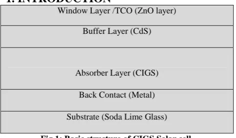
Window Layer /TCO (ZnO layer)
Buffer Layer (CdS)
Absorber Layer (CIGS)
Back Contact (Metal)
[image:1.595.48.290.518.659.2]Substrate (Soda Lime Glass)
Fig 1: Basic structure of CIGS Solar cell
Light strikes the solar cell on ZnO layer which is known as the window layer or transparent conducting oxide layer (TCO). The material to be used as TCO layer must satisfy two requirements- a) the bandgap of TCO layer should be high enough to ensure absorption of maximum amount of incident sunlight and b) TCO must remain transparent for most of the solar spectrum so that maximum photons can be effectively absorbed [1]. Since ZnO is cheap and easy to grow, so it is the general choice. Reflection from the window layer, TCO is
responsible for reduction in solar cell efficiency. So, the top of the cell must be deposited with anti-reflection coating to keep reflection losses within reasonable limits. ZnO layer has typical thickness of 0.3-0.4 µm.
A buffer layer is introduced in between the p-type CIGS absorber and TCO layer because experiments show superior performance of cell with a buffer layer compared with a cell without it. CdS is used as a buffer layer. CdS is a direct bandgap semiconductor with bandgap of 2.4 eV. Devices with alternative buffer layer provide inferior performance compared with CdS [2]. Buffer layer provides several advantages including lower interface recombination and reduces damage due to sputtering of ZnO layer on CIGS [3]. It also reduces reflection losses in the front surface because it has refractive index which is comparable with ZnO and CIGS. CdS is n-type material which forms p-n junction with p-type CIGS. The thickness of CdS is chosen as trade-off between losses due to absorption by CdS and beneficial effects. Optimum thickness lies around 50-100nm.
CIGS is used as the absorber layer which is the most important layer in the PV device. Cu (In,Ga)Se2 is a
compound semiconductor exhibiting chalcopyrite crystal structure having large absorption coefficient (α~105
cm-1) [1]. CIGS is formed by partial substitution of In by group III element Ga. The band-gap can be changed by changing x in CuIn1-xGaxSe2. Absorber p-type CIGS has large concentration
of holes and n-type CdS has large concentration electrons. Excess electron hole pairs are generated by the light that is absorbed by the CIGS layer. Asymmetric nature of hetero-junction causes hole to flow towards the underlying back contact and electron to flow towards the upper layer, CdS. It results in a net current flow in the illuminated hetero-junction.
Back contact performs the function of collecting carriers from the absorber and delivering it to an external load. CIGS solar cells having Mo back contact gives superior performance compared with other metals [1]. Molybdenum allows diffusion of Na from substrate to the absorber which increases cell efficiency. Metals to be used as back contact must have low resistivity and should not hinder the flow of majority carriers and holes. Back contact is also defined by its work function and reflectivity at the contact-semiconductor interface.
2. SIMULATION
The optimum high performance CIGS solar cell is determined from following steps-
1. Absorber Layer, CIGS Optimization 2. Buffer Layer, CdS Optimization 3. Back Contact Change
[image:2.595.315.542.94.349.2]The material properties and absorption spectrum for ZnO, CIGS and CdS have been taken from [5].
Table 1. Material properties for basic CIGS materials [5]
Layer Properties ZnO CdS CIGS
Width [nm] 50 50 3000
Dielectric constant [ε/ε0]
9.0 10.0 13.6
Electron mobility, µe[cm2 /Vs]
100 100 100
Hole mobility, µh
[cm2 /Vs]
25 25 25
Carrier density
[cm-3]
ND = 1018 ND= 1017 NA=2x10¹⁶
Bandgap, Eg [eV] 3.3 2.4 1.12
Effective dens. NC [cm-3]
2.22x10¹⁸ 2.22x10¹⁸ 2.22x10¹⁸
Effective dens. NV [cm-3]
1.78x10¹⁹ 1.78x10¹⁹ 1.78x10¹⁹
Electron affinity [eV] 4.0 3.8 4.1
2.1 Absorber Layer CIGS Optimization
CIGS Layer optimization is done from following steps- 1. Change in band-gap of CIGS to find out most efficient band-gap.
2. Changing thickness to determine optimum thickness for absorber layer.
3. Effect of carrier density (NA) on cell performance. 4. Electron mobility (MUN) change.
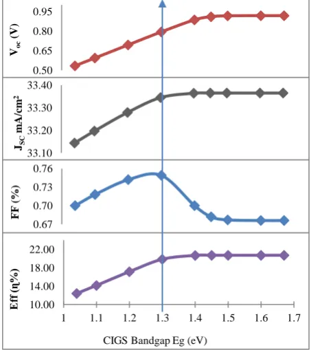
2.1.1 CIGS Bandgap Change
The bandgap of CIGS absorber layer was varied keeping all other parameters of the base case fixed. The thickness of CIGS layer was fixed to 3000nm. Bandgap was varied from 1.04 to 1.67eV according to equation 2.1 from [6].
E(x) =1.02 +0.67x+0.11x(x-1) (2.1) From simulation it is found that as the bandgap increases, Voc
increases with it, as expected [7]. Jsc has negligible change.
So, ultimately Efficiency increases. But Fill factor decreases sharply after 1.3 eV because increased Ga content causes defects; electron and hole affinities are affected. Maximum efficiency obtained close to 1.5eV which supports the Shcokley-Quisser Limit theory [8]. AMPS 1-D is used for simulation. A description of both modes of AMPS can be found from [9].
1.5 eV is chosen as the optimum bandgap, because it shows 20.702% efficiency in simulation when all the other parameters are fixed on the base case and thickness of CIGS absorber layer is fixed to 3000nm. Further increase in bandgap
decreases efficiency due reduction in fill factor. Indium content is 25.26% for x=0.7474 from equation 2.1 for 1.5 eV.
Fig 2: Effect of CIGS Bandgap change on cell performance
2.1.2 CIGS Layer Thickness Change
The bandgap of CIGS is fixed to 1.5 eV and the thickness of the cell is reduced from 5000nm to reduce the high material cost due to In consumption and determine optimum thickness. The thickness is reduced from 5000nm to 500nm and performance of the cell is simulated. Results shown in Fig 3
[image:2.595.48.291.174.462.2]
Fig 3: Effect of CIGS thickness change on cell performance
If the cell is not made thick enough, some of the energy that does not get coupled into the cell will pass straight out the back [7]. So, as the absorber is made thinner than 2500nm Voc, Jsc decreases and ultimately causes reduction in
0.50 0.65 0.80 0.95
Voc
(V)
33.10 33.20 33.30 33.40
JSC
m
A
/c
m
2
0.67 0.70 0.73 0.76
FF
(%
)
10.00 14.00 18.00 22.00
1 1.1 1.2 1.3 1.4 1.5 1.6 1.7
E
ff
(ɳ
%
)
CIGS Bandgap Eg (eV)
0.80 0.85 0.90 0.95
V
o
c
(V
)
30.00 31.00 32.00 33.00
J
sc
0.65 0.68 0.71 0.74
FF
(%
)
18.00 18.80 19.60 20.40
0 1000 2000 3000 4000 5000
E
ff
(ɳ
%
)
[image:2.595.316.542.455.684.2]Efficiency. Fill factor decreases with thicker absorber because of bulk resistance of the semiconductor. The overall efficiency of the cell increased with thickness because of the combined effect of Voc and Jsc dominate the decrease of Fill factor.
2500nm is chosen to be optimum thickness because it results in maximum efficiency of 20.707% when bandgap is fixed to 1.5 eV. Further increase in thickness reduces the overall efficiency by small amount because decrease in fill factor dominates the small increase in Voc and Jsc.
2.1.3 CIGS Carrier Density (NA) Change
The carrier density, NA in the CIGS absorber can be determined from capacitance voltage measurements [5]. The changes induced by NA can be described by diode equations-
(2.2)
(2.3)
From eq (2.3) increasing NA increases the denominator of IO,
hence lowers the saturation current, IO. Since denominator of
eq (2.2) decreases so Voc increases with increase in NA.
[image:3.595.316.543.97.396.2]Based on the range of carrier density of CIGS obtained from [5], performance of the cell is simulated from NA=1015 to 3x10¹⁷ using AMPS-1D and the results are given below
Fig 4: CIGS Carrier Density change
From Fig 4, the optimum NA is chosen to be 4x1016 cm-3.
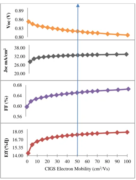
2.1.4 CIGS Electron Mobility Change
Mobilities for typical CIGS is taken as µe = 100 cm 2
/Vs, one third mono-crystalline material, due to grain boundary effects
[5]. (2.4)
When mobility increases the diffusion coefficient De increases
with it. The increase in De causes reduction in Voc and
increase in Io according to eq (2.2) and (2.3). Therefore, an
increase in electron mobility µe increases I0 and lowers
Voc.The mobility of CIGS layer is varied within 0-100
cm2/Vs.
Fig 5: CIGS Electron mobility change
2.2 Buffer Layer CdS Optimization
After determining optimum parameters for absorber layer, the buffer layer was optimized following the steps-
1. Thickness change of Buffer layer, CdS 2. CdS Hole mobility change
3. CdS Carrier density (ND) change
From the simulated results for CdS thickness change, overall efficiency decreases with increase in thickness above 100nm due to bulk resistance in Buffer layer. 100 nm is chosen to be the optimum thickness for CdS because it is comparatively easier to manufacture than ultra thin CdS of 50nm thickness and it provides maximum efficiency.
The simulation of hole mobility from 0-100cm2/Vs shows that Voc remains constant over the entire range of mobility
variation. Jsc and Fill factor increase by small amount with
increase in hole mobility. Therefore efficiency increases by very small amount approximately 0.2% with increase in mobility from 0 to 100. Optimum hole mobility is fixed from the simulation to 50 cm2/Vs.
Default value of CdS carrier density, ND is 1017 cm-3 [5]. The effect of ND is simulated by changing ND from 0- 3x1017cm-3
using AMPS-1D.Within 0 to default value 1017 cm-3 range, Voc
decreases with increasing ND and Jsc increases with increase
in ND. So Efficiency increases until default value. Above 1017cm-3 efficiency increases by extremely small. Increase beyond 1017 cm-3 decreases Fill factor. Therefore, 1017 cm-3 is the optimum value of ND for CdS.
0.50 0.65 0.80 0.95
V
o
c
(V
)
26.00 28.30 30.60 32.90
J
sc
0.25 0.40 0.55 0.70
FF
(%)
7.00 10.60 14.20 17.80
1.00E+15 1.01E+17 2.01E+17 3.01E+17
E
ff
(
η
%)
CIGS Carrier density (cm-3)
0.80 0.83 0.86 0.89
V
o
c
(V
)
20.00 26.00 32.00 38.00
J
sc
m
A
/c
m
2
0.56 0.60 0.64 0.68
FF
(%
)
14.00 15.35 16.70 18.05
0 10 20 30 40 50 60 70 80 90 100
E
ff
(%
Ƞ)
[image:3.595.54.282.300.600.2]2.3 Effect of Back Contact on Cell
Performance
ϕBL and Back contact reflectivity is varied to observe the
effect on cell performance.
2.3.1 Effect of Changing ϕ
BLof Back Contact
The effect of changing the back contact of CIGS solar cell on cell performance is simulated changing ϕBL within 0.5-1.3eV(Fig 6). Voc, Jsc and fill factor all three parameters increase with Back contact ϕBL. Therefore, the cell efficiency
increases. 0.9 eV ϕBL Molybdenum back contact is chosen as
the optimum back contact for CIGS solar cells.
Fig 6: Effect of back contact ϕBL change
2.3.2 Effect of Back Contact Reflectivity on Cell
Performance
The results of simulation show very small increase in Jsc and
Fill factor with increase in back surface reflectivity. So, Efficiency is affected by small amount. Final optimum solar cell is selected keeping reflectivity at 0.9. So, simulation supports the theory that back surface reflection has negligible effect on solar cell performance
3. RESULT
[image:4.595.316.547.80.212.2]The I-V curve of Final CIGS solar cell is shown in Fig 7. The variation of the performance of the final high performance CIGS solar cell with operating temperature is shown below in Fig 8.
Fig 8: Normalised Voc and Efficiency as a function of temperature
Voc and Fill factor decrease with operating temperature
because bandgap slightly decreases with temperature, and Jsc increases with increase in bandgap.So, ultimately efficiency decreases with increase in operating temperature.
4. CONCLUSION
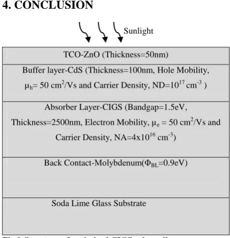
Sunlight
TCO-ZnO (Thickness=50nm)
Buffer layer-CdS (Thickness=100nm, Hole Mobility,
µh= 50 cm2/Vs and Carrier Density, ND=1017 cm-3 )
Absorber Layer-CIGS (Bandgap=1.5eV,
Thickness=2500nm, Electron Mobility, µe = 50 cm2/Vs and
Carrier Density, NA=4x1016 cm-3)
Back Contact-Molybdenum(ΦBL=0.9eV)
[image:4.595.55.284.237.472.2]Soda Lime Glass Substrate
Fig 9:Structure of optimized CIGS solar cell
Final simulated high performance CIGS solar cell has Voc=0.905 Volts, Jsc=34.106 mA/cm2 and Fill factor 0.7. The efficiency of the final cell at 298 K is 21.613%.
Table 2. Comparison of performance parameters of simulated baseline case from [10] and proposed model.
3.1 I-V Curve of final CIGS Solar cell
Fig 7: I-V Curve of Final High Performance CIGS Cell
Performance Parameter
Baseline CIGS Proposed Model
Open Circuit Voltage, Voc
0.64 Volts 0.905 Volts
Short Circuit Current, Jsc
34.6 mA/cm2 34.106 mA/cm2
Fill Factor 0.795 0.7
Efficiency 17.7 % 21.613%
0.45 0.60 0.75 0.90
V
o
c
(
V
)
33.2 33.3 33.5 33.6
J
sc
0.50 0.60 0.70 0.80
FF
(%
)
8.50 14.50 20.50 26.50
0.5 0.6 0.7 0.8 0.9 1 1.1 1.2 1.3
Ef
f (
%
ɳ)
Back contact (φBL)
0.84 0.88 0.92 0.96 1
10 20 30 40 50 60 70 80 90 100
N
o
rm
a
li
sed
ɳ
a
n
d
V
o
c
(%
)
Temperature (°C)
Normalised Voc Normalised Efficiency
0 20 40
0 0.2 0.4 0.6 0.8 1
Jsc
(mA
/c
m
2)
[image:4.595.313.549.292.536.2] [image:4.595.54.275.651.751.2]One of the major problems of solar cell is high price. In CIGS solar cell the main problem lies in high price and scarcity of In. The results obtained from simulation shows that partial replacement of In from ideal CIS to form CIGS would result in increase in superior performance because of increased bandgap lies within the optimum 1.5 eV range predicted by Shockley–Queisser limit. The results obtained also show that if back contact ϕBL can be increased the efficiency of the cell
improves significantly. Current research is being done on reducing back contact recombination and band gap grading to reduce losses in the back contact and improve cell performance .
5. ACKNOWLEDGMENTS
We would like to thank all the teachers of the Department of EEE, CUET.
6. REFERENCES
[1] Ana Kanevce, 2007. Anticipated performance of Cu(In,Ga)Se2 solar cell in the thin-film limit.
[2] Alexei O. Pudov, 2005. Impact of secondary barriers on CuIn1−xGaxSe2 solar cell operation.
[3] A. Ennaoui, W. Eisele, M. Ch. Lex-Steiner, W. Riedl, and F. Karg. 2000. Cd-free Cu(Ga,In)(SSe)2 Thin Film
Solar Cells and Mini modules. In 16th European Photovoltaic Sol. Energy Conf., pages 682–685.
[4] Shirish Pethe, 2004. Optimization of the two stage process for Cu(In,Ga)Seâ solar cells
[5] Markus Gloeckler, 2003. Numerical Modeling of CIGS Solar Cells: Definition of the Baseline and Explanation of Superposition Failure. Colorado State University, Fort Collins, Colorado.
[6] M. Gloeckler, A.L. Fahrenbruch, and J.R. Sites Numerical Modeling of CIGS and CdTe Solar cells: Setting the Baseline.
[7] Martin A.Green,, Solar Cells - Operating Principles Technology and Systems Applications, Prentice Hall Inc.
[8] William Shockley and Hans J. Queisser, "Detailed Balance Limit of Efficiency of p-n Junction Solar Cells", Journal of Applied Physics, Volume 32 (March 1961).
[9] S. Fonash, "A Manual for AMPS-1D for Windows 95/NT", The Pennsylvania State University, 1997.
[10] M. Gloeckler, 2005. Device physics of Cu(In,Ga)Se2
thin-film solar cell. Doctoral thesis.