Conditional Precharge Dynamic Buffer Circuit
Amit Kumar Pandey
Department of Electronics and Communication Engineering,
M.N.N.I.T, India.
Vivek Mishra
Department of Electronics and Communication Engineering,
M.N.N.I.T, India.
Ram Awadh Mishra
Department of Electronics and Communication Engineering,
M.N.N.I.T, India
Rajendra Kumar Nagaria
Department of Electronics and Communication Engineering, M.N.N.I.T, India.
V. Krishna Rao Kandanvli
Department of Electronics and Communication Engineering, M.N.N.I.T, India.
.
ABSTRACT
In this paper, footless domino logic buffer circuit is proposed. It minimizes redundant switching at the dynamic and the output nodes. This circuit passes propagation of precharge pulse to the dynamic node and avoids precharge pulse to the output node which saves power consumption. Simulation is done using 0.18µm CMOS technology. We have calculated the power consumption, delay and power delay product of proposed circuit and compared the results with existing circuits for different logic function, loading condition, clock frequency, temperature and power supply. For capacitance 500fF, our proposed circuit reduces power consumption by 72.69%, 26.35% and 24.03% as compared to standard footless domino, SP-Domino and SSPD techniques.
Keywords
Buffer, Domino circuit, Power consumption, Delay, Precharge pulse.
1.
INTRODUCTION
Domino logic circuits are used in wide applications such as memory [1], microprocessor [2], adder [3] etc. It has superior advantage over static logic circuit, it require less area and reduces output load capacitance hence enhance the speed. Realization of wide fan-in gates using static logic circuit requires long stack of pMOS and nMOS which is not practical, it increase the delay and area. But domino logic use dual phase namely precharge and evaluation to implement complex circuit with single evaluation network [4].Domino circuit has drawback of high power consumption due to clock loading and reduce noise margin due to charge sharing and charge leakage. Charge sharing and charge leakage is compensated by adding keeper transistor.
Buffer is essential to drive the output of domino circuit into the next stage [5]. Static CMOS logic circuit consumes power during the toggling of the output state. Domino logic circuit consumes power due to the unwanted redundant switching at dynamic and output nodes. This redundant switching of domino logic circuit consumes more power as compared to static CMOS circuit. Different circuits are proposed in the literature to deal this issue. Single phase domino logic [6] and static switching pulse domino [7] logic reduces the redundant switching at both dynamic and output node. True single phase clock domino logic (TSPC) [8], [9], limited switch dynamic logic (LSDL) [10] and pseudo dynamic buffer (PDB) [11] reduces the redundant switching only at output node
.
Power dissipation of the domino circuit is divided into three components [5]:
(1)
PDynamic is the power consumed during capacitance charging
and discharging, PLeakage is the total leakage power of the
circuit and this power increases as the technology is scaled down, and PShort Circuit is the power dissipated when direct
current flows from power supply to ground.
(2)
Where is the redundant switching at the output and dynamic node, it depends on the gate topology and inputs, C is the capacitive load at the evaluation node, Fclk is the clock frequency.
(3)
Where ILeakage is the combination of subthreshold and gate oxide leakage current.
(4)
ISC for domino logic gate is the contention current that flows between the evaluation network and pMOS keeper during evaluation mode. This power dissipation must be kept low for better operation of the domino circuit.
In this paper, we propose switching-aware technique which minimizes redundant switching at the dynamic and output nodes, and the circuit behaves like static CMOS circuits. Pull up network consist of combination of a PMOS and NMOS transistor. Dynamic node is conditional precharge to high voltage only when both the transistors of pull up network turns ON and the pull down network turns OFF simultaneously at the start of each clock high for short duration of time. Using this technique, it allows the propagation of precharge pulse to the dynamic node and avoids the precharge pulse to the output node. The remainder of the paper is organized as follows. Previous proposed techniques are described in section 2. Proposed circuit is described in section 3. Simulation results are presented in section 4, and conclusion is presented in section 5.
2.
PREVIOUS WORK
During prechrage phase, M1 turns ON, dynamic node is charged to high voltage and output is discharged to low voltage. During evaluation phase dynamic node is discharged to low voltage and output is charges to high voltage. When input is kept low, dynamic node maintain high in both operating phase. Here propagation of precharge pulse is needed at the dynamic node and prevented at the output node to make the circuit stable. This redundant switching increase the power consumption.
VDD
VDD
CLK
DYN M1
OUT
CL
M5
M3
M4 IN
VDD
M2
Figure 1. Standard footless domino circuit.
Input
Clock
Dyn
Out
Figure 2. Voltage characteristics at various node of standard footless circuit.
Circuit techniques have been proposed in the literature such as single phase SP-Domino logic, static switching domino logic. Main idea regarding these circuit designs is to reduce redundant switching at both dynamic and output nodes.
2.1
Single-Phase SP-Domino Logic
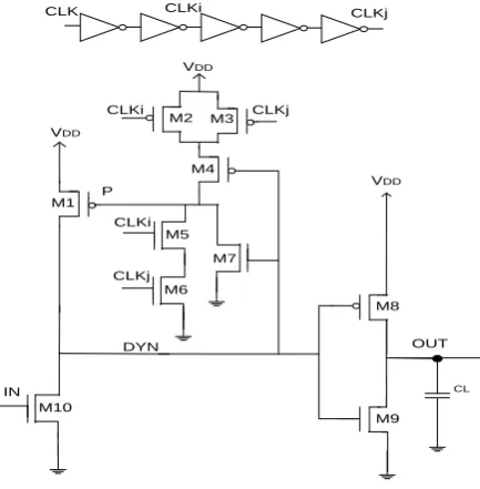
Single phase domino logic is similar to the clock delayed domino logic [13] is shown in Fig.3 and its voltage
characteristics is shown in Fig.4. The latest arriving of input does not arrive before the rising edge of the delayed clock [6]. The gate has single phase as both pull up and pull down network of the dynamic node occurs during the evaluation phase. Transistor M1 works as pull up and keeper. Pulse generator produce signal P which turns ON M1 unconditionally at the start of evaluation cycle. If both transistor M1 and M10 turns on simultaneously, small contention current flows between them for short duration of pulse P at the gate of M1.If the transistor M10 turns OFF at the start of evaluation phase, M1 charged the dynamic node to high voltage. If the value of dynamic node is low at the end of pulse signal P, M7 remains OFF and P is pulled up high by transistor M4.Charging operation of the dynamic node starts after the pulse signal returns to low voltage. The logical expression for pulse P is
(5)
Where CLKi and CLKj are clock delayed signal and its delayed inverse.
Design of SP-Domino has several flaws. Size of M1 has lack of flexibility. If the size of M1 increases, keeper ratio increases. Keeper ratio is defined as the ratio of current driving capability of transistor M1 to the transistor M10. High keeper ratio increases the contention current and the delay. High keeper ratio has unsymmetrical rise and fall time of the output signal. To have symmetric rise and fall time, K must be a fixed value.
VDD
DYN OUT
CL
M10
M8
M9 IN
VDD
M1
M5
M6 M7 M2
VDD
M3
M4
CLK CLKi CLKj
CLKi
CLKi
CLKj
CLKj P
[image:2.595.323.540.406.627.2]
CLKi
CLKj
P
Input
Dyn
[image:3.595.150.459.80.262.2]Out
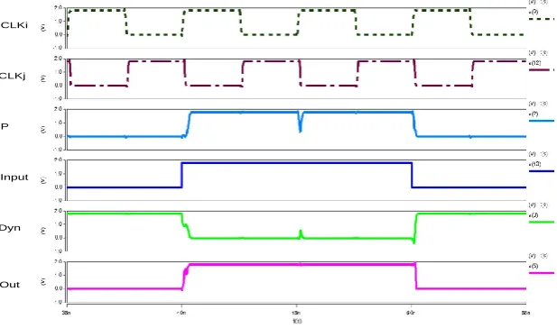
Figure 4.Voltage characteristics at various node of single phase domino logic.
VDD
VDD
DYN M1
CL
M7
M3
M4 CLK
VDD
M2
CLK CLKi
OUT
M5
M6 OUT
M8 IN
G1
G2
CCLKd
CLK A CLKi
CCLKi DYN
B
CLKi Conditional Pulse
Generator
G1 B
M9
M11
M13 M14
M15 M16
CCLKd
CLK
DYN
CCLKi
CCLKi
CLK
DYN
CCLKd CCLKd
DYN
CLK CCLKi
B
M10
M12
G2
M19 M20
DYN
DYN A
A
CLKi
CCLKd CLKi
DYN A CCLKd
M17
M18
M21
[image:3.595.93.488.318.706.2]2.2 Static switching pulse domino (SSPD)
SSPD is similar to SP-Domino with static input and output characteristics [7]. SP-Domino uses single transistor as pull up and keeper but in case of SSPD employs separate transistors M1 and M2. Both transistors M1 and M2 never ON simultaneously. SP-Domino has lack of flexibility in designing the size of transistor M1 to get symmetrical rise and fall delay of the output. SSPD allows independent tuning of rise and fall delays.
[image:4.595.325.543.99.301.2]SSPD technique employs a conditional pulse generator (CPG) is shown in Fig.5 and its voltage characteristics is shown in Fig. 6. The CPG generate pulse, M1 turns OFF only when the dynamic node has been discharged or held low in last evaluation cycle and Keeper M2 turns OFF. If the dynamic node is not discharged, M1 is OFF by CPG. M8 is ON providing contention current by the keeper.CPG internally generate two additional clock phases CCLKd and CCLKi. Their behavior is related to the clock signal (CLK) and dynamic node. The two clock phases utilized by the block G1 in CPG to produce pulse B. Drawback of this technique is that it require complex conditional pulse generator. The logical expression for pulse B is
(6)
Where CCLKd and CCLKi are the conditionally generated delayed and inverse phases of the original clock CLK
.
CLK
CCLKd
CCLKi
Input
DYN
OUT
A
[image:4.595.322.544.115.471.2]B
Figure 6. Voltage characteristics at various node of static switching pulse domino.
3.
PROPOSED WORK
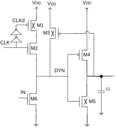
The proposed buffer circuit has static input and output characteristics, its circuit diagram as shown in Fig. 7. Voltage characteristics at different node as shown in Fig.8. Combination of PMOS M1 and NMOS M2 works as function of pull up network
and
M3 as keeper transistor. Input of M2 is clock (CLK) and M1 is non-inverting delayed clock (CLKd). Timing diagram of clocks is shown in Fig.9. Dynamic node is conditional precharge to high voltage only when both the transistors of pull up network turns ON and the M6 turns OFF simultaneously at the start of each clock high for short duration of time Td. Using this technique, it allowsthe propagation of precharge pulse to the dynamic node and avoids the precharge pulse to the output node.
VDD
VDD
DYN M1
CL
M6
M4
M5 IN
VDD
M3 CLKd
OUT M2
CLK
Figure 7. Circuit diagram of proposed circuit.
CLK
CLKd
Input
Dyn
[image:4.595.321.540.326.707.2]Out
Figure 8. Voltage characteristics at various node of proposed circuit.
CLK
CLKd
M2 ON M2 OFF M2 ON M2 OFF
M1 OFF M1 ON M1 OFF
M1 ON
Td
Both M1 and
M2 are ON
Td
[image:4.595.61.279.378.592.2]Operation of the circuit is explained by considering the input logic. During clock is low, dynamic node holds the previous value regardless of the input of the circuit.
Case 1: When input is high, at the start of clock high, for a short period of time Td, CLK is high and delayed clock CLKd is low. M1, M2 and M6 are turned ON provides contention current to the pull down network as shown in Fig.10. Size of M6 is large enough to discharge the dynamic node to low voltage. After the delay of time Td, both CLK and CLKd is high and M1 turns OFF as shown in Fig.11. Thus no further contention current flows to the pull down network and dynamic node remains at logic low.
VDD
VDD
DYN M1
M6
M4
M5 IN
VDD
M3 CLKd
M2 CLK
Contention Current
[image:5.595.323.509.92.281.2]CL
Figure 10. Operation of the proposed circuit when the input is high for short period of time delay Td.
VDD
VDD
DYN M1
CL
M6
M4
M5 IN
VDD
M3 CLKd
[image:5.595.61.251.210.409.2]M2 CLK
Figure 11. Operation of the proposed circuit when the input is high after the time delay Td.
Case 2: When input is low, at the start of clock high, CLK is high and delayed clock CLKd is low. M1 and M2 turned ON simultaneously charged the dynamic node to logic high as shown in Fig.12. For the rest of the clock high, both CLKand CLKd are high, M1 turns OFF as shown in Fig.13. Dynamic node remains at logic high.
VDD
VDD
DYN M1
CL
M6
M4
M5 IN
VDD
M3 CLKd
M2 CLK
[image:5.595.324.509.315.502.2]Charging Current
Figure 12. Operation of the proposed circuit when the input is low for short period of time delay Td.
VDD
VDD
DYN M1
CL
M6
M4
M5 IN
VDD
M3 CLKd
M2 CLK
Figure 13. Operation of the proposed circuit when the input is low after the time delay Td.
4.
SIMULATION RESULTS
[image:5.595.62.250.453.664.2]Table 1. Comparison of Power Saving with Different Logic Function in 0.18µm (VDD=1.8V, Clock Frequency=200MHz, Input Frequency=50MHz and load
capacitance=100fF).
Logic Function
Standard footless Circuit (µW)
Proposed Circuit (µW)
Power saving by proposed circuit (%)
A 394.95 51.10 87.05
A.B 263.86 51.72 80.39
A+B 391.33 52.59 86.55
A.B.C 200.82 53.02 73.59
A+B+C 400.14 54.07 86.48
A.B.C.D 177.74 56.20 68.38
A+B+C+D 403.58 56.04 86.11
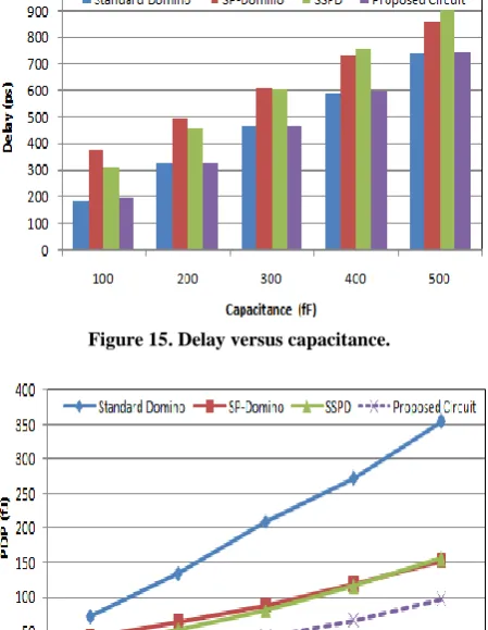
Comparison of power consumption of proposed circuit and existing circuits with clock frequency 200MHz where load capacitance is varied as shown in Fig.14. As a result, at higher load capacitance, our proposed circuit saves higher power consumption as compared to existing circuits. For capacitance 500fF, our proposed circuit reduces power consumption by 72.69%, 26.35% and 24.03% as compared to standard footless domino, SP-Domino and SSPD techniques. Our proposed circuit has better delay as compared to SP-Domino and SSPD techniques except standard footless domino circuit as shown in Fig.15. Our proposed circuit has better power delay product and at higher load capacitance its saving is large as compared to existing circuits as shown in Fig.16. Proposed circuit has better standby product as compared to SP-Domino technique and have higher value as compared to other exiting techniques as shown in Fig.17.
[image:6.595.320.545.74.228.2]Figure 14. Power consumption versus capacitance.
[image:6.595.318.543.84.374.2]Figure 15. Delay versus capacitance.
Figure 16. PDP versus capacitance.
Figure 17. Standby power versus capacitance.
[image:6.595.56.279.118.255.2] [image:6.595.57.281.442.628.2]Figure 18. Power consumption versus frequency.
Table 2. Comparison of power consumption (µW) of proposed circuit with the existing circuits.
Temperature (°C)
Standard Domino
SP-Domino
SSPD Proposed Circuit
30 389.56 112.95 95.19 51.09
50 382.81 112.75 93.89 51.31
70 359.59 112.84 93.33 51.58
90 339.88 112.75 94.04 51.54
[image:7.595.46.289.286.375.2]110 322.35 112.76 93.88 51.81
Table 3. Comparison of delay (ps) of proposed circuit with the existing circuits.
Temperature (°C)
Standard Domino
SP-Domino
[image:7.595.46.287.421.511.2]SSPD Proposed Circuit 30 185.11 376.58 312.52 197.39 50 196.42 385.81 331.49 208.26 70 208.13 398.51 352.47 219.80 90 220.35 415.11 374.42 232.19 110 233.77 432.91 398.93 245.37
Table 4. Comparison of delay (ps) of proposed circuit with the existing circuits.
Temperature (°C)
Standard Domino
SP-Domino
SSPD Proposed Circuit
30 72.11 42.53 29.74 10.08
50 75.19 43.50 31.12 10.68
70 74.84 44.96 32.89 11.33
90 74.99 46.80 35.21 11.96
110 75.35 48.81 37.45 12.71
Table 2 illustrates the relationship between the power consumption and temperature for proposed circuit and existing circuits, clock frequency and load capacitance were set 200MHz and 100fF. It shows proposed circuit has independent on temperature variation. At 110°C, proposed circuit reduces power consumption by 83.92%, 54.05% and 44.81% as compared to standard footless circuit, SP-Domino
circuit and SSPD circuit. Similarly, in Table 3 delay versus temperature is illustrated. Our proposed circuit suffer little delay penalty as compared to standard footless circuit and improves as compared to the other existing techniques. Table 4 shows PDP versus temperature, our proposed circuit has minimum PDP as compared to existing techniques.
Fig.19 illustrated the power consumption for proposed circuit and existing circuits for different power supply voltages. The clock frequency is set 200MHz and load capacitance is set 100fF. Our proposed circuit shows better power saving at higher power supply.
Figure 19. Power consumption versus power supply.
5.
CONCLUSION
Buffer circuit is essential to drive the output of the present stage into the next stage. Standard domino has redundant switching at dynamic and output node, this increases the dynamic power consumption of the circuit. In this paper a new circuit is proposed to work the domino as buffer. Pull up network of proposed circuit has combination of PMOS and NMOS transistor, and utilizes delayed clock. Dynamic node is conditional charged to high voltage only when both the transistors of pull up network turns ON and the pull down network turns OFF simultaneously at the start of each clock high for short duration of time. This technique passes the propagation of precharge pulse to the dynamic node and avoids to the output node, reduces the dynamic power consumption.
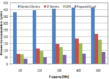
Proposed circuit and the existing circuits are simulated are simulated in 0.18µm using HSPICE. Performance of the proposed structure is compared with existing circuits for different clock frequency, loading condition and temperature. Our proposed circuit saves higher power consumption as compared to existing circuits. For capacitance 500fF, our proposed circuit reduces power consumption by 72.69%, 26.35% and 24.03% as compared to standard footless domino, SP-Domino and SSPD techniques. For operating frequency 500MHz, our proposed circuit reduces power consumption by 78.45%, 59.86% and 50.26% as compared to standard footless circuit, SP-Domino circuit and SSPD circuit.
ACKNOWLEDGMENT
The authors duly acknowledge with gratitude the support from ministry of communications and information technology, DIT Govt. of India, New Delhi, through special Manpower Development Program in VLSI and related Software’s Phase-II (SMDP-Phase-II) project in E&CE department, MNNIT
[image:7.595.45.287.556.650.2]6.
REFERENCES
[1] Wei. H, Josji. R. H and Henkels, 1999, “a 500-Mhz, 32-word, a 64 bit, eight-port self-resetting CMOS register file”, IEEE Tranactions on Solid-State Circuits, pp.56-67.
[2] Nowka. K. J and Galambos. T, 1998, “Circuit design techniques for a gigahertz integer microprocessor”, IEEE International Conference on Computer Design, pp.11-16. [3] Agrawal. A. K, Wairya. S, Nagaria. R.K,Tiwari. S,
2009, “Mixed gate diffusion input full adder topology for high speed low power digital circuits”, World Applied Sciences Journal (WASJ:Special Issue of Computer & IT), IDOSI Publication,vol.7,pp.138-144.
[4] Krambeck. R. H, Lee. C. M, and Law. H, 1982, “High-speed compact circuits with CMOS”, IEEE Journal of Solid-State Circuits, vol.SC-17, no.3, pp.614-619. [5] Thorp. T, Dean. L and Trivedi. P, 2003, “Analysis of
blocking dynamic circuits”, IEEE Transactions on VLSI Systems, pp.744-749.
[6] Charbel. J. A and Magdy. A. B, 2008, “Single-phase SP –domino:A limited-switching dynamic circuit technique for low-power wide fan-in logic gates “, IEEE Transactions on Circuits and Systems, vol.55,no.2, pp.141-145.
[7] Singh. R, Moon. G, Kim. M, Park. J, W, Shin. W. Y and Kim. S, 2012, “Static-switching pulse domino: A
switching-aware design technique for wide fan-in dynamic multiplexers”, Integratiom, The VLSI Journal, vol.45, pp.253-262.
[8] Tang. T and Bermak .A, 2012, “Low power TSPC-based domino logic circuit design with 2/3 clock load”, Transactions on Energy Procedia, vol.14, pp.1168-1174. [9] Ren.Y. J., Karlsson. J and Svensson, 1987, “A true
single-phase clock dynamic CMOS circuit technique”, IEEE Transactions on Solid-State Circuits, vol.22, no.5, pp.899-901.
[10] Jayakumaran. S, Hung. C. N, Kevin. J. N, Robert. K and Brown. B, 2005, “Controlled-load limited switch dynamic logic circuit”, IEEE Conference on Computer Society, pp.1-6.
[11] Fang. T, Amine. B and Zhouye. G, 2012, “Low power dynamic logic circuit design using a pseudo dynamic buffer”, Integration, the VLSI journal, vol.45, pp.395-404.
[12] Berkeley Predictive Technology Model (BPTM), http:// www.device.eecs.berkeley.edu/wptm/ download.htm. [13] Yee. G, Sechen. C, 2000, “Clock-delayed domino for