Abstract: In digital signal processing multiplication is frequently required. Parallel multipliers provide a high-speed method for multiplication, but require large area for VLSI implementations. A rounded product is desired to avoid growth in word size, in most signal processing applications. Thus an important design goal is to reduce the area requirement of the rounded output multiplier. This paper presents Field Programmable Gate Array (FPGA) which uses Very High Speed Integrated Circuit Hardware Description Language (VHDL) for the implementation of standard and truncated multiplier. Truncated multiplier is a good candidate for digital signal processing (DSP) applications such as finite impulse response (FIR) and discrete cosine transform (DCT) etc. Instead of standard parallel multipliers the significant reduction in FPGA resources, delay, and power is achieved by using truncated multipliers when the full precision of the standard multiplier is not required. The total project execution is done at Xilinx14.7 Spartan-3AN FPGA device.
Index Terms- Field Programmable Gate Array (FPGA), Digital Signal Processing (DSP), Truncated Multiplier, VHDL.
I.INTRODUCTION
MULTIPLICATION is one of the most area consuming arithmetic operations in high -performance circuits. As a consequence a research work deal with low power design of high speed multipliers. The generation of the partial products and their sum are the two basic operations in multiplication and these are performed by using two kinds of multiplication algorithms i.e., serial and parallel. Sequential circuits with feedbacks is used by serial multiplication
algorithm: The production and computation of inner products is sequential. Combinational circuits is often used by parallel multiplication algorithm and do not contain feedback structures. The output of multiplication of two bits is twice that of the original bit. For required precision to reduce area cost the truncation of partial product bits are needed. The computation of only n most significant bits (MSBs) of the 2n-bit product for n×n multiplication is made by Fixed-width multipliers, a subset of truncated multipliers which uses extra correction/compensation circuits to reduce truncation errors. In previous related papers, the adding of error compensation circuits is used to reduce truncation error. So that the output will be précised and during the design of fast parallel truncated multipliers we can jointly considers the tree reduction, truncation, and rounding of the PPbits in this approach so that the precision requirement is satisfied by final truncated product. In our approach truncation error is not more than 1ulp (unit of least position), so there is no need of error compensation circuits, and the final output will be précised.
In most signal processing applications, to avoid growth in word size the rounded product is required. Thus an important aim is to design a multiplier which required less area and that is possible with the truncated multiplier. DSP systems are ubiquitous in the wireless multimedia word. DSP algorithms test the limits of battery life in portable device such as cell phones, hearing aids, MP3 players, digital
High Speed and Area Efficient Truncating Multiplier for D.S.P
Applications
M. BHARATHI M.TECH – SCHOLAR – E.C.E
Dept. of E.C.E
GUNTUR ENGENERING COLLEGE GUNTUR DT.
P. MANAHOR RAO ASSISTANT PROFESSOR
Dept. of E.C.E
video recorders and so on and these are computationally intensive. In many signal processing algorithms the multiplication is the main operation and hence efficient parallel multipliers are desirable. The computation of the 2n bits output as a weighted sum of partial products is by a full-width digital n x n bits multiplier. A multiplier with the output represented on n bits output is useful, as example, in DSP data paths which saves the output in the same n bits registers of the input. The n-bits outputs is obtained by a truncated multiplier which is an n x n multiplier. Since in a truncated multiplier the n less significant bits of the full-width product are discarded, some of the partial products are removed and replaced by a suitable compensation function, to trade-off accuracy with hardware cost. As more columns are eliminated, the area and power consumption of the arithmetic unit are significantly reduced, and in many cases the delay also decreases.
The introductionof additional error into the computation is by truncating the multiplier matrix. Recent advancements in VLSI technology and in particular, the increasing complexity and capacity of state-of-the-art programmable logic devices have been making hardwareemulations possible. The SRAM-based field programmable gate arrays (FPGAs) is used by underlying key of the emulation system which are very flexible and dynamically reconfigurable. In many cases implementation of DSP algorithm demands using Application Specific Integrated Circuits (ASICs).The development cost for Application Specific Integrated Circuits (ASICs) are high, algorithms should be verified and optimized before implementation. The extensive use of multiplication is required by Digital Signal Processing(DSP) image processing and multimedia.
II.EXISTED SYSTEM
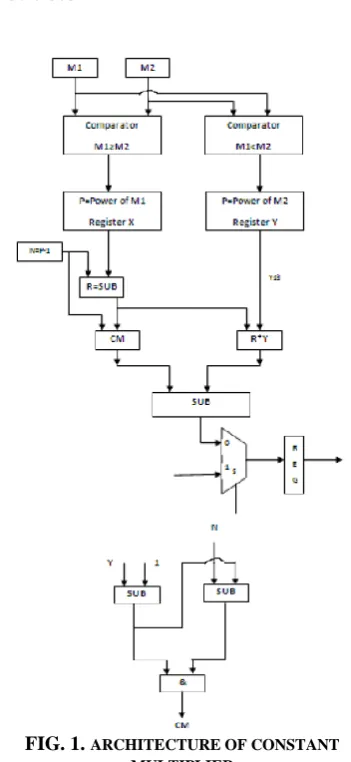
In latest VLSI era more and more gates are deployed in asingle chip. Figure show that Modular and Scalablearchitecture of recursive constant multiplier it should have a optimal use of the processing power. The ConstantMultiplier (CM) block can be reused upto low order wordsizeto achieve lesser power consumption. The overall performance of the architecture is significantly better. The hardware architecture isstraightforward and simple followed by Multiplexer, Comparator, Subtractor and Half-Subtractor.
FIG. 1. ARCHITECTURE OF CONSTANT MULTIPLIER
chip. Figure show that Modular and Scalablearchitecture of recursive constant multiplier it should have a optimal use of the processing power. The ConstantMultiplier (CM) block can be reused upto low order wordsizeto achieve lesser power consumption. The overall performance of the architecture is significantly better. The hardware architecture isstraightforward and simple followed by Multiplexer,Comparator, and Half-Adder. The existing architecture deficiency in terms of timing as themultiplier size has been increased and this is improved in theproposed architecture.
The CM result and multiplier output is again adder to get finalmultiplication. The proposed architecture built using basic data-pathelements. To handle the corner cases the multiplexer blockis utilized. Any of the primary input is low the multiplieroutput is generated directly zero. The select line is logichigh based on constant multiplier algorithm then themultiplexer output is generated. The resultant multiplexeroutput is stored in the memory element.
III.PROPOSED SYSTEM
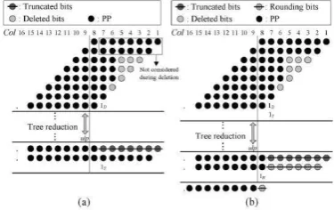
The objective of a good multiplier is to provide a physically compact, good speed and low power consuming chip. To save significant power consumption of a VLSI design. In a truncated multiplier, several of the least significant columns of bits in the partial product matrix are not formed. This reduces the area, power consumption, and also the delay of the multiplier in many cases, because the carry propagate adder producing the product can be shorter. 3.1 Deletion, Reduction, and Truncation In the first step deletion operation is performed, that removes all the avoidable
partial product bits which are shown by the light gray dots (fig 2). Delete as many partial product bits as possible in this deletion operation. In Fig. 2, by skipping the first two of partial product bits the deletion of partial product bits starts from column 3. After the deletion of partial product bits, perform column-by- column reduction of scheme 2.
After the reduction, perform the truncation, which will further removes the first row of (n-1) bits from column 1 to column (n-1). The most significant columns with the variable correction method. It also presents a comparative study of (FPGA) implementation of standard and truncated multipliers using very high speed. Significant reduction in FPGA resources, delay, and power can be achieved using truncated multipliers instead of standard parallel multipliers when the full precision of the standard multiplier is not required.
Fig. 2 8x8 truncated multiplication.(a) deletion, reduction and truncation. (b) Deletion, reduction, truncation, and final addition.
response of the filter .This is what all digital filters do. However, the FIR filter has the following differentiating characteristics. The FIR filter is non recursive: It uses a finite duration of non-zero input values and produces a finite duration of the output values which are non-zero. FIR filters use addition to calculate their outputs just like averaging does. The delays, multipliers and adders are the primitive elements used in the design of a FIR filter. The FIR filter consists of a series of delays, multiplications and additions as to produce the time domain output response. The multiplication coefficients used is the impulse response of the FIR filter. The phase of a FIR filter is linear. The frequency response of the FIR filter is the DFT (Discrete Fourier Transform). The method of multiplication is improved based upon the proposed method which reduces delay and complexity of the process.
The new method for parallel multiplication which computes the products of two n bit numbers by summing only the most significant columns with the variable correction method. It also presents a comparative study of (FPGA) implementation of standard and truncated multipliers using very high speed. Significant reduction in FPGA resources, delay, and power can be achieved using truncated multipliers instead of standard parallel multipliers when the full precision of the standard multiplier is not required. We can multiply 8x8 bits, and the bits are reduced in step by step manner in proposed architecture. Deletion is the first operation performed in Stage 1 to remove the PP bits, as long as the magnitude of the total deletion error is no more than 2−P−1. To reduce the final bit width without increasing the error the number of stages are required. In normal truncated multiplier design, the architecture
produces the output with some truncation error.
IV.RESULTS
RTL SCHEMATIC
TECHNOLOGY SCHEMATIC
OUTPUT WAVE FORM
V.CONCLUSION
VI.REFERENCES
[1] R. L. Rivest, A. Shamir, and L. Adleman, “A method for obtaining digitalsignatures and public-key cryptosystems,” Commun. ACM, vol. 21, no. 2,pp. 120–126, Feb. 1978.
[2] V. S. Miller, “Use of elliptic curves in cryptography,” in Advances inCryptology. Berlin, Germany: Springer-Verlag, 1986, pp. 417–426. [3] N. Koblitz, “Elliptic curve cryptosystems,”
Math. Comput., vol. 48,no. 177, pp. 203–209,
1987.
[4] P. L. Montgomery, “Modular multiplication without trial division,” Math.Comput., vol. 44, no. 170, pp. 519–521, Apr. 1985.
[5] Y. S. Kim, W. S. Kang, and J. R. Choi, “Asynchronous implementationof 1024-bit modular processor for RSA cryptosystem,” in Proc.
2ndIEEE Asia-Pacific Conf. ASIC, Aug. 2000, pp.
187–190.
[6] V. Bunimov, M. Schimmler, and B. Tolg, “A complexity-effectiveversion of Montgomery’s algorihm,” in Proc. Workshop Complex.Effective
Designs, May 2002.
[7] H. Zhengbing, R. M. Al Shboul, and V. P. Shirochin, “An efficientarchitecture of 1024-bits cryptoprocessor for RSA cryptosystem basedon modified Montgomery’s algorithm,” in Proc. 4th IEEE Int. WorkshopIntell. Data Acquisition Adv.
Comput. Syst., Sep. 2007, pp. 643–646.
[8] Y.-Y. Zhang, Z. Li, L. Yang, and S.-W. Zhang, “An efficient CSAarchitecture for Montgomery modular multiplication,”
MicroprocessorsMicrosyst., vol. 31, no. 7, pp. 456–
459, Nov. 2007.
[9] C. McIvor, M. McLoone, and J. V. McCanny, “Modified Montgomerymodular multiplication and RSA exponentiation techniques,” IEE
Proc.Comput. Digit. Techn., vol. 151, no. 6, pp.
402–408, Nov. 2004.
[10] S.-R. Kuang, J.-P. Wang, K.-C. Chang, and H.-W. Hsu, “Energy-efficienthigh-throughput Montgomery modular multipliers for RSA cryptosystems,”IEEE Trans. Very Large Scale
Integr. (VLSI) Syst., vol. 21, no. 11,pp. 1999–2009,
Nov. 2013.
[11] J. C. Neto, A. F. Tenca, and W. V. Ruggiero, “A parallel k-partitionmethod to perform Montgomery multiplication,” in Proc. IEEE Int.
Conf.Appl.-Specific Syst., Archit., Processors, Sep.
2011, pp. 251–254.
[12] J. Han, S. Wang, W. Huang, Z. Yu, and X. Zeng, “Parallelization ofradix-2 Montgomery multiplication on multicore platform,” IEEE
Trans.Very Large Scale Integr. (VLSI) Syst., vol.
21, no. 12, pp. 2325–2330, Dec. 2013.
[13] P. Amberg, N. Pinckney, and D. M. Harris, “Parallel high-radixMontgomery multipliers,” in
Proc. 42nd Asilomar Conf. Signals, Syst.,Comput.,
Oct. 2008, pp. 772–776.
[14] G. Sassaw, C. J. Jimenez, and M. Valencia, “High radix implementationof Montgomery multipliers with CSA,” in Proc. Int. Conf.
Microelectron.,Dec. 2010, pp. 315–318.
[15] A. Miyamoto, N. Homma, T. Aoki, and A. Satoh, “Systematicdesign of RSA processors based on high-radix Montgomery multipliers,”IEEE
Trans. Very Large Scale Integr. (VLSI) Syst., vol.