1817
Effects of Using p
+
-CdTe as a BSR Layer for CdTe
Based Solar Cells
1Harshleen Kaur, 2Rajesh Mehra
Electronics and communication1,2, M.E Scholar1, Associate Professor2 NITTTR, Chandigarh-160019, India1,2
Email: [email protected], [email protected]
Abstract- This paper deals with the modified structure of CdTe based solar cells. The Zinc Telluride (ZnTe) back surface reflector (BSR) layer is replaced by p+- CdTe layer in order to improve the efficiency of the cell. It is introduced between metal back contact and CdTe absorber layer, to reduce the possible recombination at the back contact and the effect of the roll over in the ultrathin CdTe solar cells. This layer can contribute to increasing of 𝑉OC and could also contribute in the carrier enhancement by reflecting the carriers towards the main
junction. Modified solar cell with high efficiency of 17.86% was obtained.
Index Terms- CdTe Solar cell; BSR Layer; Numerical Simulation; Efficiency
1. INTRODUCTION
Fossil fuels are limited and non-renewable source of energy. Moreover, use of non-renewable sources of energy is harmful to the environment. In order to meet the increasing energy demands, use of renewable energy resources should be increased. It also helps in sustainable development. Out of five regularly used renewable energy sources (Biomass, water, sun, wind and geothermal), this work is based on solar energy. Photovoltaic or solar cell conversion is the simplest and clean transformation of solar energy to electricity requiring low maintenance yet exceptionally good outputs. Because of its advantages, and easy handling qualities coupled with uncountable benefits, the interest of researchers in PV technologies is increasing day by day. Since solar energy is available during the day only and sometimes affected by climatic conditions also, it must be stored carefully and reliably for usage at odd times. For this, extremely efficient solar cells as well as modules need to be developed [1].
Several types of solar cells based on crystalline Silicon [2], thin-film technology [3,4], organic materials [5,6] and many more are gradually developed in past decades. Out of the oldest technologies, „Crystalline Silicon (c-Si) PV‟ are ruling approximately 80 to 90% of world‟s photovoltaic market with advantages like easy and abundant availability, high stability, durable high-quality cell, outstanding conversion efficiency, non-toxic nature, the possibility of reducing cost, and many more. Thin film technology has emerged during the last decades and has entered into direct competition with traditional multicrystalline silicon technology, which still dominates the market of photovoltaic [7].
One of the most promising thin film technologies is CdTe solar cells which provides better efficiency/cost ratio in contrast to other technologies. Bandgap of CdTe is approximately ~1.5eV, which is very close to
the ideal value for photovoltaic conversion efficiency. Its high optical absorption coefficient and high chemical stability makes it a very attractive material for thin film solar cells. 28%–30% is the expected theoretical efficiency of CdTe thin-film solar cells, but the achieved efficiencies are still much below than theoretical efficiency providing an attractive area for research. Therefore, there is a large scope for the improvement in CdTe solar cell performance [8].
Performance of CdTe based solar can be improved significantly by using appropriate BSR layer. It is introduced between metal back contact and CdTe absorber layer, to reduce the possible recombination at the back contact and the effect of the roll over in the ultrathin CdTe solar cells. This layer can contribute to increasing of 𝑉OC and could also contribute in the
carrier enhancement by reflecting the carriers towards the main junction. In this work the ZnTe layer used in the structure proposed in [9] is replaced by p+- CdTe layer [10] in order to enhance the CdTe solar cell performance.
2. MATERIALS AND MODELING
The numerical modeling of the proposed structure is done with the help of Solar Cell Capacitance Simulator in 1 Dimension (SCAPS-1D) developed by burgelman et al [11]. I-V characteristics of proposed structure are investigated and then compared with the conventional structure. SCAPS is a one dimensional solar cell simulation program developed at the department of Electronics and Information Systems (ELIS) of the University of Gent, Belgium. The main functionality of SCAPS is to solve the one dimensional semiconductor equations [12]. In the bulk of the layers these eauqtions are given by Eq. (1) to Eq. (5) as shown below:
1818 Conventional CdTe solar cell structure is modified by
replacing the ZnTe BSR layer with p+-CdTe BSR layer. In figure 1(a) the conventional solar cell structure with ZnTe BSR layer is shown whereas in figure 1(b) the modified solar cell structure with p+ -CdTe BSR layer is shown.
(a) (b)
Figure 1. (a) Conventional solar cell with ZnTe BSR layer (b) Proposed solar cell with p+-CdTe BSR layer
[image:2.595.315.511.97.230.2]The selection of material parameters used in this work is done on the basis of some reasonable estimation and by referring the simulation procedures mentioned in [9] and [10]. Parameters used in this work are listed in table 1 and table 2.
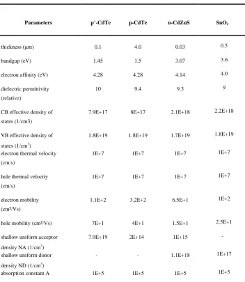
Table 1. Selection of material parameters
Parameters p+-CdTe p-CdTe n-CdZnS SnO
2
thickness (μm) 0.1 4.0 0.03 0.5
bandgap (eV) 1.45 1.5 3.07 3.6
electron affinity (eV) 4.28 4.28 4.14 4.0
dielectric permittivity 10 9.4 9.3 9
(relative)
CB effective density of 7.9E+17 8E+17 2.1E+18 2.2E+18
states (1/cm3)
VB effective density of 1.8E+19 1.8E+19 1.7E+19 1.8E+19
states (1/cm3)
electron thermal velocity 1E+7 1E+7 1E+7 1E+7
(cm/s)
hole thermal velocity 1E+7 1E+7 1E+7 1E+7
(cm/s)
electron mobility 1.1E+2 3.2E+2 6.5E+1 1E+2
(cm²/Vs)
hole mobility (cm²/Vs) 7E+1 4E+1 1.5E+1 2.5E+1
shallow uniform acceptor 7.9E+19 2E+14 1E+15 -
density NA (1/cm3)
shallow uniform donor - - 1.1E+18 1E+17
density ND (1/cm3)
absorption constant A 1E+5 1E+5 1E+5 1E+5
Jn= qμnnε + qDn
dn
dx= qμn nε + kT
q dn dx = μnn
dEFn
dx (1)
Jp= qμppε + qDp
dp
dx= qμp pε + kT
q dp dx = μpp
dEFp
dx (2)
−∂Jn
∂x− Un+ G = ∂n
∂t (3)
−∂Jp
∂x− Up+ G = ∂p
∂t (4)
∂ ∂x ε0ε
∂Ψ
[image:2.595.71.288.105.238.2] [image:2.595.124.477.360.765.2]1819
(1/cm eV(½))
Defect type - Donor Acceptor Donor
Capture cross section - 1E-12 1E-17 1E-12
electrons (cm²)
capture cross section - 1E-15 1E-12 1E-15
holes (cm²)
energetic distribution - Gaussian Gaussian Gaussian
reference for defect - Above Ev Above Ev Above Ev
energy level Et -
energy level with respect - 0.600 0.600 0.600
to Reference (eV)
[image:3.595.121.475.109.303.2]Nt total (1/cm3) uniform - 2E+14 1E+18 1E+15
Table 2. Front and back contact parameters
Parameters Back contact Front contact
surface recombination velocity of electrons (cm/s) 1.000E+7 1.000E+7
surface recombination velocity of holes (cm/s) 1.000E+7 1.000E+7
Metal work function (eV) - -
Majority Carrier barrier height relative to Ef (eV) - -
Majority Carrier barrier height relative to Ev (eV) - -
3. RESULTS AND DISSCUSION
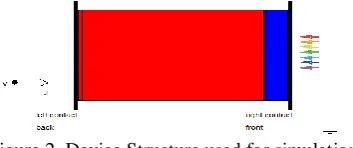
With the help of SCAPS-1D, numerical simulation of the structure shown in figure 1(b) was performed to observe the behavior of the proposed solar cell after replacing ZnTe BSR layer with p+-CdTe BSR layer. After that obtained results were compared with the conventional strucutre. The simulated strucutre is shown in figure 2.
[image:3.595.51.549.339.456.2]Figure 2. Device Structure used for simulation
Figure 3 shows the I-V characteristics of the proposed structure. Efficiency, VOC and JSC were increased from
[image:3.595.95.272.593.667.2]17.71% to 17.86%, 0.922V to 1.1124V and 25.468 mA/cm2 to 25.590 mA/cm2, respectively. Whereas, fill factor was reduced from 75.4% to 62.75% as shown in table 3.
1820 Table 3. Comparison of both cells
Cell solar cell
(conventional)
solar cell (proposed)
Voc (V) 0.922 1.1124
Jsc
(mA/cm2) 25.468 25.590
FF (%) 75.4 62.75
Efficiency
(%) 17.71 17.86
It can be observed from the comparison results shown in table 3 that efficiency, VOC and JSC were enhanced
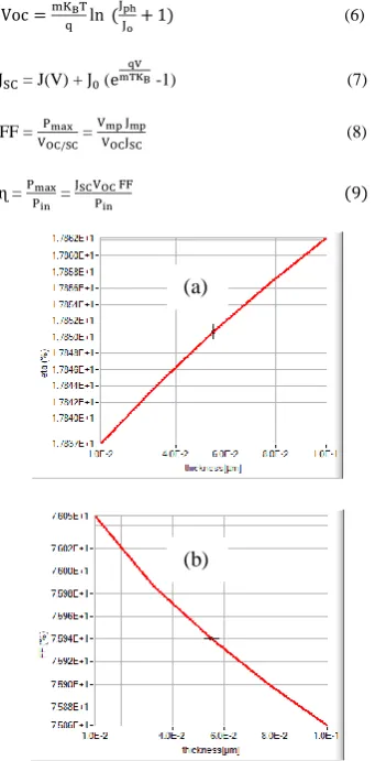
significantly. The p+-CdTe BSR layer has great influence on I-V characteristics of the cell and leads to better performance. The variation in CdTe solar cell parameters in accordance with the p+-CdTe BSR layer thickness is shown in figure 4. As observed in table 4, with increase in the thickness of p+-CdTe BSR layer efficiency of the cell also increases. Simulations were carried out by taking BSR layer thickness in the range of 0.01 to 0.1 µm. Variations in cell parameters can be justified by the equations given below.
[image:4.595.88.277.122.272.2]
Figure 4. Variation of cell parameters in accordance with P+-CdTe BSR layer
Table 4. Summary of the simulated results at varying thickness of P+CdTe layer.
Thickness (µm)
VOC (V) JSC (mA/cm2) FF
(%)
ɳ (%)
0.010 1.1114 25.518606 62.89 17.84
0.040 1.1117 25.546200 62.84 17.85
0.060 1.1120 25.562354 62.80 17.85
0.080 1.1122 25.577109 62.77 17.86
0.100 1.1124 25.590653 62.75 17.86
Table 4 shows that VOC increases from 1.1114V to
1.1124V as the BSR layer thickness increases from 0.01 µm to 0.1 µm. similarly JSC and efficiency also
increases from 25.518606 to 25.590653 mA/cm2 and 17.84 to 17.86% as the BSR layer thickness increases from 0.01 µm to 0.1 µm. Whereas FF decreases from 62.89 to 62.75% with increasing BSR layer thickness.
4. CONCLUSION
CdTe solar cell structure with 0.1 µm thick p+-CdTe layer was designed. Numerical simulations were carried out by the variation of BSR layer thickness. It is shown that solar cell with p+-CdTe as a BSR layer has significant improvement in efficiency. Effects of modifying the solar cell structure were investigated
Voc =mKBT q ln (
Jph
Jo + 1) (6)
JSC = J(V) + J0(e
qV
mTKB -1) (7)
FF = VPmax OC/SC =
Vmp Jmp
VOCJSC (8)
ɳ = Pmax
Pin =
JSCVOC FF
Pin (9)
(a)
(b)
(c)
[image:4.595.97.268.420.766.2] [image:4.595.303.529.435.577.2]1821 effectively with the help of numerical simulations. The
research of the BSR layer optimization provides constructive guidelines for the future design and fabrication of CdTe solar cells.
5. ACKNOWLEDGMENT
We would like to thank Director and Head of Electronics and Communication Engineering Department, National Institute of Technical Teacher‟s Training and Research, Chandigarh, India for their support and inspiration. Also, we appreciate the efforts of Prof. M. Burgelman and his colleagues for developing SCAPS and we are thankful to them for permitting us to use it for the research work.
REFERENCES
[1] Bhubaneswari Parida, S. Iniyan, Ranko Goic , “A review of solar photovoltaic technologies”, Renewable and Sustainable Energy Reviews, Vol. 15, pp. 1625–1636, 2011.
[2] Yan, B. Yue, G. Xu, X. Yang, J. and Guha, S, “High efficiency amorphous and nanocrystalline silicon solar cells” Physica Status Solidi A, Vol. 207, No. 3, pp. 671-677, 2010.
[3] M. A. Green, “Thin-film solar cells: review of materials technologies and commercial status” Journal of Materials Science in Electronics, Vol. 18, No. 10, pp. S15-S19, 2007.
[4] V. Fthenakis, “Sustainability of photovoltaics: the case for thin film solar cells” Renewable and Sustainable Energy Reviews, Vol. 13, No. 9, pp. 2746-2750, 2009.
[5] Kietzke, T. 2007.Recent advances in organic solar cells. Advances in OptoElectronics, 2007, Article ID 40285.
[6] L. Ren, and S. Wang, “Progress of organic photovoltaic materials” Recent Patents on Materials Science, Vol. 3, No.1, pp. 26-39, 2010. [7] Teyou Ngoupo, A. Ouédraogo, S. Zougmoré, F.
and Ndjaka J.M.B. 2015.New Architecture towards Ultrathin CdTe Solar Cells for High Conversion Efficiency. International Journal of Photoenergy, 2015, Article ID 961812: 9 pages
[8] Xiaobo Xu, Xiaoyan Wang, Wenping Gu, Si Quan and Zan Zhang. 2017.Study on influences of CdZnS buffer layer on CdTe solar cells. Superlattices and Microstructure, DOI: 10.1016/j.spmi.2017.05.033
[9] Xiaobo Xu, Xiaoyan Wang, Wenping Gu, Si Quan, Zan Zhang, “Study on influences of CdZnS buffer layer on CdTe solar cells”, Superlattices and Microstructures (2017), doi: 10.1016/j.spmi.2017.05.033
[10] A. Teyou Ngoupo, S. Ouédraogo, F. Zougmoré and J. M. B. Ndjaka, “New Architecture towards Ultrathin CdTe Solar Cells for High Conversion Efficiency”, International Journal of Photoenergy,
Vol. 2015, Article ID 961812, 9 pages, 2015, http://dx.doi.org/10.1155/2015/961812.
[11] Burgelman, M. Nollet, P. and Degrave. S. “Modelling polycrystalline semiconductor solar cells”, Thin Solid Films, Vol. 361, pp. 527-532, 2000.
[12] Burgelman Marc, Decock Koen, Niemegeers Alex, Verschraegen Johan, Degrave Stefaan, SCAPS Manual, Version: 29, december 2016.
Back Contact
P+-CdTe
p-CdTe
N-CdZnS
TCO (SnO2)