High Speed Area Efficient Diminished-1
Modulo
2
n
1
Multiplier
Ahana Mishra, Swapnil Jain, Jyoti Dangi
M. Tech. Scholar, Dept. of Electronics & Communication , NIIST, Bhopal, Madhya Pradesh, India
Assistant Professor, Dept. of Electronics & Communication , NIIST, Bhopal, Madhya Pradesh, India
Assistant Professor, Dept. of Electronics & Communication , NIIST, Bhopal, Madhya Pradesh, India
ABSTRACT: Modular adder is one of the key components for the application of residue number system (RNS). Moduli set with the form of 2n +1 can offer excellent balance among the RNS channels for multi-channels RNS processing. As one of the processor's ALU performance issues, the carry propagation during the addition operation limits the speed of arithmetic operation. In this paper review on 2n +1 addition in the residue number system. The architecture design of CCS modular adder is simple and regular for various bit-width inputs. The review modulo adder in the aforementioned paper consists of a dual-sum carry look-ahead (DS-CLA) adder, a circular carry generator, and a multiplexer, which can reduce both number of slice and maximum combination path delay (MCPD).
KEYWORDS: Modulo Adder, Residue Number System (RNS), and VLSI design
I. INTRODUCTION
A Residue number system is a non-weight numeric system [1] which has gained importance during the last decade, because some of the mathematical operations can be divided into categories of sub-operations based on RNS [2]. Addition, subtraction and multiplication are performed in parallel on the residues in distinct design units (often called channels), avoiding carry propagation among residues [3]. Therefore, arithmetic operations such as, addition, subtraction and multiplication can be carried out more efficiently in RNS than in conventional two's complement systems. That makes RNS a good candidate for implementing variety of applications [4] such as: digital Signal Processing (DSP) for filtering, convolutions, FFT computation, fault-tolerant computer systems, communication and cryptography.
II. DIMINISHED-1NUMBERREPRESENTATION
The modulo arithmetic operations require (n+1) bit operands. To avoid (n+1)-bit circuits, the diminished-1 number system [15] has been adopted. Let be the diminished-1 representation of the normal binary number
, namely
(i)
In (i), when, is an n -bit number, therefore (n+1) -bit circuits can be avoided in this case. However,
(ii)
is an (n+1) -bit number. This leads to special treatment for d [0]. The diminished-1 arithmetic operations [15] are defined as
(iii)
(iv)
(v)
(vi)
(vii)
(viii)
Where represents the one’s complement of d [A]. In (vii) and (viii) iCLS (d[a], k) is the k -bit left-circular shift of in which the bits circulated into the LSB are complemented.
III. MODULO ADDER
Figure 1: Proposed binary to residue converter – (a) modulo (2 n – 1) channel
(b) Modulo (2 n + 1) channel
The most difficult residue to obtain is the one with respect to (2n + 1) modulo. Typically, this one requires modulo (2n + 1) sub tractor followed by modulo (2n + 1) adder. This structure is rather complicated, since both components are complex and time consuming. However, by a proper extraction of the equations needed for the forward conversion process, the proposed structure of the component that computes the residue with respect to modulo (2n + 1) is considerably simplified. It is realized using two parallel binary adders followed by modulo (2n + 1) adder as illustrated in Figure 1 (b). Since one of the inputs of the first binary adder is constant, its structure can be simplified, the (n + 1) full adders can be replaced by (n – 2) half adders. However, this simplification does not reduce the delay (due to the second adder that adds B1 + B3), but the overall hardware complexity decreases.
Majority of the published structures of modulo (2n – 1) adder perform addition first, and then apply the necessary correction, in order to get the correct result that corresponds to this modulo. The standard structure of this adder depends on two binary adders and a multiplexer. However, the proposed modular adder employs the prefix adders’ concept in order to pre calculate the carry-out needed for the correction process. This design has been published in an international conference in Brno [1] and an extended version has been published in Electro Scope journal.
IV. MODULO (2N +1) ADDER – BASED ON PREFIX CARRY COMPUTATION
Contrary to the previously proposed modulo (2n + 1) adder, this one consists of (n + 1) -bit circuits. However, it utilizes the concept of prefix carry computation used in parallel prefix adders in order to speed-up the computation process. This modular adder has been published in an international conference in Brno [2] and an extended version has been published in Electro Scope journal.
The structure of the proposed adder is illustrated in Figure 2. The main concept of this adder is based on the prefix computation of the MSB of (X + Y – 1), and then applying the necessary correction. This correction is represented in applying the correct carry-in into the CRA. To prove the efficiency of this adder, it was compared with another already published one, which was published in [9] and denoted as (k). This Modular adder (k) was chosen due to its superiority over other modular adders stated in [9]. Both adders were implemented on Spartan-3 xc3s200 FPGA.
output
8-bit inverted EAC CSA
8-bit inverted EAC CSA
8 8 8 8
8-bit inverted EAC CSA 8
CT PP3 PP2 PP1 PP0
2-Stage Inverted n-bit Adder
a7 a6 a2 a1 a0 a7 a8 b
b 1 b BS
+ BS+
BS
+ BS+ BE0
PP0(7) PP0(3) PP0(2) PP0(0)
PP3(7) PP3(3) PP3(2) PP3(0)
a1 a0 a4 a3 a2 a1 a8
b 7 b BS
+ BS
- BS
-BS- BE
xno r
xno r
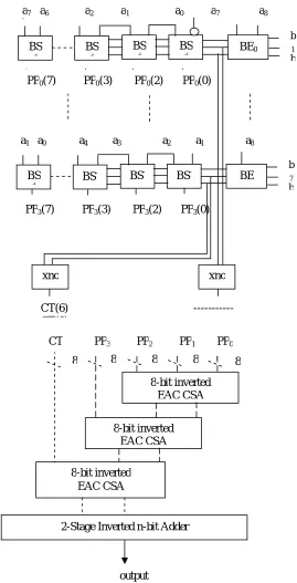
The proposed architecture in fig.1 take two input of n bit as d[A] and B and gives result as 2 1
A
B
nP
.Whered[A] is the diminished-1 representation of A.
V. RESULTANDSIMULATION
All the designing and experiment regarding algorithm that we have mentioned in this paper is being developed on Xilinx 14.1i updated version. Xilinx 9.2i has couple of the striking features such as low memory requirement, fast debugging, and low cost. The latest release of ISETM (Integrated Software Environment) design tool provides the low memory requirement approximate 27 percentage low. ISE 14.1i that provides advanced tools like smart compile technology with better usage of their computing hardware provides faster timing closure and higher quality of results for a better time to designing solution. ISE 14.1i Xilinx tools permits greater flexibility for designs which leverage embedded processors. The ISE 14.1i Design suite is accompanied by the release of chip scope ProTM 14.1i debug and verification software. By the aid of that software we debug the program easily. Also included is the newest release of the chip scope Pro Serial IO Tool kit, providing simplified debugging of high-speed serial IO designs for Virtex-4 FX and Virtex-5 LXT and SXT FPGAs. With the help of this tool we can develop in the area of communication as well as in the area of signal processing and VLSI low power designing. To simplify multi rate DSP and DHT designs with a large number of clocks typically found in wireless and video applications, ISE 14.1i software features breakthrough advancements in place and route and clock algorithm offering up to a 15 percent performance advantage. Xilinx 14.1i Provides the low memory requirement while providing expanded support for Microsoft windows Vista, Microsoft Windows XP x64, and Red Hat Enterprise WS 5.0 32-bit operating systems.
Maximum combinational path delay: 37.822ns Figure 4: Device summary of 8-bit residue number
Figure 5: Device summary of 12-bit residue number
Figure 6: Device summary of 16-bit residue number
Maximum combinational path delay: 43.916ns
V. CONCLUSION
The main aim of this paper was designing RNS based building blocks for applications in the field of DSP applications (binary-to-residue converter, residue-to-binary converter and residue adder.
The main RNS components have been introduced including a binary to residue converter, modular adders, modular sub tractors, modular multipliers, a residue comparator, components for overflow and sign detection and correction and a residue to binary converter. The antithesis to the prevalent issue regarding the number of moduli within a set has been also presented. The three-moduli set {2n+1 – 1, 2n, 2n – 1} have shown the best timing performances among all other sets.
REFERENCES
[1] P. V. Ananda Mohan, Residue Number Systems: Algorithms and Architectures, Kluwer, Academic Publishers, 2002.
[2] MOHAN, P.V.A., Residue Number System: Algorithms and Architectures. Massachusetts: Springer, 2002. 272 pages. ISBN-13: 978-1402070310.
[3] PIESTRAK, S.J. A High-Speed Realization of a Residue to Binary Number System Converter. In IEEE Trans. on Circuits and Systems-II: Analog and Digital Signal Processing, 1995, vol. 42, p. 661 – 663. ISSN 1057-7130.
[4] MOHAN, P.V.A. RNS-to-Binary Converter for a New Three-Moduli Set {2n+1 – 1, 2n , 2n – 1}. In IEEE Trans. on Circuits and Systems-II: Express Briefs, 2007, vol. 54, p. 775 – 779. ISSN 1549-7747.
[5] MOLAHOSSEINI, A.S., NAVI, K., RAFSANJANI, M.K. A New Residue to Binary Converter Based on Mixed-Radix Conversion. In 3rd International Conference on Information and Communication Technologies: From Theory to Applications, 2008, p. 1 – 6. ISBN 978-1-4244-1751-3.
[6] BI, S., GROSS, W.J. Efficient Residue Comparison Algorithm for General Moduli Sets. In 48th Midwest Symposium on Circuits and Systems, 2005, vol. 2, p. 1601 – 1604. ISBN 0-7803-9197-7.
[7] WANG, W., SWAMY, M.N.S., AHMAD, M.O., WANG, Y. A Study of the Residue-to-Binary Converters for the Three-Modulus Sets. In IEEE Trans. on Circuits and Systems-I: Fundamental Theory and Applications, 2003, vol. 50, p. 235 – 243. ISSN 1057-7122.
[8] MOLAHOSSEINI, A.S., TEYMOURI, F., NAVI, K. A New Four-Modulus RNS to Binary Converter. In Proc. of IEEE International Symposium on Circuits and Systems, 2010, p. 4161 – 4164. ISBN 978-1- 4244-5308-5.
[9] A. Curiger, H. Bonnenberg, and H. Kaeslin, “Regular VLSI architectures for multiplication modulo(2n1) ,” IEEE J. Solid-State Circuits,vol. 26, no. 7, pp. 990–994, Jul. 1991.
[10] L. Leibowitz,“A simplified binary arithmetic for the fermat number transform,” IEEE Trans. Acoust., Speech, Signal Process., vol. ASSP-24, pp. 356–359, May 1976.
[11] J.W.Chen, R.H.Yao and W.J.Wu,Efficient “modulo (2n 1) multipliers,” IEEE Trans. VLSI systems., vol. 19, no 12, pp. 2149–2157, Dec.
2011.