ANN Based DC-DC Converter for Renewable
Energy Based Servo Drives
Ramakrishnaprabu.G 1, Ramesh.T2
Associate Professor, Dept. of. EEE, VMKV Engineering College, Salem, Tamilnadu, India1 PG Student [PSE], Dept. of EEE, VMKV Engineering College, Salem, Tamilnadu, India2
ABSTRACT:Now days the electric power utility is raised due to the presence of more no of peoples, if it is continued
one day the power demand may increase, hence the new kind of source investigation is essential to build our live style effectively. Recently the Renewable energy source is identified as a alternative for conventional electric source. The renewable energy such as Wind and Photo-Voltaic (PV) arrays are widely using in automobiles, industries, residential and commercial buildings, all the systems energy storage devices are required for backup the power. Hence I would like to propose the renewable energy based servo drives.In the Proposed system the Full bridge with three port converters based systematic method is developed. The MOSFET hex bridge consists of two bidirectional ports and an isolated output port. The primary circuit of the converter functions as a boost converter and provides a power flow path between the ports on the primary side. The three port converter features single stage conversion between any two of the three ports and closed loop with feedback circuit. Its result is higher system efficiency, fewer components, faster response and compact packaging. The Boost converter can adapt to a wide source voltage range and servo drive runs at constant speed for various load conditions by using the ANN controller.
KEYWORDS: Photovoltaic, Full Bridge with three port network, Servo Drive, Artifical Neural Network (ANN)
I. INTRODUCTION
Fully isolated MPCs are typically derived by combining full-bridge, half-bridge, or series-resonant topologies via magnetic coupling, e.g., utilizing multi winding transformers. Isolation and bidirectional capabilities of all the ports and ZVS can be achieved in these topologies. These MPCs are good candidates for the applications where isolation and bidirectional conversion are required. However, the major problem is that too many active switches are used. This results in complicated driving and control circuitry, which may degrade the reliability and performance of the integrated converters. Non isolated MPCs can either be derived by using dc-link or integration method. These MPCs feature compact design and high power density. However, voltage levels of all ports are not flexible, and ZVS cannot be achieved easily. Partly isolated MPCs are based on hybrid topologies of isolated circuits and non-isolated circuits, which can provide the necessary isolation for the load with flexible voltage levels and maintain advantages of compact design and high power density. A boost-integrated MPC has been presented by combining a PS-FBC and a boost converter. The power flow control has been realized by using PWM plus phase-angle-shift control scheme. This principle is further applied to the three-phase FBC. These MPCs have some common features, i.e., the structures of the primary side circuit are similar. However, they have only rarely been examined and investigated in terms of their relationships, topological characteristics, or how to derive these topologies.
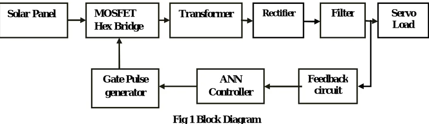
II. BLOCK DIAGRAM
Fig 1 Block Diagram Explanation
The fig 1 shows the block diagram of the proposed method. By using the method the servo load runs with the constant input.The solar output is taken to the feedback circuit and to the ANN.The ANN compares the instantaneous value of the panal with the reference value.If the Error is zero the output of the panel is taken to the servo load otherwise the gate pulse is adjusted to drive the MOSFET bridge to made the instant value make it comfort to the load.
III. DERIVATION OF THE FB-BDC-MPC TOPOLOGIES
Topologies of the FB-BDC-MPCs
1) Three-Port Converter Family:
By combining the two BDCs in parallel, the derived FB-BDC-MPC topologies have three ports totally, and a family of three-port converters can be harvested. In each of the resulted topologies, both the two sources, U1 and U2, can supply power to the load, Uo, and the power can also be exchanged simultaneously between U1 and U2 under control because the primary side of the converter features a BDC.
2) Four-Port Converter Family:
By combining the twoBDCs with a port shared, the derived FB-BDC-MPC topologies have four ports totally, and a family of four-port converter scan be harvested. In each of the resulted topologies, all the three sources, U1, U2, and U3, can supply power to the load, Uo, and the power can also be exchanged simultaneously between U1 and U2/U3
because the two BDCson the primary side of the converter build a bidirectional three port converter. Single-stage conversion between U1 and U2 andU1 and U3 can be achieved with the bidirectional three-portconverter on the primary side. However, the conversion betweenU2 and U3 is a two-stage one.
3) Five-Port Converter Family:
By combining the twoBDCs with only a terminal shared, the derived FB-BDC-MPCtopologies have five ports totally, and a family of five-port converters can be harvested. In each of the resulted topologies, all the four sources, U1,
U2, U3, and U4,can supply power to the load, Uo, and the power can also be exchanged simultaneously between U1 and
U2 and U3 and U4under control because the primary side of the converter features two BDCs. However, U1 and U2
cannot directly exchange power with U3 and U4 because the two BDCs on the primary sides are independent of each other.
Filter
Solar Panel MOSFET
HexBridge
Rectifier
Transformer Servo
Load
ANN Controller
Feedback circuit Gate Pulse
ANALYSIS ON THE BB-FPC
The switches S1 and S2 and the inductor L1form a boost converter to interface the PV panel PV1 with the battery. The switches S3 and S4 and the inductor L2 form another boost converter to interface the PV panel PV2 with the battery. Since the equivalent circuit from PV to the battery is a boost converter, the PV voltage must be lower than the battery voltage. In addition, the switches S1 −S4, the transformer T, the output diodes Do1 −Do4, the output filter inductor Lo, and the output capacitor Co compose a PS-FBC, which can supply power to the isolated load uo.
SWITCHING STATE
The two switches of each leg are operated in complementary to generate a rectangular voltage from
the midpoint of the leg. Duty cycles of S2(S1) and S4(S3) are adopted as two control variables to control
the power exchanging between the PV1 and the battery and the PV2 and the battery, respectively. Furthermore, the two rectangular-wave voltages, uaand ub, the outputs from the midpoints of the two legs, are in phase shift with an angle ϕto control and regulate the output voltage Uo. Define the turn’s ratio of the transformer as NP: NS = 1: n and the voltage on the block capacitor Cbas UCb. There are six switching states in one switching cycle.
Mode I [t0 −t1]:
At t0, S1 is turned off, S2 is turned on, and S3 remains on. L1 begins to be charged, and L2 is still
discharged linearly. The filter inductor current, iLo, freewheels through the rectifier diodes,Do1−Do4, and the secondary windings of the transformer is shorted by the rectifier diodes
diP / dt= −( Ub+ UCb) / Lk
Mode II [t1 − t2]:
At t2, ip= −niLo, and Do1 and Do4 bear reverse bias. The primary sources supply power to the load through the transformer. The important equations of this state are as follows:
Di L1/dt= UPV1/L1
diL2/dt= (UPV2−Ub)/L2
diLo/dt= (n[Ub+UCb]−Uo)/Lo
The drain-to-source currents through S2 and S3 are iS2(t) = iL1(t) + niLo(t)
iS3(t) = −iL2(t) + niLo(t).
Mode III [t2 − t3]:
At t2, S3 is turned off, S4 is turned on, and S2 remains on. iL2 starts to increase, and the voltage of the block capacitor Cb, UCb, applies on the transformer primary windings
diL1/dt= UPV1/L1
diL2/dt= UPV2/L2
diLo/dt= (nUCb−Uo)/Lo
The drain-to-source current through S4 is
iS4(t) = iL2(t) − niLo(t).
Mode IV [t3 − t4]:
At t3, S2 is turned off,S1 is turned on, and S4 remains on. L1 begins to be discharged,
andL2 is still charged linearly. iLo begins to freewheel throughthe rectifier diodes, Do1 − Do4, and the voltage applied on theleakage inductance Lkis (Ub− UCb)
diL2/dt= UPV2/L2
diLo/dt= (n[Ub−UCb]−Uo)/Lo
The drain-to-source currents through S1 and S4 are
iS2(t) = −iL1(t) + niLo(t)
iS4(t) = iL2(t) + niLo(t)
Mode VI [t5 − t6]:
At t5, S4 is turnedoff, S3 is turned on, and S1 remains on. UCb applies on thetransformer primary windings, iL2 begins to decrease, and iLoflows through Do1 and Do4
diP/dt= −UCb/Lk diL1/dt= (UPV1−Ub)/L1 diL2/dt= (UPV2−Ub)/L2 diLo/dt= −Uo/Lo
The drain-to-source current through S3 is iS4(t) = −iL2(t) − niLo(t)
This state ends until S1 is turned off and S2 is turned on. Then,a new switching period begins.
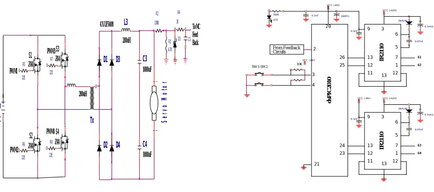
III CIRCUIT DIAGRAM
S e rv o M o to r 1 2 D3 S4 S1 L3 V in S3 Z44 R6 22E R3 4.7K S2 12V DC PWM3 Z44 D4 Z44 R2 100K C4 Z44 200uH R8 22E
4 X UF5408
D1 R4 1K 1000uF PWM4 D2 1000uF D3 C3 PWM2 Tx 200uH R7 22E C5 PWM1 R5 22E To MC Feed Back IR 2 1 1 0 20
0. 1m f
G4
3 1
VCC (+5V)
13
4. 7mf d
7
13
13
4. 7mf d
4 25
0. 1m f
2
G3
7
VC C (+5V) 0.1m f 9 23 10K G1 6 13 5 560E 21 6 26 3 12 24 10MFD G2 0.47m f 5 d sP IC 2 0 1 0 1N4148 2 2
VCC (+12V)
3
11
1N4148
9
1
VCC (+12V)
From Feedback Circuits LED IR 2 1 1 0 1 0.47m f 12 SW 1-SW2 1
VCC (+5V)
11
Fig 2 Circuit Diagram
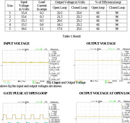
IV RESULTS AND DISCUSSIONS
Experimental results will give 100-W prototype of BB-FPC with good steady-state and dynamic performances demonstrate the feasibility and effectiveness of the proposed method with help of ANN controller.
S.no
Input Voltage in Volts
Load Current In amps
Output Voltage in Volts % of Efficiency(avg) Open Loop Closed Loop Open loop Closed Loop 1 15.4 0.2 22.0 25.6 60 96 2 15.6 0.3 21.5 25.3 60 96 3 15.3 0.5 20.0 25.2 60 96 4 15.5 0.8 18.3 25.2 60 96 5 16.0 1.0 17.6 25.0 60 96
Table 1 Result
INPUT VOLTAGE OUTPUT VOLTAGE
Fig 4 Input and Output Voltage In the above fig the input and output voltages are shown
GATE PULSE AT OPEN LOOP OUTPUT VOLTAGE AT OPEN LOOP
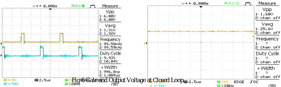
GATE PULSE AT CLOSED LOOP OUTPUT VOLTAGE AT CLOSED LOOP
Fig 6 Gate and Output Voltage at Closed Loop
The above results give better result in closed loop compare than open loop. Here we give prototype model for 12V to 24V boost converter.
V. CONCLUSION
A systematic method for synthesizing MPCs from FBC and BDCs has been proposed. The switching legs parasitized in the BDCs have been found and shared with theFBC to derive families of FB-BDC-MPCs. The proposed FBBDC-MPCs are capable of interfacing multiple bidirectional sources and isolated output load simultaneously. Single-stage power conversion between any two ports and ZVS of all the active switches have been achieved in the proposed MPCs.These result in high conversion efficiency. All the port voltages are controlled simultaneously by employing PWM and phase angle-shift control scheme. These topologies are good candidates for renewable power systems as interface converters due to their advantages of simple configuration, reduced devices, and easy control.A typical four-port converter developed by the proposed method, named as BB-FPC, is analyzed and implemented as an example, with detailed operation principles, design considerations, modulation, and power management strategies presented. Experimental results on a 100-W prototype of BB-FPC with good steady-state and dynamic performances demonstrate the feasibility and effectiveness and runs the servo drives runs at a constant speed of the proposed method.
REFERENCES
[1] H. Fakham, D. Lu, and B. Francois, “Power control design of a battery charger in a hybrid active PV generator for load-following applications,”
IEEE Trans. Ind. Electron., vol. 58, no. 1, pp. 85–94, Jan. 2011.
[2] T. Hirose and H. Matsuo, “Standalone hybrid wind-solar power generation system applying dump power control without dump load,” IEEE Trans. Ind. Electron., vol. 59, no. 2, pp. 988–997, Feb. 2012.
[3] W. Jiang and B. Fahimi, “Multiport power electronic interface—Concept, modeling and design,” IEEE Trans. Power Electron., vol. 26, no. 7, pp. 1890–1900, Jul. 2011.
[4] H. Tao, J. L. Duarte, and M. A. M. Hendrix, “Multiport converters for hybrid power sources,” in Proc. IEEE PESC, 2008, pp. 3412–3418. [5] H. Tao, J. L. Duarte, andM. A.M. Hendrix, “Three-port triple-half-bridge bidirectional converter with zero-voltage switching,” IEEE Trans.
Power Electron., vol. 23, no. 2, pp. 782–792, Mar. 2008.
[6] H. Tao, A. Kotsopoulos, J. Duarte, andM. Hendrix, “Transformer coupled multiport ZVS bidirectional dc-dc converter with wide input range,”
IEEE Trans. Power Electron., vol. 23, no. 2, pp. 771–781, Mar. 2008.
[7] K. Haribaran and N. Mohan, “Three-port series-resonant dc-dc converter to interface renewable energy sources with bidirectional load and energy storage ports,” IEEE Trans. Power Electron., vol. 24, no. 10, pp. 2289– 2297, Oct. 2009.
[8] T. Zhou and B. Francois, “Energy management and power control of a hybrid active wind generator for distributed power generation and grid integration,” IEEE Trans. Ind. Electron., vol. 58, no. 1, pp. 95–104, Jan. 2011.
[9] T. Bhattacharya, V. S. Giri, K. Mathew, and L. Umanand, “Multiphase bidirectional flyback converter topology for hybrid electric vehicles,”
IEEE Trans. Ind. Electron., vol. 56, no. 1, pp. 78–84, Jan. 2009.
[10] X. Liu, P. Wang, P. C. Loh, and F. Blaabjerg, “A compact three-phase single-input/dual-output matrix converter,” IEEE Trans. Ind. Electron., vol. 59, no. 1, pp. 6–16, Jan. 2012.
[11] R.-J. Wai, C.-Y. Lin, J.-J. Liaw, and Y.-R. Chang, “Newly designed ZVS multi-input converter,” IEEE Trans. Ind. Electron., vol. 58, no. 2, pp. 555–566, Feb. 2011.
[13] H. Matsuo, W. Lin, F. Kurokawa, T. Shigemizu, and N. Watanabe, “Characteristics of the multiple-input dc-dc converter,” IEEE Trans. Ind. Electron., vol. 51, no. 3, pp. 625–631, Jun. 2004.