Design and Implementation of an Efficient
BIST Architecture for ROM
Divya Ramachandran, Doniya Jose
M.Tech Scholar (VLSI & Embedded System), Dept. of ECE., IIET, M.G University, Kottayam, Kerala, India
Assistant Professor, Dept. of ECE, IIET, Nellikuzhy, Kerala, India
ABSTRACT: Input vector monitoring online testing schemes perform testing during the normal operation of the circuit. These schemes are evaluated based on hardware overhead and concurrent test latency (CTL), also well suited for modules requiring exhaustive testing, such as Read Only Memories (ROMs). In this work we present an input vector monitoring concurrent BIST scheme specially designed for the testing of ROM modules along with an error detecting unit which can detect error of corresponding bit position. By using circuitry already existing for the memory module, the hardware overhead, power and the delay, compared to previously proposed schemes, is significantly reduced.
KEYWORDS: Built-in-self test; testing; design for testability; circuit under test; Concurrent BIST Unit; Error detecting unit.
I. INTRODUCTION
The complexity of digital circuits has been increasing at an exponential rate with the advent of VLSI. Unfortunately, increased circuit complexity also complicates the testing problem. To make the testing easy, two new disciplines have emerged, namely, design for testability (DFT) and built-in self-test (BIST). In DFT, the extra logic is active during the test mode circuit and such logic is idle during normal operation of the circuit. BIST techniques, on the other hand, constitute a class of schemes that provide the capability of performing at-speed testing with high fault coverage, whereas simultaneously they relax the reliance on expensive external testing equipment. Thus it is an attractive solution to the problem of testing VLSI devices [8].
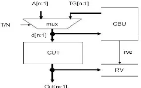
Fig. 1. Input vector monitoring concurrent BIST.
During normal mode, the vector that drives the inputs of the CUT (denoted by d[n:1] in Fig. 1) is driven from the normal input vector (A[n:1]). A is also driven to a concurrent BIST unit (CBU), where it is compared with the active test set. If it is found that A matches one of the vectors in the active test set, we say that a hit has occurred. In this case, A is removed from the active test set and the signal response verifier enable (rve) is issued, to enable the m-stage RV to capture the CUT response to the input vector [8]. When all input vectors have performed hit, the contents of RV are examined. During test mode, the inputs to the CUT are driven from the CBU outputs denoted TG[n:1]. The concurrent test latency (CTL) of an input vector monitoring scheme is the mean time required to complete the test while the CUT operates in normal mode.
In this brief, a novel input vector monitoring concurrent BIST scheme for ROM is proposed, which compares favourably to previously proposed schemes [1]–[7] with respect to the hardware overhead/CTL trade off. This brief is organized as follows. In Section II, we introduce the previous works and in Section III, the proposed scheme. In Section IV, experimental results along with the comparison of proposed scheme with the previous scheme. Finally, Section V summarizes the conclusion of this brief.
II. RELATED WORK
In [5] window-based Concurrent BIST (w-CBIST) was presented. w-CBIST has similar architecture to SRAM-based BIST. Here it is applied to the inputs of a combinational CUT with n input lines and is SRAM-based on the idea of monitoring a window of vectors, whose size is W, with W=2w, where w is an integer number w<n. Every moment, the test vectors belonging to the window are monitored, and if a vector performs a hit, the Response Verifier (RV) is enabled.
The bits of the input vector are separated into two distinct sets comprising w and k bits, such that w+k = n. The k (high-order) bits of the input vector indicate whether the input vector belongs to the window under consideration. The w remaining bits indicate the relative location of the incoming vector in the current window. If the incoming vector belongs to the current window and has not been received during the examination of the current window, we say that the vector has performed a hit and the Response Verifier is clocked in order to capture the CUT’s response to the vector. When all vectors that belong to the current window have reached the CUT inputs, we proceed to examine the next window. The scheme operates in one out of two modes, normal and test, depending on the value of the signal T/N. When T/N=0 in normal mode and when T/N =1 in the test mode.
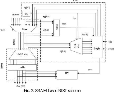
Fig. 2. SRAM-based BIST scheme.
In Fig. 2, it is case, where n = 5, k =2 and w = 3. A binary decoder will convert binary information from n input signals to as many as 2n unique output signals. The design of the decoder module for w = 3 is shown in Fig.3. The cmp is signal from comparator and tge from logic module and it operates as follows-
When test generator enable (tge) is enabled, all outputs of the decoder are equal to one.
When comparator (cmp) is disabled (and tge is not enabled) all outputs are disabled.
Fig. 3. 3x8 decoder Fig. 4. Logic module
The logic module used in the scheme is shown in Fig 4. In Fig 2, during normal mode (T/N=0) the 3 low-order inputs of the ROM are driven to a 3-to-8 decoder that addresses a 8-cell logic; the logic keeps track of whether the respective vectors have appeared to the inputs of the ROM during the examination of the current 8-vector window. The high-order input of the ROM is compared against the contents of the (2- bit) test generator to indicate whether the incoming vector belongs to the current window. During test mode, the 2-bit input vector is formed by the output of the TG and the 3-bit output of the Logic tg[3:1].
III.PROPOSED SCHEME
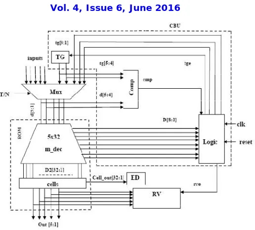
The proposed scheme exploits the decoding structure of the ROM to replace the decoder of the logic of Fig. 2. The proposed scheme exploits the internal decoder outputs to address the logic of the CBU as presented in Fig. 5. Let us consider a combinational CUT with n input lines, as shown in Fig. 2; hence the possible input vectors for this CUT are 2n.
Fig. 5. Modified SRAM-based BIST.
A. Two-Level Decoding
Decoders used in Fig. 5, commonly utilize two-level implementation. In Fig. 6, a 5-to-32 decoder implemented using two-level decoding is presented. The input d[5:4] drives a 2-to-4 decoder and its outputs are denoted as D[1.4], D[1.3], D[1.2] and D[1.1]. The low-order inputs drive a 3-to-8 decoder with outputs denoted as D[8] to D[1]. Consequently, the outputs of the 2-to-4 and 3-to-8 decoders are combined using thirty two AND gates and the outputs of the 5-to-32 decoder D2[1] to D2[32] are formed.
Fig. 6. 5-to-32 decoder with two level decoding.
B. Logic Module
The operation of the logic module is as follows: 1. Reset of the module.
2. Hit of a vector (i.e., a vector belongs in the active window and reaches the CUT inputs for the first time). 3. A vector that belongs in the current window reaches the CUT inputs but not for the first time.
4. tge operation (i.e., all cells of the window are filled and we will proceed to examine the next window).
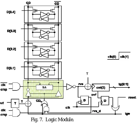
Fig. 7. Logic Module.
At the beginning of the operation, the module is reset within C cycles (where C is the number of cells), the reset takes place as follows: the external reset signal is enabled, hence the tge signal is enabled, the tg[5:1] outputs are applied to the inputs of the ROM and consequently to the D2[8] – D2[1] inputs of the cells; furthermore the CD' signal is enabled; therefore, a '1' is written to the right hand side of the cells and a '0' value to the left hand side of the cells. The initialization of the module resets the values of all SRAM-like cells to ‘0’; after that, the concurrent testing performs in odd- and even-numbered windows; the operation is as follows: during the examination of the first window, whenever a decoder output is equal to enabled and the content of the cell is equal to ‘0’, a hit is performed; therefore, a ‘1’ is written to the cell. During the examination of the second window, when a decoder output is enabled and the value of the cell is ‘1’ we have a hit and a ‘0’ is written to the value of the cell. When the examination of the second window is completed, the operation is again reversed and so on. The control of whether an odd or even window is examined is controlled by the flip flop denoted ‘T’ in Fig 7, which toggles value every time the window is full.
During normal mode, the inputs to the CUT are driven from the normal inputs. The n inputs are also driven to the concurrent BIST unit as follows: the w low-order inputs are driven to the inputs of the decoder; the k high-order inputs are driven to the inputs of the comparator. When a vector belonging to the current window reaches the inputs of the CUT, the comparator is enabled and one of the outputs of the decoder is enabled. Therefore, the following events are monitored: When a vector reaches the CUT inputs for the first time, then during the first half of the clock cycle the addressed cell is read; since the read value is 0 (in case of an odd numbered window), the w-stage counter is triggered through the NOT gate with output the rve signal. During the second half of the clock cycle, the flip flop whose clock input is inverted enables the AND gate (whose other input is clk & cmp), and enables the buffers to write the value ‘1’ to the addressed cell. Similar things happen in the case of an even-numbered window.
C. Error-Detection Unit
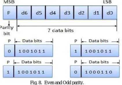
Error is a condition when the output information does not match with the input information. To avoid the occurrence of errors, we use the error-detecting codes which are additional data added to a given digital message to help us detect if an error occurred. A simple example of error-detecting code is parity check.
A parity bit, or check bit is a bit added to the end of a string of binary code that indicates whether the number of bits in the string with the value one is even or odd. Parity bits are used as the simplest form of error detecting code. There are two variants of parity bits: even parity bit and odd parity bit. In the case of even parity, for a given set of bits, the occurrence of bits whose value is 1 is counted. If that count is odd, the parity bit value is set to 1, making the total count of occurrences of 1's in the whole set (including the parity bit) an even number. If the count of 1's in a given set of bits is already even, the parity bit's value remains 0. In the case of odd parity, the situation is reversed. For a given set of bits, if the count of bits with a value of 1 is even, the parity bit value is set to 1 making the total count of 1's in the whole set(including the parity bit) an odd number. If the count of bits with a value of 1 is odd, the count is already odd so the parity bit's value remains 0.
Parity can be calculated via an XOR sum of the bits, yielding 0 for even parity and 1 for odd parity. This property of being dependent upon all the bits and changing value if any one bit change allows for its use in error detection schemes. The parity checking of error detection is the simplest technique for detecting and correcting errors. The MSB of an 8-bits word is used as the parity bit and the remaining 7 8-bits are used as data or message 8-bits.
Fig. 8. Even and Odd parity.
The parity bit can be set to 0 and 1 depending on the type of the parity required. For even parity, this bit is set to 1 or 0 such that the no. of "1 bits" in the entire word is even. For odd parity, this bit is set to 1 or 0 such that the no. of "1 bits" in the entire word is odd as in Fig. 8.
IV.SIMULATION RESULTS
The simulation studies involve the hardware overhead which is calculated using the gate equivalents as a metric. The parameters that affect the hardware overhead of the proposed scheme are n (the number of ROM inputs), m (the number of ROM outputs) and w (the window size) with k = n-w, and W = 2w. The implementation of the scheme requires the n-stage multiplexer at the inputs of the ROM, and an m-stage order independent Response Verifier. The simulation results of the SRAM –based BIST scheme in normal mode where T/N= 0 is shown in Fig. 9.
The simulation result of the SRAM-based BIST scheme in test mode is shown in Fig.10. In test mode the select input T/N=1. The test generators generate random sequence which serves as an input to the BIST.
Fig.10. Simulation result of SRAM-based BIST scheme in test mode.
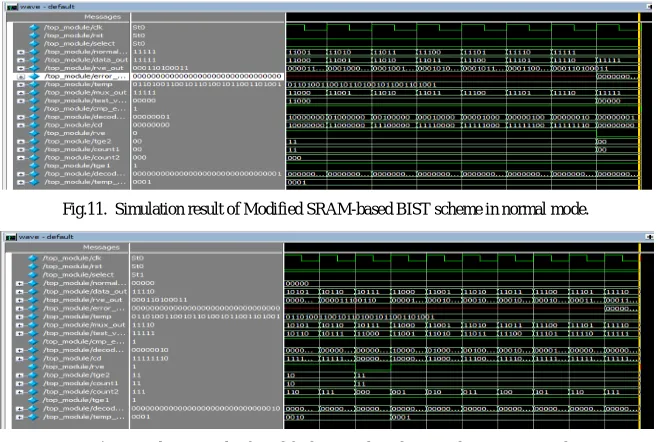
The simulation result of the modified SRAM-based BIST scheme in normal mode and test mode is shown in Fig.11 and in Fig.12. In normal mode T/N= 0 and in test mode the T/N=1. The test mode, the test generators generate random sequence which serves as an input to the BIST, whereas in normal mode the normal inputs. An error_data out, outputs a 32’b 0 when there is no error and vice versa in case of error.
Fig.11. Simulation result of Modified SRAM-based BIST scheme in normal mode.
Fig.12. Simulation result of Modified SRAM-based BIST scheme in test mode.
TABLE I. Comparison of different BIST schemes.
The comparison table is shown in table I. From the table it is clearly seen that the modified SRAM-based BIST has reduced area, delay and power consumption compared to the SRAM-based BIST scheme. The comparison chart is shown in Fig. 13, which shows the difference in area , delay, power consumption of the SRAM-based BIST and the modified SRAM-based BIST.
Design Evaluation factors
Area(no. of slices) Delay(ns) Power(W)
SRAM-based BIST
73 10.440 0.14149
Modified SRAM– based BIST
Fig.13. Comparison of Modified SRAM-based BIST scheme and previous BIST scheme.
V. CONCLUSION AND FUTURE WORK
Input vector monitoring concurrent Built-In Self-Test (BIST) schemes perform testing during the circuit normal operation without imposing a need to set the circuit off-line in order to perform the test, therefore they can circumvent problems appearing in off-line BIST techniques. In this work a novel Input vector Monitoring concurrent BIST architecture for the concurrent testing of ROMs is presented, which is shown to be more efficient than previously proposed techniques in terms of area, delay and power. Also the modified BIST has the error detecting unit which displays the error occurred in which bit position. In future we can hope to further modify it by providing some error correcting unit along with detection without compromising with efficiency.
REFERENCES
1. I.Voyiatzis, C.Efstathiou, “Input Vector Monitoring Concurrent BIST Architecture using SRAM cells”, Very Large Scale Integration (VLSI) Systems, IEEE Transactions on (Volume:22, Issue:7), Page(s):1625-1629, July 2014.
2. I.Voyiatzis, T. Haniotakis, C. Efstathiou, and H. Antonopoulou, “A concurrent BIST architecture based on monitoring suare windows”, in Proc.5th Int. Conf. DTIS, Mar 2010, pp. 1-6.
3. K. K. Saluja, R. Sharma, and C. R. Kime, “ Concurrent comparitive builtin testing of digital circuits,” Dept. Electr. Comput. Eng., Wisconsin, Madison, WI, USA,Tech.Rep. ECE8711, 1986.
4. I. Voyiatzis, A. Paschalis, D. Gizopoulos, N. Kranitis, and C. Halatsis, “A concurrent BIST architecture based on a selftesting RAM,” IEEE trans. Rel., vol. 54, no. 1, pp.6978, Mar. 2005.
5. I.Voyiatzis and C. Halatsis, “ A low cost concurrent BIST scheme for increased dependability,” IEEE Trans. Dependable Secure Comput., vol. 2, no. 2, pp.150-16, Apr.2005.
6. K. K Saluja, R Sharma, and C. R. Kime, “A concurrent testing technique for digital circuits,” IEEE Trans. Comput. Aided Design Integr. Circuits Syst., vol. 7, no. 12, pp.1250-1260, Dec. 1988.
7. M. A. Kochte, C. Zoellin, and H.-J. Wunderlich, “Concurrent self-test with partially specified patterns for low test latency and overhead,” in Proc. 14th Eur. Test Symp., May 2009, pp. 53–58.
8. E. J. McCluskey, “Built-in self-test techniques,” IEEE Design Test Comput., vol. 2, no. 2, pp. 21–28, Apr. 1985.
9. R. Sharma and K. K. Saluja, “Theory, analysis and implementation of an on-line BIST technique,” VLSI Design, vol. 1, no. 1, pp. 9–22, 1993.
10. I. Voyiatzis, “ Online testing of ROMs with input vector monitoring,” Median Workshop,2015.
BIOGRAPHY
Divya Ramachandran is an M-Tech scholar in VLSI and Embedded System in the Electronics and Communication Department, IIET, M. G. University. She received B-Tech degree in 2014 from M. G. University, Kottayam, Kerala. Her research interests are cryptography, VLSI and HDL languages etc.
Doniya Jose is an Assistant Professor in the Electronics and Communication Department, IIET, M. G. University. Her research areas are image processing, cryptography etc.
0 10 20 30 40 50 60 70 80
Area Delay(ns) Power(W)