Floating Gate FET Memory Array and Peripheral Circuits. (Under the direction of Dr. Paul Franzon).
The computation power of the portable electronic equipment like laptops, smartphones and tablets is increasing day by day. Such computing power has to be supported with a good amount of storage facility. Therefore, memory technologies like solid-state drives (SSDs) are being increasingly used as the storage device due to their density and low power consumption. However, unlike Dynamic RAMs (DRAMs) they are usually used as a source of secondary storage. The dual floating gate field effect transistor (DFGFET) has the ability to store 2 bits in a single cell. As one bit is stored in volatile state and the other in nonvolatile state, the benefits of both volatile and nonvolatile storage can be extracted from it. Therefore, it important to analyze the pros and cons of a memory array built using this device. An insight into the additional circuits required to perform various memory operations correctly in a power efficient manner is also essential. This thesis deals with these issues and presents the results obtained through circuit simulations in HSPICE. A SPICE-compatible physical model written in Verilog-A is used to model the characteristics of DFGFET in circuit simulations.
by
Abhishek Bhattacharyya
A thesis submitted to the Graduate Faculty of North Carolina State University
in partial fulfillment of the requirements for the degree of
Master of Science
Computer Engineering
Raleigh, North Carolina 2013
APPROVED BY:
_______________________________ ______________________________
Dr. Paul Franzon Dr. Brian Floyd
Chair of Advisory Committee
BIOGRAPHY
ACKNOWLEDGEMENTS
I would like to express my deepest appreciation to several people for supporting and assisting me throughout my graduate work.
First of all, I would like to thank my advisor, Dr. Paul Franzon for his guidance and constant support. He has been very patient with me. He has inspired me to put in the hard work needed for this work. I would like to express towards Dr. Gregory Byrd and Dr. Brian Floyd for supporting my research and approving to be in my advisory committee.
TABLE OF CONTENTS
LIST OF TABLES ... vi
LIST OF FIGURES ... vii
CHAPTER 1: Introduction ... 1
1.1 Motivation ... 1
1.2 Thesis Outline ... 3
CHAPTER 2: Literature Review ... 5
2.1 Overview of Existing Semiconductor Memory Technologies... 5
2.2 Volatile Memory ... 7
2.2.1 SRAM ... 7
2.2.2 DRAM... 9
2.3 Nonvolatile Memory ... 11
2.3.1 Flash Memory ... 12
2.3.2 NOR Flash Architecture ... 14
2.3.3 NAND Flash Architecture ... 15
2.4 Universal Memory Device ... 16
2.5 Modes of Operation of DFGFET ... 20
2.5.1 Volatile Mode ... 20
2.5.2 Nonvolatile Mode ... 21
2.6 Applications of DFGFET ... 23
2.6.1 Challenges in application and Potential Solutions ... 24
CHAPTER 3: Physical Model for Circuit Simulations in Spice ... 26
3.1 Basic Idea ... 26
3.2 Computation Algorithm ... 27
CHAPTER 4: Design and Power Optimization of Peripheral Circuits ... 32
4.1 Decoding Circuits ... 33
4.1.1 Row Decoder ... 34
4.1.2 Column Decoder ... 38
4.2 Column Multiplexer ... 39
4.3 Voltage drivers ... 41
4.3.1 Level-up shifter ... 41
4.3.2 Negative level shifter ... 43
4.4 Sense Amplifier ... 45
CHAPTER 5: Circuit Design and Analysis of Universal Memory Array ... 48
5.1 Universal Memory Array ... 48
5.2 Operation of the entire circuit ... 51
5.3 Results ... 57
CHAPTER 6: Conclusion and Future Work ... 60
6.1 Conclusion ... 60
6.2 Future Work ... 61
LIST OF TABLES
Table 2.1: Classification of Semiconductor Memory Technologies ... 6
Table 2.2: Comparison between Flash memory and other nonvolatile memory alternatives . 12 Table 4.1: MOSFET sizes in row decoder (nm) ... 37
Table 4.2: MOSFET sizes in level-up shifter (µm) ... 42
Table 4.3: MOSFET sizes in sense amplifier (nm) ... 47
Table 5.1: Wire parameters used in parasitic extraction ... 50
Table 5.2: Parasitic Resistance and Capacitance of bit line and word line ... 51
Table 5.3: States of a universal memory array cell before and after applied voltage envelope for various operations ... 54
LIST OF FIGURES
Figure 2.1: 6T SRAM cell ... 8
Figure 2.2: 1T DRAM cell ... 9
Figure 2.3: Cross-section of a flash device ... 13
Figure 2.4: Circuit organization of NOR Flash ... 14
Figure 2.5: Circuit organization of NAND Flash ... 15
Figure 2.6: Cross-section and doping profile of 16 nm universal memory device ... 16
Figure 2.7: Band diagram across the gate stack under flat-band condition ... 18
Figure 2.8: Id-Vg curves of the four states of the universal memory device (Dyn=Dynamic state; NV= Nonvolatile state) ... 19
Figure 3.1: Spice compatible physical model ... 26
Figure 3.2: Capacitance model of universal memory device ... 27
Figure 3.3: Band diagram of DFGFET in (a) program mode, (b) erase mode ... 29
Figure 3.4: Flowchart for the computation process of the physical model ... 30
Figure 4.1: Schematic of the first stage of the pre-decoding scheme ... 34
Figure 4.2: Schematic of the second stage of the pre-decoding scheme ... 35
Figure 4.3: Waveforms for the output lines (L0-L3) for different input addresses of row decoder ... 37
Figure 4.4: Schematic of column decoder ... 39
Figure 4.5: Schematic of column multiplexer... 40
Figure 4.6: Level-up shifter ... 41
Figure 4.7: Simulated waveforms of level-up shifter ... 42
Figure 4.8: Conventional negative level shifter ... 43
Figure 4.9: Schematic of negative level shifter ... 44
Figure 4.10: Simulated waveforms of negative level shifter ... 45
Figure 4.11: Sense amplifier ... 46
Figure 4.12: Timing diagram showing sense amplifier operation ... 47
Figure 5.1: Universal memory array ... 48
Figure 5.2: Model of bit line and word line in Q3D Extractor ... 50
Figure 5.3: Top-level schematic of write circuit ... 53
Figure 5.4: Top-level schematic of read circuit ... 52
Figure 5.5: Waveforms for dynamic read from HSPICE simulations ... 58
CHAPTER 1 Introduction
This chapter explains the motivation behind the research work done on design and power optimization of a 16 nm dual floating gate memory array and the peripheral circuits. The latter part of the chapter presents a brief outline of the thesis organization.
1.1 Motivation
thereby producing a shift in the threshold voltage. The different amounts of charge trapped in the two floating gates results in different shifts in the threshold voltage, and these shifts are used to identify the volatile and the nonvolatile states of the memory cell. As this makes it possible to save data in the main memory, thereby enabling instant-on computing, energy efficiency is achieved. Moreover, a memory access speed comparable to that of dynamic RAM is maintained.
array in order to avoid the larger time involved in accessing the NAND type array due to its cascaded nature. Besides, NOR type architecture is closer to the reference DRAM architecture. The circuit designs are done in Cadence Virtuoso using Daniel Schinke’s Verilog-A file for creating the library for the universal memory device, and the simulations are run in HSPICE.
1.2 Thesis Outline
The literature review in chapter 2 gives an overview of existing volatile and nonvolatile memory technologies and discusses the basic structure, operating principle, applications and design challenges of the dual floating gate device.
For circuit level investigations the surface potential based physical model presented by Daniel Schinke is tweaked for 16 nm and used. This model is compatible with the existing SPICE-based infrastructure. Chapter 3 discusses the physical model in detail. The model involves an iterative algorithm that makes the computation fast enough to be suitable for circuit simulations in SPICE.
Chapter 5 describes the application of the universal memory device in a memory sub-array (128 x 128) as storage elements. This enables instant-on computing as it allows the array to switch between active mode and hibernation, and vice versa, quickly. This chapter explains the read and the write operations of the memory array and gives an account of the power consumption involved. In addition, the field solver model built in Q3D for the bit lines and the word lines and the parasitic extraction values obtained from it are presented.
CHAPTER 2 Literature Review
This chapter gives an overview of existing volatile and nonvolatile memory technologies and presents in detail the basic structure, operating principle, applications and design challenges of the dual floating gate device. Towards the end of the chapter, the changes made in the 16 nm dual floating gate device to reduce leakage currents and obtain steeper Id-Vg curves are explained.
2.1 Overview of Existing Semiconductor Memory Technologies
Semiconductor based memories are an integral part of today’s integrated circuits and they continue to dominate the overall memory market. It has been one of the greatest driving forces in the advancement of solid state technology which has supplanted the heavier magnetic hard drives in personal computers as well as in servers. Semiconductor based memories account for roughly 20-25% of the overall semiconductor industry market [3]. The current market size of semiconductor memory is around 60 billion USD and it is estimated to grow beyond 90 billion USD by 2017. This can be attributed to the fact that semiconductor based memories have faster access speeds and higher storage density. Furthermore, since they are less heavy and less power hungry they are an obvious choice for mobile devices.
fall into this category. Nonvolatile memory can retain data even if the power is off. The classification of the various types of semiconductor memory is shown in Table 2.1 [4].
Table 2.1: Classification of Semiconductor Memory Technologies [4] Volatile Memory
(RAM)
SRAM Asynchronous SRAM
Synchronous SRAM
DRAM Asynchronous DRAM
Synchronous DRAM SDRAM
DDR/DDR2/DDR3 DRAM XDR DRAM Nonvolatile Memory (ROM) Mask ROM Programmable ROM OTP ROM EPROM EEPROM
Flash ROM NOR type
NAND type
programmable floating gate embedded in the dielectrics between the control gate and the silicon substrate.
2.2 Volatile Memory
The two most widely used volatile memories are SRAM and DRAM. Volatile memories lose their data when the power is off. In other words, they need a constant supply of power to hold the information saved. As soon as the power supply is cut off the data held by these memories get corrupted or completely lost. Since volatile memories enable faster read and write they find application primarily as quick access but temporary storage media. Two such applications are cache and main memory. Caches hold a small but repeatedly accessed portion of the main memory by the program running currently in the processor. The main memory is the next faster option after the caches, but is denser in terms of bits stored. The structure of the basic storage units (bit cells) and operation principle of these two types of volatile memories are elaborated in the next subsections.
2.2.1 SRAM
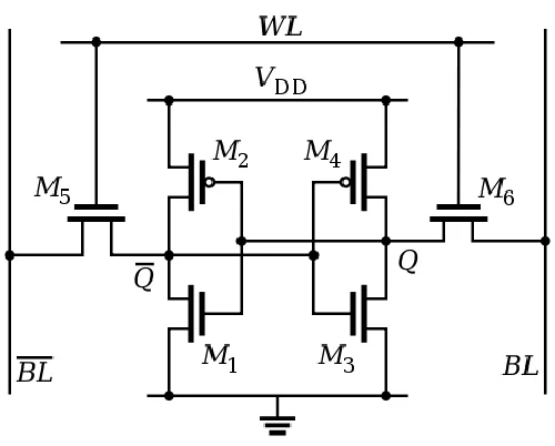
Static random access memory (SRAM) is a high speed, randomly accessible volatile memory. Figure 2.1 shows the bit cell of a typical 6T SRAM composed of two PMOS and four NMOS transistors. The transistors (M1-M4) form a positive feedback cross-coupled
the cell for reading and writing. Bit lines BL and BL access data in and out of the cell via M6
and M5 respectively. These word lines and bit lines extend and connect several bit cells into
rows and columns respectively. The data is retained with the help of the cross-coupled inverters while the power supply is on and the transistors that are on are either connected to the supply or the ground. Hence, SRAM operates on the principle of static logic and is a volatile memory.
Figure 2.1: 6T SRAM cell
DRAM is usually used for main memory for reasons that will be discussed in the next subsection.
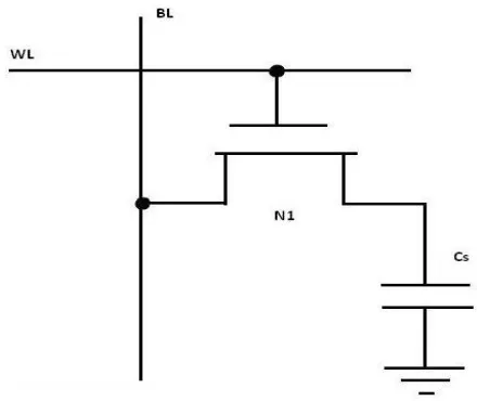
2.2.2 DRAM
DRAM stores data by dint of a storage capacitor (Cs). A typical DRAM cell consists
of a single transistor as illustrated in Figure 2.2. The word line (WL) is connected to the gate terminal of the NMOS transistor N1 and the bit line (BL) is connected to its drain. The word line is pulled high to read from or write into the cell and pulled low to isolate it. The bit line is used to access the data stored in the bit cell. The word lines and the bit lines extend to connect other cells into rows and columns respectively. The bit lines are connected to sense amplifiers that sense and read out the data stored in the selected bit cell.
Unlike an SRAM cell, the charge stored in the storage capacitor in a DRAM cell leaks away gradually when it is idle. Therefore, DRAM cells need periodic refresh to maintain their data. According to the JEDEC standards, all rows in a DRAM require a refresh at least every 64 ms [2]. This adds to their power consumption.
For writing into a DRAM cell, the word line is pulled high to activate the transistor N1 and store a “1” or a “0” in the storage capacitor. But first, the bit line is pre-charged to VDD to write logic 1 or it is pre-discharged to ground to write logic 0.
During read, firstly, the bit line is pre-charged to a predetermined voltage level between ground and VDD, usually VDD /2. In the second half of the read cycle, the pre-charge
Due to its 1T configuration DRAM is typically used as main memory in CPUs as it has higher storage density that reduces the cost per bit significantly. They are not suitable for caches since they have slower writes and larger power consumption.
2.3 Nonvolatile Memory
2.3.1 Flash Memory
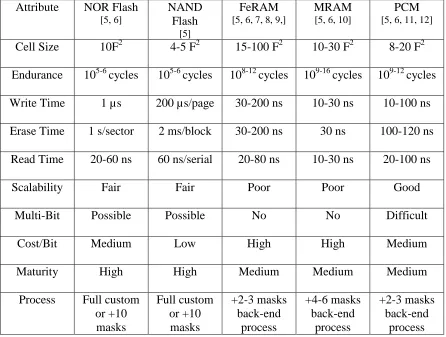
Flash memory was invented by Dr. Fujio Masuoka while he was working for Toshiba [24]. He and his colleagues presented the invention at IEDM in 1984. One of the reasons of the wide acceptance of flash memories is their compatibility with CMOS process. As the basic structure and the operating principle of the flash memory device are similar to that of the universal memory device, its structure and operation are described in the next few paragraphs.
Table 2.2: Comparison between Flash memory and other nonvolatile memory alternatives Attribute NOR Flash
[5, 6]
NAND Flash
[5]
FeRAM [5, 6, 7, 8, 9,]
MRAM [5, 6, 10]
PCM [5, 6, 11, 12]
Cell Size 10F2 4-5 F2 15-100 F2 10-30 F2 8-20 F2 Endurance 105-6 cycles 105-6 cycles 108-12 cycles 109-16 cycles 109-12 cycles Write Time 1 µs 200 µs/page 30-200 ns 10-30 ns 10-100 ns Erase Time 1 s/sector 2 ms/block 30-200 ns 30 ns 100-120 ns
Read Time 20-60 ns 60 ns/serial 20-80 ns 10-30 ns 20-100 ns
Scalability Fair Fair Poor Poor Good
Multi-Bit Possible Possible No No Difficult
Cost/Bit Medium Low High High Medium
Maturity High High Medium Medium Medium
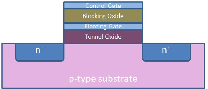
Flash transistors are similar in composition to MOSFETs except they have a floating gate interposed between the control gate and the substrate. The floating gate is surrounded by an oxide layer on all sides. Due to this electrical insulation, known as Schottky barrier formation, the charges trapped on the floating gate via tunneling take many years to get discharged. The charges trapped on the floating gate partially screen the electric field from the control gate and produces a shift in the threshold voltage of the transistor. The operating principle of the universal memory device discussed in this thesis is largely based on this premise. The structure of a typical flash device is illustrated in Figure 2.3.
Figure 2.3: Cross-section of a flash device
memories have storage density, long retention capability and low power consumption that make it fit for use as a secondary storage device. Devices like flash drives, solid state drives (SSD), etc. are examples of commercially available forms of flash memory.
2.3.2 NOR Flash Architecture
Figure 2.4: Circuit organization of NOR Flash
applying a high voltage supply. An opposite supply is applied and the device is erased through Fowler- Nordheim Tunneling (FNT). Typically, the memory chip is hierarchically divided into multi-level sub-arrays, namely pages, sectors and blocks, instead of having a single large memory array. NOR Flash technology has low read latencies. This characteristic of NOR devices allow for both direct code execution and data storage in a single memory product. Thus, NOR flash has been the technology of choice for embedded applications requiring a discrete non-volatile memory device.
2.3.3 NAND Flash Architecture
Figure 2.5: Circuit organization of NAND Flash
connected to the source line and is used as a ground select transistor. The transistors are connected in series, and only if all word lines are pulled high is the bit line pulled low. Despite the additional transistors, the reduction in ground wires and bit lines allows a denser layout and greater storage capacity per chip. This reduces the cost per bit also. However, the cascaded connection of the transistors renders it slow. The life span or endurance of a NAND flash is greater than that of a NOR flash. This is a consequence of the fact that program as well as erase operations in NAND flash are done through Fowler-Nordheim Tunneling only. The stress on the oxide, as such, is less and breakdown is slower. Therefore, NAND flash is primarily used as secondary memory storage devices like flash drives and SSDs.
2.4 Universal Memory Device
The cross-section of universal memory device in 16 nm technology is shown in Figure 2.6 [2]. The structure is very similar to a MOSFET, but it has two metal floating gates interposed between the control gate and the substrate. Thus, it is also called dual floating gate device (DFGFET). The DFGFET shown in the figure is an SOI-based device with a thin oxide and a back gate at the bottom of the substrate. The primary purpose of the back gate is to enable selection of a device for operation like program and erase. As shown in Figure 2.6, the universal memory device reported by Schinke et al. has a control gate (CGate) and a back gate (BGate) composed of molybdenum with thickness 50 nm and 10 nm respectively. The top floating gate (FGTOP) is made of platinum and the bottom floating gate (FGBOT) is made
of magnesium, although both have the same thickness of 3 nm. One major issue with scaling of the device is drain-induced barrier lowering (DIBL). Thus, an SOI substrate is used for the device. The dielectric oxide between the bottom floating gate and the SOI substrate, also called bottom oxide or tunneling oxide (OX1), is composed of SiO2 and has a thickness of 4
nm. There is a dielectric barrier between the two floating gates made of HfSiO. It is called middle oxide or inter-floating gate oxide (OX2) and is 3.2 nm thick. The dielectric between
the control gate and the top floating gate is called top oxide or blocking oxide (OX3). It is
made of HfO2 and has a thickness of 18 nm. There is an oxide layer at the bottom of the
substrate that separates the back gate from it. It is called back gate oxide (OXBG) and is made
of SiO2 with thickness of 1.2 nm. The doping concentration of source/drain regions, which
The basic principle of operation of the universal memory device is similar to that of a flash device. Charges are trapped in the floating gates by quantum tunneling and a shift in the threshold voltage is produced. The polarity of the charge trapped in the floating gates determines whether the threshold voltage of the charged device is greater or less than that of an uncharged device. The amount of charge determines the magnitude of the shift. The novel idea of using two floating gates to trap charges enables this device to operate as both fast volatile storage and persistent, power efficient nonvolatile storage at the same time. The energy band diagram across the device layers under flat-band condition is shown in Figure 2.7 [2].
Figure 2.7: Band diagram across the gate stack under flat-band condition [2]
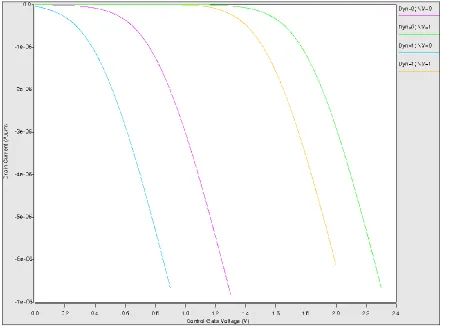
voltage. Figure 2.8 illustrates the Id-Vg curves of the different states of universal memory device and the respective shifts in threshold voltage with respect to an uncharged device (state “00”).
2.5 Modes of Operation of DFGFET
As discussed previously, there are two modes of operation in a universal memory device, volatile and nonvolatile. They are quite independent of each other. Programming and erasing the device for this 2-bit operation requires different amount of voltages and time. The tunneling effects are also different due to different electric fields across the device. A brief discussion of these two modes follows in the next subsections.
2.5.1 Volatile Mode
A dual floating gate device can be programmed by applying a positive voltage across the gate stack, i.e. control gate voltage should be greater than back gate voltage. For programming in dynamic mode the applied voltage should be sufficient to cause tunneling of electrons between the floating gates and not from the channel to the floating gates. The tunneling currents through the inter-floating gate oxide lead to rapid charge redistribution between the floating gates. As a result, equal but opposite charges accumulate in them. As the control gate voltage is positive, the top floating gate gets positively charged and the bottom floating gate gets negatively charged. Since the bottom floating gate is closer to channel than the top floating gate, it has a stronger influence on the I-V characteristics of the device. Thus, the positive charges on the bottom floating gate produce a negative threshold voltage shift (~ -330 mV) with respect to uncharged device [2]. This shift can be sensed by a sense amplifier as dynamic state of the device.
inter-floating gate oxide once the supply is off. As a result, the device needs periodic refresh similar to DRAM in order to retain correct data. The high work function top floating gate significantly slows down the charge leakage and improves the dynamic retention.
Erase operation requires that a negative voltage is applied across the gate stack. The basic operating principle is similar to dynamic programming. However, the charges flow in the opposite direction in this case. Erasing the dual floating gate takes significantly longer time than programming. This is because of the high energy barrier the electrons have to overcome while tunneling from the top floating gate to the bottom floating gate [2].
The voltages applied in dynamic mode to program or erase the device are low. As such the electric fields are low and uniform (<0.2 V/nm) and direct tunneling is the dominant type of tunneling under this conditions. Thus, the damage to the inter-floating gate oxide is much less and endurance of the device is high [2].
2.5.2 Nonvolatile Mode
Injection. The tunneling currents through the inter-floating gate oxide lead to rapid charge redistribution between the floating gates.
the uncharged device is produced due to the increased negative polarity of the bottom floating gate [2].
The operational principle of nonvolatile erase is similar to nonvolatile programming, except that the charges flow in opposite direction. A relatively a high negative voltage is applied across the gate stack for a long duration (few μs). The energy barrier between top floating gate and middle oxide is higher than that between bottom floating gate and bottom oxide. Therefore, it is easier to tunnel electrons from the bottom floating gate tunnel back to the channel than from the top floating gate to the bottom floating gate. The duration of erase depends on the time needed to achieve net charge of zero on the floating gate pair. When the supply is removed the device returns to its uncharged state after the non-volatile erase followed by charge settling after some time (~1 s).
2.6 Applications of DFGFET
DFGFET can store two bits independently, i.e. one in volatile state and another in nonvolatile state. This enables the device to support instant-on computing. This means when a computer is idle, the entire volatile memory is quickly copied to nonvolatile memory so that it can go into hibernation and switched back to active mode instantly when required.
The 2 bit operation of DFGFET facilitates fast check-pointing which considerably improves fault tolerance and recovery of CPUs. The non-volatile memory mode of universal memory array can be used to take quick back-up of the volatile mode; this application is called check-pointing. The check-pointing can be taken either in regular intervals or on detection of transient fault or upon power-down [2].
DFGFET also finds application in network-on-chips (NoCs), especially to make “just in time” networks wherein a circuit path is setup in advance of a packet transmission and torn down later. Since in volatile mode of operation the device is quite fast, it can be used as JIT circuit switch for NoCs. This enables routing information to be sent ahead of the packet(s). The unused switches can be easily turned off by switching to the nonvolatile charged state the device, thereby saving power consumption due to leakage currents.
2.6.1 Challenges in application and Potential Solutions
Daniel Schinke
pointed out several challenges in application of DFGFET andsuggested a few potential solutions in his dissertation [2]. They are discussed below:
Endurance requirements: DFGFET has high endurance in volatile mode (up to 106 cycles) [2]. However, in nonvolatile mode as well, good endurance is desirable. This would make load remapping schemes easier to implement. Potential ways to improve endurance over flash device standards are as follows:
Use of direct tunneling in the dynamic memory mode: As direct tunneling
Lower voltages and electric fields: To reduce oxide stress lower voltages
should be used for read/write and erase operations.
Discontinuous floating gates: Use of discontinuous floating gates like
nano-crystals may improve endurance of the device, as its susceptibility to SILC may be reduced.
Robust dielectrics: Trap-free dielectrics can be used to lengthen life.
Tradeoff between dynamic erase and retention times: To achieve a longer retention time two metal gates one of which has low work function and the other high work function can be employed. However, this would lead to slower dynamic erase compared to dynamic retention time. If two low work function metal floating gates are used, dynamic erase can be made faster. But the dynamic retention time will suffer. Using a thicker inter-floating gate oxide with a high electron affinity and a narrow band gap may improve both dynamic retention and dynamic erase due to the reduced barrier height.
CHAPTER 3
Physical Model for Circuit Simulations in Spice
3.1 Basic Idea
The concept that is used for the physical model of the universal memory device is shown in Figure 3.1 [2]. The block diagram consists of a Verilog-A module of the behavioral model of the device, which is connected to a Predictive NMOS transistor [13, 14]. The
physical model is based upon the assumption that the floating gate of the device can be
treated as the gate of a traditional MOS device with very similar effects from the point of
view of typical MOS characteristics, as in continuous floating gate devices. Therefore, the
bottom floating gate and threshold voltage of the universal memory device replace the gate
and threshold voltage of a MOS transistor [2].
Figure 3.1: Spice compatible physical model [2]
The control gate voltage VCG is the input for the Verilog-A module. The output is
of a Predictive NMOS transistor in order to obtain the correct I-V characteristics [13, 14]. The module models all the physical behaviors of the device. Apart from programming and erasing of the device, it takes care of the fact that the voltage on the floating gate VBFG needs
to be dynamically refreshed with respect to time, such that charge leakage and unintended programming during operation mode is included. The voltage is then applied to the gate terminal of any SPICE compatible NMOS transistor model, which is designed with an oxide thickness equal to the tunnel oxide thickness tox1 of the universal memory device in order to
obtain the correct I-V characteristics [2]. The Verilog-A module consists of a set of iterative analytical equations based on quantum tunneling with no correction factors or curve fitting that rapidly computes the charges on the metal floating gates. The device structure from Figure 2.6 of Chapter 2 serves as the reference model for this physical model.
3.2 Computation Algorithm
The capacitance model of the universal memory device is illustrated in Figure 3.2 [2]. C1 is the capacitance formed by the control gate and the top floating gate with the top oxide as the dielectric. C2 is the capacitance formed by the top floating gate and the bottom floating gate with the middle oxide as the dielectric. Similarly, C3 is the capacitance formed by the bottom floating gate and the silicon substrate with the bottom oxide as the dielectric. The figure also shows the tunnel current densities for each oxide in both vertical directions. The direction of the tunnel currents depend on the control gate voltage VCG and the charges
on the floating gate pair. The tunnel current density into each floating gate is the difference between the inward and the outward tunnel current densities, and given by
JFG_BOT = Jin,FG_BOT – Jout,FG_BOT (3.1)
JFG_TOP = Jin,FG_TOP – Jout,FG_TOP (3.2)
where the values of inward and outward current densities are independently calculated as Jin,FG_BOT = Jin,sub-FG_BOT + Jout,FG_BOT-FG_TOP (3.3)
Jout,FG_BOT = Jout,sub-FG_BOT + Jin,FG_BOT-FG_TOP (3.4)
Jin,FG_TOP = Jin,FG_BOT-FG_TOP + Jout,FG_TOP-CG (3.5)
Jout,FG_TOP = Jout,FG_BOT-FG_TOP + Jin,FG_TOP-CG (3.6)
The current equations are governed by direct tunneling and Fowler-Nordheim tunneling principles (not shown here). The barrier heights b at the Si/SiO2, Mg/HfSiO, and
Pt/HfO2 interfaces that are essential for the program mode are chosen by b,Si/SiO2 = 3.15 eV, b,Mg/HfSiO = 1.25 eV, and b,Pt/HfO2 = 2.75 eV, respectively. In the erase mode, the barrier
eV, b,Pt/HfSiO = 3.1 eV, and b,Mg/SiO2 = 2.9 eV, respectively. The effective electron mass in
the HfSiO insulator is chosen to be 0.2m0 [15, 16] and in the HfO2 insulator 0.17m0 [17],
where m0 is the free electron mass. It is important to note that this model is completely
parameterized in terms of process and geometry; thus it can be configured according to performance needs [2]. As the direct tunneling and Fowler-Nordheim tunneling equations are dependent on the electric fields and voltages across each insulator, they need to be computed. Figure 3.3 (a) and (b) show the band diagram of the device when the device is in program mode and erase mode, respectively [2]. The equations for electric fields and hence, voltages can be derived from this figure. The voltage drops across the tunnel or bottom oxide V1, inter
floating gate or middle oxide V2, and control gate or top oxide V3 are then given by
V1 = |VFG_BOT – Vsurface| (3.7)
V2 = |VFG_BOT – VFG_TOP| (3.8)
V3 = |VCG + φm – VFG_TOP| (3.9)
where φm represents the contact potential between the control gate and the control gate oxide.
After determining the tunnel current densities, the new charge on the bottom floating gate QFG_BOT and top floating gate QFG_TOP after one time step Δt can be computed by
summing together the charge of the previous time step and the additional charge during the current time step:
QFG_BOT = QFG_BOT_prev + JFG_BOTAreaFG_BOTΔt (4.0)
QFG_TOP = QFG_TOP_prev + JFG_TOPAreaFG_TOPΔt (4.1)
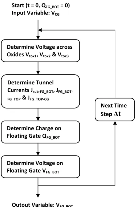
Figure 3.4: Flowchart for the computation process of the physical model
Determine Voltage across Oxides Vtox1, Vtox2 & Vtox3
Determine Tunnel Currents Jsub-FG_BOT, J FG_BOT-FG_TOP & JFG_TOP-CG
Determine Charge on Floating Gate QFG_BOT
Determine Voltage on Floating Gate VFG_BOT
Next Time Step Δt Start (t = 0, QFG_BOT = 0)
Input Variable: VCG
The final step is to update the voltages on the floating gate pair with values from equations 4.0 and 4.1. Note that VFG_BOT and VFG_TOP are interdependent, as the value of
VFG_BOT from the previous time step is used in computing VFG_TOP at the current time step:
VFG_TOP = (VCG + φm) C3 + VFG_BOTC2/C2 + C3 + QFG_TOP/C2 + C3 (4.2)
VFG_BOT = VFG_TOPC2 + VsurfaceC1/C1 + C2 + QFG_BOT/C1 + C2 (4.3)
VFG_BOT is then the output of the Verilog-A module and drives the gate of the
CHAPTER 4
Design and Power Optimization of Peripheral Circuits
The circuit design and power analysis of the memory array in 45 nm technology is reported in Daniel Schinke’s dissertation [2]. With the IC industries rapidly moving ahead and feature size reduced to technologies smaller than 45 nm, it is necessary to scale down the memory array to a smaller technology node. As such, the memory array is scaled down to 16 nm and an insight of the related design issues is presented in this thesis. Moreover, the design presented by Daniel Schinke [2] only consisted of the memory array. The peripheral circuits required for carrying out the memory operations like read, write and refresh are not discussed.
circuits, except for the line drivers, were built in 16 nm technology using Predictive MOSFET models from Arizona State University [13, 14].
4.1 Decoding Circuits
4.1.1 Row Decoder
There are two types of dynamic decoders: NOR and NAND decoders. In a NOR decoder all the output nodes except the one selected is discharged. The selected output node remains at the pre-charge voltage value. Thus, NOR decoders have a drawback of large charging and discharging power. The power increases with larger memory arrays because of the increased number of nodes. On the other hand, NAND decoder allows the selected output node to be discharged, while leaving the remaining output nodes at their pre-charge voltage values. CMOS decoders are preferred over NMOS decoders because the discharging power in the former is independent of memory capacity. Thus, dynamic NAND decoder is selected for the memory array circuit.
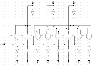
However, NAND decoders suffer from the drawback of slow speed due to a node being discharged by stacked transistors. To mitigate this performance issue a two stage decoding scheme is used. Figure 4.1 shows the schematic of the first stage of the pre-decoding scheme. The circuit is composed of eight 3 input NAND gates. The output node of one of the NAND gates is pulled low, depending on the various states of the inputs A, B and C, i.e. from state “000” to state “111”. The output nodes of the remaining NAND gates remain high. The CMOS inverters connected to the output nodes of the NAND gates are used to invert the outputs from this stage, so that they can be applied correctly as inputs to the second pre-decoding stage. For instance, if all the inputs A, B and C are high, then the output node o_7 is driven high.
Figure 4.2: Schematic of the second stage of the pre-decoding scheme
four pairs of input lines, one each from the two input blocks, are formed and fed to 64 two input NAND gates. The output nodes of the NAND gates are again inverted through CMOS inverters for the next circuit.
A pre-decoding scheme achieves a faster decoding and area reduction of a decoder. In addition, the number of stacked transistors in a NAND CMOS decoder is also reduced. Due the two staged pre-decoding scheme, the final decoder circuit has only two NMOS transistors connected in series to pull down each output node. There is an additional NMOS transistor connected in series to connect the output node to ground when charge is off. During pre-charge all the 128 output nodes are pre-charged to 1 V (VDD) via PMOS transistors. During
decoding pre-charge is off and the output nodes other than the selected node are floating high. As such, charge sharing occurs between the unselected output nodes and the gate-source capacitance of NMOS transistors connected to those nodes. Although the transistors used in the circuit are 16 nm in size and the amount of charge sharing is not much, it certainly adds to the power dissipation. So, a 45 nm PMOS transistor is connected between VDD and the source terminal of the PMOS transistors and its gate terminal is connected to
Table 4.1: MOSFET sizes in row decoder (nm)
Component NMOS (W/L) PMOS (W/L)
3 input NAND 64/16 (3*), 128/16 (1) 160/16 (1) 2 input NAND 32/16 (2), 96/16 (1) 96/16 (1)
Inverter 32/16 (1) 64/16 (1)
Main decoding circuit 32/16 (131) 64/16 (128)
* The numbers shown in brackets indicate the number of transistors of that size
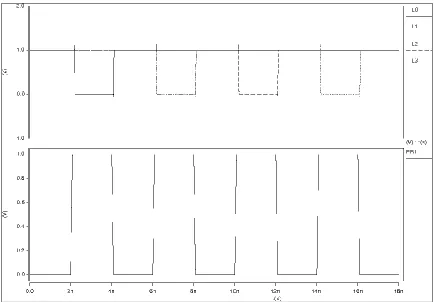
Figure 4.3 manifests the waveforms for the output lines (L0-L3) from HSPICE simulations. As evident from the figure, when PR! is low (during pre-charge) all the output lines are pulled high. When pre-charge is off each output line is pulled low depending on the address bits at the input of the decoder, i.e. L0 is pulled down to ground when the address bits (a7-a13) are all zero, representing row address “0”. Similarly, L1-L3 are pulled low corresponding to the input bits (a7-a13) representing row address “1”-“3”.
4.1.2 Column Decoder
Figure 4.4: Schematic of column decoder
4.2 Column Multiplexer
the gate terminal of the transistors. When an output node (S0, S1, S2…etc.) goes low the corresponding PMOS transistor gets activated and conducts the current from the bit line (L0, L1, L2…etc.) connected to its drain terminal. The multiplexer selects only 1 input bit line out of 16 at a time. It selects between bit lines, spaced 8 lines apart, i.e. L0 is connected to BL0, L1 to BL8, L2 to BL16, and so on. This is done to make sure there is a uniform delay to read a byte and position of bit cells from the row decoder does not affect read access time. There are 8 such multiplexers in total that select an output of 1 byte (8 bits).
4.3 Voltage drivers
To program and erase, the universal memory array has to apply high positive and negative voltages on the word lines. As such, one up shifter for write and one level-down shifter for erase are selected and modified for the purpose of driving the word lines of the memory array. These shifters consist of large 3.3 V zero-Vt transistors, a standard MOSFET in a 0.18 µm dual gate oxide CMOS process. Hence, no extra process is required. SPICE models used for circuit simulations are based on BSIM3 model.
4.3.1 Level-up shifter
The level-up shifter chosen for driving the word lines during write is shown in Figure 4.6 [18]. Zero-Vt 3.3 V NMOS transistors NA1 and NA2 are used to protect 1V NMOS transistors from high voltage stress. NA1 (NA2) is off when P1 (P2) pulls up node O1 (O2). Thus, the parasitic capacitance of N1 (N2) is isolated from the high voltage stress. N3 and N4 are added to provide further protection and their gate terminals are fixed to VDD.
Table 4.2: MOSFET sizes in level-up shifter (µm)
MOSFET Size
NA1, NA2 20/0.45
N1, N2, N3, N4 2/0.05
P1, P2 1/0.45
MOSFETs used in the level-up shifter circuit are listed in Table 4.2 adjacent to their sizes. P1 and P2 are low-Vt 3.3 V PMOS transistors.
Figure 4.7 shows the simulated waveforms at nominal temperature of 25ºC with VDDQ = 7 V and VDD = 1 V. Level-up transition from 0 V to 7 V takes about 2.8 ns.
4.3.2 Negative level shifter
The conventional negative level shifter shown in Figure 4.8 [19] consists of a cross-coupled pair of NMOS transistors MN1 and MN2. Thus, it has a differential output pair at nodes A and B. When the output B gets pulled high to VDD, then the opposite NMOS transistor will be switched on, and the output on node A will be pulled down to negative voltage VN and vice-versa.
Figure 4.8: Conventional negative level shifter [19]
circuit used for this thesis so that it can switch to 0 V rather than to VDD. To cope with the high negative voltages used in this circuit zero-Vt 3.3 V NMOS and low-Vt 3.3 V PMOS transistors are used. However, unlike the level-up shifter mentioned in Section 4.3.1, they are used as pull-up and pull-down devices in the negative level shifter. The schematic of the modified negative level shifter circuit is shown in Figure 4.9.
Figure 4.9: Schematic of negative level shifter
Figure 4.10 shows the simulated waveforms at nominal temperature of 25ºC with VDD = 1 V and VN = -7 V. Transition from 0 V to -7 V takes about 3.2 ns.
Figure 4.10: Simulated waveforms of negative level shifter
4.4 Sense Amplifier
require a smaller voltage difference to sense the data out from the bit cell. The sense amplifier shown in Figure 4.11 operates in three phases: pre-charge, signal amplification and reset.
Figure 4.11: Sense amplifier
The sense amplifier is enabled by turning on Switch Men. During the pre-charge phase, M7 is on and equalizes the output node voltages Va and Vb. If Icell > Iref, a larger
current flows through M5 than M6 (IM5 > IM6). As a result, the bias at node cin is slightly
higher than that at rin. M3 and M4 are sized so that they remain in the saturation region and
so the gate to source voltage (Vgs) of M3 is less than that of M4 (Vgs3 <Vgs4). This in turn
makes the current through M3 smaller than that of M4 (IM3 < IM4). M7 is turned off when
feedback amplifier and hence, the impedance looking into the source node of either M3 or M4 is negative. Thus, when M7 is turned off M3 and M4 begin to source the currents. As Vgs3 < Vgs4,M4 has stronger ability than M3 does to pull down node b. The different currents
flowing through the drains of transistors M3 and M4 amplify the voltage difference across the output nodes (a and b) of the sense amplifier. The timing diagram illustrating the operation of the sense amplifier is shown in Figure 4.12 [20]. Table 4.3 lists the sizes of the MOSFETs in the circuit.
Figure 4.12: Timing diagram showing sense amplifier operation
Table 4.3: MOSFET sizes in sense amplifier (nm)
MOSFET Size
M1, M2 64/16
M3, M4, M7, Men 32/16
CHAPTER 5
Circuit Design and Analysis of Universal Memory Array
5.1 Universal Memory Array
Figure 5.1: Universal memory array [2]
voltage Vref. The overall structure of the memory array is similar to that of a NOR Flash. The
resistor RBL and capacitor CBL for each bit line represent the wire resistance and capacitance,
respectively. DFGFET can store two bits, by having one bit stored in a dynamic state, while keeping another bit stored in the nonvolatile state. Each combination of bits is detected by using the sense amplifier discussed in the previous chapter by performing two successive reads.
The values for bit line wire resistance and capacitance RBL and CBL for each column
and the word line wire resistance and capacitance RWL and CWL (not shown in Figure 5.1) are
calculated using the field solver tool Q3D Extractor from Ansys for read and write separately. A frequency of about 1 GHz was assumed for read and a frequency of about 33.34 MHz was assumed for write. A simple model was built using the tool, a section of which is shown in Figure 5.2. The bit line was assumed to be made from metal 2 and the word line from metal 3. Metal 1 was used for the ground plane. The value for the wire parameters like width, thickness and inter-level spacing were estimated from Intel’s 22 nm technology and a few other sources [21, 22 and 23]. This array could potentially be packed with a cell size of 8F2. Thus, the bit line length per cell is assumed to be 2F, which includes the gate width of the device. The word line length per cell is assumed to be of 4F which includes the length of the gate, drain and source. The wire parameters used to calculate the values of RBL, CBL, RWL and CWL are listed in Table 5.1. The read time is then measured in
asserted row address is activated. The lengths of the word line and the bit line were determined keeping in concern the inter-metal spacing, the width of the wire and the number of cells, i.e. 128 each row and column. The values of RBL, CBL, RWL and CWL for read and
write operations alongside the wire lengths are shown in Table 5.2. It is important to note that these values are only with respect to ground and any kind of coupling due to cross-talk is ignored during these calculations.
Figure 5.2: Model of bit line and word line in Q3D Extractor
Table 5.1: Wire parameters used in parasitic extraction
Metal Width Thickness
1 - 70 nm
2, 3 45 nm 75 nm
Table 5.1: Continued
M1-M2 spacing 50 nm
Dielectric Coefficient
Benzocyclobuten 2.6
Table 5.2: Parasitic Resistance and Capacitance of bit line and word line Parasitic Element Value (Read/Write) Length of line
RBL 21.05 Ω/50.52 Ω 9856 nm
CBL 1.17 fF/1.3 fF
RWL 21.05 Ω/71.62 Ω 13952 nm
CWL 1.17 fF/2.825 fF
5.2 Operation of the entire circuit
whether it is a volatile read or nonvolatile read. The last multiplexer circuit selects a block of 1 byte based on the output of a 4:16 column decoder which is controlled by a set block address bits (a3-a6). A supply of 0.7 V is applied to the source terminals of all the DFGFETs during read. One benefit of universal memory over DRAM is that volatile read is non-destructive in case of the former. During write the rest of the circuit is turned off except the row drivers. During write as all the rows have to be driven to the same high voltage a few drivers (off-chip) can be used to drive all the bit lines and thereby, minimize power consumption. The top level schematic view is shown in Figure 5.3.
In Table 5.3, the states of the universal memory array cell are listed, along with the voltage and time required to change the threshold voltage from the current state of the DFGFET device to the desired one, as obtained from circuit simulations in HSPICE. Each transition is carried out by applying the voltage envelopes to the word and select lines (WL and SL). The threshold voltage of the device at zero body bias is VT0 ~ 0.65 V.
Table 5.3: States of a universal memory array cell before and after applied voltage envelope for various operations
Current State Voltage Envelope Next State Dyn.
State NV State
ΔVT WL SL Time Dyn
State NV State ΔVT Dynamic Write
0 0 0 V 3 V -2 V 30 ns 1 0 -0.33 V 0 1 +1 V 3 V -2 V 40 ns 1 1 +0.75 V 1 0 -0.33 V -3 V 2 V 1 ms 0 0 0 V 1 1 +0.75 V -3 V 2 V 1 ms 0 1 +1 V Dynamic
Retain
0 0 0 V 3 V 2 V 30 ns 0 0 0 V
0 1 +1 V 3 V 2 V 40 ns 0 1 +1 V
1 0 -0.33 V -3 V -2 V 1 ms 1 0 -0.33 V 1 1 +0.75 V -3 V -2 V 1 ms 1 1 +0.75 V Dynamic
Refresh
Table 5.3: Continued Nonvolatile
Write
0 0 0 V 7 V -2 V 30 µs 0 1 +1 V
0 1 +1 V 7 V -2 V 7.5 µs 0 0 0 V 1 0 -0.33 V -7 V 2 V 30 µs 1 1 +0.75 V 1 1 +0.75 V -7 V 2 V 7.5 µs 1 0 -0.33 V
The states of the memory cell as enlisted in Table 5.3 are discussed in brief below: Dynamic Write: It takes 30 ns for the uncharged device and 40 ns for the charged to write
a dynamic “1”. Changing a dynamic state from “1” to “0” takes 1 ms.
Dynamic Retain: This is necessary for those cells in a row that are to retain their states during a dynamic write or refresh.
Dynamic Refresh: Dynamic refresh is only required if a “1” is written in the dynamic state. After about 100 ms at room temperature, ΔVT comes down to approximately -0.11 V
due to charge leakage. The design of the sense amplifier is such that it cannot detect any ΔVT
less than -0.11 V for dynamic state. Therefore, a read-write cycle for a quick refresh is required every 60 ms.
Nonvolatile Write: A nonvolatile write takes 30 μs to change the state of the bit cell from
“0” to “1”, and 7.5 μs to change it from “1” to “0”, which is still faster than traditional Flash memory write and erase.
12-15 ns to arrive at the output nodes to be latched in. The read is non-destructive and no write-back is needed. The volatile and the nonvolatile bits are detected separately by performing two successive read cycles at different voltages. The read voltage for a device that is in the nonvolatile charged state is then 1.6 V.
The state of the reference cell varies depending on the data in the bit cell. Nonvolatile read is performed before dynamic read during successive reads. The results for read operation are shown in Table 5.4.
Table 5.4: Results for read operation REFERENCE WORD LINE VOLTAGE CELL WORD LINE VOLTAGE DUMMY CELL STATE
V1 V2 NV DYN.
1.5 V 1.6 V NV=1,
DYN=1
0 1 0 1/0
1.5 V 1.6 V NV=1,
DYN=1
1 0 1 1/0
1 V 1.1 V NV=0,
DYN=0
1 0 0 1
1 V 1.1 V NV=0,
DYN=0
Table 5.4: Continued
1.5 V 1.6 V NV=1,
DYN=1
0 1 1 0
1.5 V 1.6 V NV=1,
DYN=1
1 0 1 1
5.3 Results
alternative solutions as well. The rest of the operations have become faster than those for the 45 nm technology universal memory array reported by Daniel Schinke [2].
Figures 5.5 and 5.6 show the waveforms obtained from HSPICE simulations for dynamic and nonvolatile read respectively. The signals V1 and V2 are the outputs of the sense amplifier and the appropriate output is selected by the multiplexer circuit for dynamic or nonvolatile read. WL0 and BL0 in the figure indicate that the first cell of the very first row is being read. SE controls the sense amplifier functions and is high during pre-charge and goes low during signal amplification.
CHAPTER 6
Conclusion and Future Work
6.1 Conclusion
This thesis gives a picture of a universal memory device based on a dual metal floating gate structure that has potential for 3D stacking and is further scalable [2]. This device can be used for dynamic as well as nonvolatile storage. It can jump quickly between the two states when the appropriate voltages are applied. The device operates very fast in read mode and in the dynamic memory domain, although scaling it down to 16 nm has reduced its refresh period from 4-5X to about 1.5X as that of conventional DRAM. The dynamic erase time has increased significantly but can be solved by applying higher voltages. However, care must be taken not to enable the nonvolatile erase mode. Alternatively, the inter-floating gate oxide could be composed of a high-k oxide with a high electron affinity and a narrow band gap, which is built physically thicker to improve the ratio between dynamic program/erase and retention characteristics. Another option is to use a lower work function metal for the top floating gate to enhance the transfer rate of electrons from the top floating gate to the bottom floating gate due to the lower barrier. However, this would result in a reduced dynamic retention time.
enable instant-on computers where the computer can switch quickly between active mode and hibernation on a row-by-row basis. A physical model with the help of a Verilog-A behavioral model of the device is used for circuit simulations in HSPICE. A 16 kB array has been designed based on the structure for a NOR Flash in 16 nm technology node. The peripheral circuits including row decoder, column decoder, column multiplexer, row drivers and sense amplifiers were selected and designed. All the circuits, except the drivers, are built using 16 nm devices. It has been an attempt throughout this thesis to minimize power consumption. As such, care has been taken through diligent circuit methods and sizing of the transistors in the circuits to minimize dynamic as well as static power. As reported by Daniel Schinke, compared to a conventional DRAM the read-mode is fast and non-destructive [2]. An interconnect model was designed using Q3D Extractor to determine the wire resistance and capacitance values. In the read mode the word line is biased with 1V and the time taken for the data to reach the output is 12-15 ns. The dynamic write voltage is relatively high with 5V across the gate stack. Writing “1” in dynamic mode is relatively faster. But the erase time has deteriorated considerably. But it can be solved by modifying the materials in the device.
6.2 Future Work
As far as designing and optimizing the array for power consumption is concerned, a lot can be done in future. To state a few:
access particular row of a certain sector there can be a hierarchy of row decoders. A global row decoder will select the sector first and the local row decoder of the sector can select the word line to access the preferred row. The same structure based on the dynamic NAND decoder can be used for the decoders.
REFERENCES
[1] D. Shinke, N. Di Spigna, M. Shiveshwarkar, and P. Franzon, "Computing with Novel Floating Gate Devices," Computer, vol. 44, pp. 29-36, Feb. 2011.
[2] D. Shinke, Computing with Novel Floating Gate Devices, North Carolina State University, Ph.D. Dissertation, 2011.
[3] A. Padovani, Modeling and Reliability of Innovative Flash Memories, Università degli Studi di Ferrara, Ph.D. Dissertation, 2008.
[4] T. Nakamura, Technology Strategy for the Semiconductor Memory Market, Massachusetts Institute of Technology, M.Sc. Thesis, 2012.
[5] R. Bez and A. Pirovano, "Non-Volatile Memory Technologies: Emerging Concepts and New Materials," Materials Science in Semiconductor Processing, vol. 7, pp. 349-355, 2004. [6] H. Hidaka, "Embedded Flash Memory," in Embedded Memories for Nano-Scale VLSIs, K. Zhang, Ed., ed New York, NY: Springer US, 2009, pp. 177-240.
[7] K. Takeuchi, "Ferroelectric-Gate FET for Flash Memory & SRAM (CMOS) from Design/System Perspective," ITRS ERD/ERM Memory Workshop Presentation, April 2010. [8] T. Endoh, "Emerging Research Memory Technologies Spin Transfer Torque MRAM (SPRAM) and its Application," ITRS ERD/ERM Memory Workshop White Paper, April 2010.
[9] G.R. Fox, R. Bailey, W.B. Kraus, F. Chu, S. Sun, and T. Davenport, "The Current Status of FeRAM," in Ferroelectric Random Access Memory: Fundamentals and Applications, H. Ishiwara, M. Okuyama, and Y. Arimoto, Eds., Berlin, Germany: Springer-Verlag, pp. 139-148, 2004.
[10] L. Tran, "STT-MRAM Challenges," ITRS ERD/ERM Memory Workshop Presentation, April 2010.
[11] H.-S.P. Wong, S. Raoux, S.B. Kim, J. Liang, J.P. Reifenberg, B. Rajendran, M. Ashegi, and K.E. Goodson, "Phase Change Memory," ITRS ERD/ERM Memory Workshop White Paper, April 2010.
[13] http://ptm.asu.edu/
[14] http://www-device.eecs.berkeley.edu/bsim/
[15] T. Erlbacher, M.P.M. Jank, M. Lemberger, A.J. Bauer, and H. Ryssel, "HfSiO/SiO2- and SiO2/HfSiO/SiO2-Gate Stacks for Non-Volatile Memories," Thin Solid Films, vol. 516, pp. 7727-7731, 2008.
[16] M. Ťapajna, K. Hušekova, J.P. Espinos, L. Harmatha, and K. Fröhlich, "Precise Determination of Metal Effective Work Function and Fixed Oxide Charge in MOS Capacitors with High-K Dielectric," Materials Science in Semiconductor Processing, vol. 9, pp. 969-974, 2006.
[17] Y.-C. Yeo, T.-J. King, and C. Hu, "Direct Tunneling Leakage Current and Scalability of Alternative Gate Dielectrics," Applied Physics Letter, vol. 81, pp. 2091-2093, 2002.
[18] W. Wang, M. Ker, M. Chiang, and C. Chen, “Level Shifters for High-Speed 1-V to 3.3-V Interfaces in a 0.13-μm Cu-Interconnection/Low-k CMOS Technology,” Proceedings of VLSI Technology, Systems, and Applications, pp. 307-310, 2001.
[19] J. Ying, F. Wang, C. Ding, and Y. Ji, “An improved negative level shifter for high speed and low power applications,” IEEE International Conference on Solid-State and Integrated Circuit Technology (ICSICT), pp. 281-283, 2010.
[20] Chiu-Chiao Chung, Hongchin Lin, Yen-Tai Lin, "A novel high-speed sense amplifier for Bi-NOR flash memories," IEEE Journal on Solid-State Circuits, vol.40, no.2, pp. 515- 522, Feb. 2005.
[21] D. Ingerly et al., “Low-k Interconnect Stack with Metal-Insulator-Metal Capacitors for 22 nm High Volume Manufacturing,” IEEE International Interconnect Technology Conference, pp. 1-3, 2012.
[22] Xiao-Chun Li, Jun-Fa Mao, Hui-Fen Huang, Ye Liu, “Global Interconnect Width and Spacing Optimization for Latency, Bandwidth and Power Dissipation,” IEEE Transactions on Electronic Devices, vol. 52, pp. 2272-2279, 2005.
[23] S. Matsumoto et al., “Highly Manufacturable ELK Integration Technology with Metal Hard Mask Process for High Performance 32 nm-node Interconnect and Beyond,” IEEE International Interconnect Technology Conference, pp. 1-3, 2010.

![Figure 2.6: Cross-section and doping profile of 16 nm universal memory device [2]](https://thumb-us.123doks.com/thumbv2/123dok_us/1326491.1165549/26.612.147.483.443.690/figure-cross-section-doping-profile-universal-memory-device.webp)