957 | P a g e
DESIGN OF MULTILAYERED RIPPLE CARRY
ADDER USING 5-INPUT MAJORITY GATES IN QCA
M.Ishwarya Niranjana
1, M.Vignesh
2, K.Gayathree
3&
B.Banuselvasaraswathy
41,2
Assistant Professor, Department of ECE,
Pollachi Institute of Engineering and Technology, Pollachi, TamilNadu (India)
3,4Assistant Professor, Department of ECE, Sri Krishna College of Technology, Coimbatore (India)
ABSTRACT
The major issues in circuit design are Areaand Complexity. As transistors size is decreased more and more of them can be placed in a single chip, thus increase computational capabilities of a chip. However, size of transistors cannot be reduced further than their current size. A new technology called Quantum-dot Cellular Automata (QCA) represents one of the possible solvent in overcoming this physical limit. Here Ripple Carry Adder based on 5-input Majority Gate is proposed using Multilayer concept. It is observed that as the number to inputs to Majority Gate is increased, it automatically reduces cell count, area and latency in the circuit and thus simplifies the circuit design. The proposed adder is designed and simulated using QCA designer 2.0.2. Simulation results show that the proposed adder reduces the area-delay significantly than the adder designed using 3-input Majority Gate.
Keywords- Adders, Majority Gates, Quantum dot CellularAutomata.
I. INTRODUCTION
1.1 Quantum Dot Cellular Automata (QCA)
The Complementary Metal-Oxide Semiconductor (CMOS) technology has systematically played a vital role in
implementing high-density, fast and less power very large scale integrated systems in the past few decades. It
provided the needed dimensional scaling to facilitate the integration. However, several studies have anticipated
that these technologies approaching its primal physical limits, and the current silicon transistor technology faces
challenging problems due to Moore‘s law. Quantum dot Cellular Automata (QCA) is one of the best choices.
The QCA provides a novel transistor less computing prototype in nanotechnology. QCA structures are built as
an orderly arrangement of quantum cells within which each cell has an electrostatic interaction with its nearby
cells. A Quantum-dot cellular Automata (QCA) is a new nanotechnology that assists us to shrink the power
consumption. It also renders utmost device density and clock frequency. QCA size is bitty when compared to
958 | P a g e
In contrast to electronics which depends on transistors, QCA does not function by the transfer of electrons, butby the adjustment of electrons in bitty area of only a few square nanometers. In these squares, precisely four
potential wells are located, one in each nook of the QCA cell. In the QCA cells, exactly two electrons are sealed
in. They can only be occupied in the potential wells. The potential wells are linked with electron tunnel
junctions [3]. They can be opened for the electrons to tunnel through them under a desired condition, by
applying the clock signal. Without any force from outside, the two electrons will try to split from each other as
much as possible, due to the Coulomb force that interacts between them. Due to this electrons will occupy in
diagonally located potential wells, because the diagonal is the largest realistic distance for them to reside. QCA
is based on the simple interaction rules between cells placed on a grid.
Fig.1 A simplified diagram of a four-dot QCA cell
Fig.1 shows a simplified diagram of a quantum-dot cell. A QCA cell is constructed from four quantum dots
arranged in a square pattern. If the cell is charged with two electrons, each electron is free to tunnel to any
potential site within the cell and then these electrons will try to occupy the antipodal site with respect to each
other due to electrostatic repulsion. Therefore, two different cell states exist. Fig.2 shows the two possible
minimum energy states of a quantum-dot cell. The state of a cell denotes the Polarization (P). Although
randomly chosen, the use of cell polarization P = -1 to symbolize logic ―0‖ and P = +1 to symbolize logic
―1‖ has become standard practice. Grid arrangements of quantum-dot cells act in ways that allow for
computation. The simplest cell arrangement is by placing the cells in series, to the side of each other [9].
Fig.2 The two possible states of a four-dot QCA cell
In a QCA wire, the binary signal is transmitted from input to output due to electrostatic interactions between
cells. The propagation in a 90° QCA wire is shown in Fig.3 (a). Another is 45° QCA wire, in Fig.3(b). In this
case, the propagation of the binary signal changes between the two polarizations [6]. If the polarization of any of
the cells in the arrangement is changed then the rest of the cells would immediately change to the new
959 | P a g e
(a)
QCA wire (90°)(b) QCA wire (45°)
Fig. 3 A wire of quantum-dot cells
1.2QCA COMPONENTS
The basic components of QCA are,
1. Majority Gate (MG)
2. Inverter
1.2.1 3- input Majority Gate
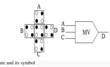
In QCA the most important logic gate is the majority gate. Fig.4 represents a majority gate with 3- inputs and
1-output. In this arrangement, the electrical field effect of each input on the output is identical and additive, due to
this any input ("logic 0" or "logic 1") that is in majority in the gate then becomes the state of the output cell —
hence the gate's name [12]. If inputs A and B are set to logic ―0‖ and input C is set to logic ―1‖, then the output lies in logic ―0‖.
Fig.4 QCA Majority Gate and its symbol
1.2.1.1 AND - OR Gate
Majority Gate can act as both AND (or) OR gate by fixing the polarization. When one input C is kept constant
as logic ―0‖ then it act as AND gate and if C is logic ―1‖ then it act as OR gate.[6] The majority gate performs a three-input logic function. Consider the inputs is A, B and C, then the logic function of the majority
gate is given as in (1):
M (A, B, C) = A.B + B .C + A.C (1)
By assigning a constant value to the polarization of one input to the QCA majority gate as logic ―1‖ or logic ―0,‖ it can act as an AND or OR gate as per equations (2) and (3):
AND (A, B) = M(A,B,0) = AB (2)
960 | P a g e
1.2.1.2 Inverter
The next significant component of QCA is the inverter. The general idea of inverter is that, the cells that are
aligned in a serial manner acts as a wire and those placed in a parallel manner acts as an inverter. A QCA layout
of an inverter circuits are shown in Fig.7 and Fig.8
Fig.5 3-input Majority Gate designed in QCA
Fig. 6 Logic Functions: (a) AND Gate(b) OR Gate
Fig.7 Standardimplementation of inverter
961 | P a g e
II.CLOCKS IN QCA
There is a connection between Quantum-dot Cells and Cellular Automata. Cells can occupy one of 2 states and
the change of state in a cell is determined by the state of its adjacent neighbors. However, a method to govern
data flow is necessary to determine the direction in which state transition happens in QCA cells [21]. The clocks
of a QCA system is used for the automation and controlling data flow direction. Fig.9 shows the four phases of
clocking in QCA. The QCA clocking is carried out in four phases to regulate the tunnel barriers between the
quantum dots.
In the first clock phase (switch), QCA cells begin unpolarized with inter-dot potential barriers low. During this phase, barriers are increased and the QCA cells become polarized according to the state of their input
cells. It is in this clock phase, that real switching (or computing operation) occurs. At the end of this clock
phase, barriers are increased such that it suppresses any electron tunneling and the cell states are fixed.
During the second clock phase (hold), barriers are maintained high so the outputs of the sub array that has
just switched can be used as inputs to the succeeding stage.
In the third clock phase (release), barriers are reduced and cells go to an unpolarized state.
In the fourth clock phase (relax), cell barriers remain lowered and cells remain in an unpolarized state.
962 | P a g e
III. EXISTING METHOD
The full adder based on three inputs MG is shown in Fig.10. To implement ripple adders in QCA,
three input MG based architecture is used [21].
Fig.10 Full adder schematic
Consider ith bit stage for given n-bit addends, X = xn−1,...,x0 and Y= yn−1,...,y0 then propagate term pi = xi +
yi and generate term gi = xi . yi are obtained. At (i-1)th bit position the first carry is generated. The conventional
CLA logic given in (4) is used to compute carry. The last mentioned can be rewritten as reported in (5) by using
Theorem 1 and 2 explained in [2]. In this way the circuit functions like RCA and only one Majority Gate is
needed to propagate the carry to following bit position. But in conventional circuits, two cascaded MGs are
required to perform the same operation. This QCA adder has worst case path nearly half when compared to
conventional QCA design [3]:
ci+2 = gi+1 + pi+1 · gi + pi+1 · pi · ci (4)
ci+2 = M(M (ai+1, bi+1, gi ) M (ai+1, bi+1,pi )ci ) (5)
To design novel 2-bit module shown in Fig.11,the equation (2) is used and the carry Ci+1 =M ( pigi ci ) is
obtained [21].
963 | P a g e
The cascading of n/2 2 bit modules gives n-bit adder [21].Initially carry-in of the adder is considered as 0 andinitial propagate p0 term is not considered. The carry bits are generated first and sum is generated finally by
taking carries generated as input. Basic Module is designed as shown in Fig.12 (a). From this module, n-bit
adders are developed and simulation results are verified using truth table.
Fig.12 (a) Basic Module of Adder Fig.12 (b) Simulation result
Fig.13 4-bit Ripple Carry adder and simulation results
964 | P a g e
IV. PROPOSED ADDER
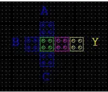
4.1 5-input Majority Gate
The five-input majority gate as shown in Fig.15(a) is the best choice for the full adder, because it is formed by
ordinary cells, the inputs and outputs are not enclosed by the other cells, and they can be computed easily. This
design is suitable to implement larger QCA circuits. In order to minimize the number of majority gates and
inverters, a 5-input majority gate using multilayer is proposed. A five-input majority gate is a logic gate whose
output is 1 only if 3 or more of its inputs is 1.
(a) 5-input Majority Gate
(b) Layout of 5 input Gate
Fig.15 Five-Input Majority Gate
The Boolean function of a five-input majority gate is:
M (A, B, C, D, E) = ABC + ABD + ABE + ACD + ACE + ADE + BCD + BCE + BDE + CDE (6)
A 5-input majority gate can be designed using various concepts. The block diagram of Full adder using
proposed 5-input majority gate is shown in Fig.16. This Majority Gate can act both as an AND gate (or) OR
gate. When any 2 inputs are ‗0‘ it act as an AND gate and when any 2 inputs are ‗1‘ it act as an OR gate. By
using this Majority Gate, a 3-input AND gate and also a 3-input OR gate can be implemented. These functions
are:
M (A,B,C,0,0) = ABC (7)
965 | P a g e
Full adder is designed using Multilayer architecture as shown in Fig.17. Layer 1 has one input E, layer 3 has 3-inputs A, B, C, and layer 5 has one input D. The needed output is obtained from layer 3. In this structure, the
output is not enclosed by the other cells, and therefore, it can easily be accessed. In other words, this structure
does not need any wire crossover to propagate the output signal. Hence, the output can be easily fed into the
input of the other QCA circuits. The use of three layers to implement a 5-input majority gate using multilayer
approach is necessary because the input signals get inverted as signal move across the layers.
Fig.16 Block Diagram of Full adder using 5-input Majority Gate
The layout of 5-input Majority Gate based Full adder is shown in Fig.18. By using this module the 4-bit adder is
designed as shown in Fig.20. It uses one clock zone and there is no delay between input and output.
966 | P a g e
Fig.18 Three different layers of proposed Full adder
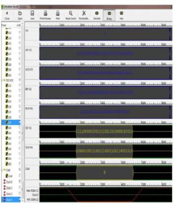
Fig.19 Simulation result of Basic Module
967 | P a g e
Fig.21 Simulation result of 4-bit Ripple Carry adder
Fig.22 64-bit Ripple Carry adder
From the Basic module n-bit adders are designed by increasing the clock phases.Fig.22 and Fig 23 shows the
64-bit adder designed based on the concept of multilayered design by combining the 32-bit adder and increasing
the clock phases for each bit and its simulation results. Its simulation result is checked as per truth table of 64-bit
968 | P a g e
Fig.23 Simulation result of 64-bit Ripple Carryadder
The Carry and Sum is generated and checked for each case. This outstrips all state-of-the art competitors and
reduces area-delay efficiently than previous designs. The adder designed is anticipated to span over a
complexity of 4032 (cell count) and 7.14 μm2 of active area in 321/2 clock phases.
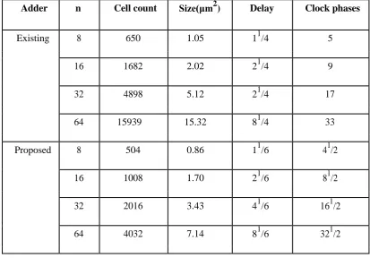
V. PERFORMANCE ANALYSIS
Table 1 shows the comparison result of proposed method with existing method for operands ranging from
8-64 bits. From this it is analyzed that the cell count of proposed method is significantly reduced when
compared to existing method and it achieves the lowest area and delay. Therefore the proposed design
969 | P a g e
Table 1 Result Comparison
Adder
n
Cell count
Size(μm
2)
Delay
Clock phases
Existing
8
650
1.05
1
1/4
5
16
1682
2.02
2
1/4
9
32
4898
5.12
2
1/4
17
64
15939
15.32
8
1/4
33
Proposed
8
504
0.86
1
1/6
4
1/2
16
1008
1.70
2
1/6
8
1/2
32
2016
3.43
4
1/6
16
1/2
64
4032
7.14
8
1/6
32
1/2
VI. CONCLUSION AND FUTURE WORK
The optimized design of Ripple Carry adder is proposed. The proposed Adder is simulated using QCA designer
tool 2.0.2 Version and is efficient in terms of cell count and area. The proposed work has shown that it is
possible to significantly reduce the number of cells required to design basic components, such as adder circuits,
by utilizing the Majority Gate with more number of inputs. In addition to this, the proposed adder is designed
using Multilayer concept which reduces the area significantly than existing methods. The Proposed adder
(64-bit) spans over a complexity of 4032 (cell count) covering 7.14 μm2 of active area and shows a delay of only
81/6 clock cycles, that is just 321/2 clock phases. An interesting extension of the proposed work could be the
automation of the optimizations in order to make it possible to synthesize more complex circuits. The cell count
can further be reduced by using 7, 9 input Majority Gates.
REFERENCES
[1] AmmarSafavi.A and Mohammad Mosleh.B (2013),An Overview of Full Adders in QCA Technology‖,
International Journal IJCSNS, vol. 1, no. 4, pp. 2345-3397.
[2] ArmanRoohi, HosseinKhademolhosseini, Samira Sayedsalehi and KeivanNavi (2014), A Symmetric
Quantum-dot Cellular Automata design for 5-input Majority Gate‖,Springer Science (J Comput Electron),
970 | P a g e
[3] BhupeshBishnoi , Giridhar, M,Dr.BahnimanGhosh and Nagaraju.M (2012), Ripple Carry Adder using FiveInput Majority Gates‖, IEEE Trans. , vol. 12, no. 6, pp.978-1-4673-5696.
[4] FirdousAhmad,GhulamMohiuddinBhat and Peer ZahoorAhmaad (2014), Novel Adder Circuits Based on
Quantum-dot Cellular Automata (QCA)‖, Scientific research, vol. 5, pp. 142-152.
[5] Gregory L.Snider et al., (1999), Quantum-dot Cellular Automata: Line and Majority Logic Gate‖,
Japanese Journal of Applied Physics, vol. 38, pp.7227-7229.
[6] Heumpil Cho and Earl E. Swartzlander (2007), Adder design and analysis for Quantum-dot Cellular
Automata‖, IEEE Transactions on Nano technology, vol.6, no.3, pp.1536–125X.
[7] KeivanNavi, Samira Sayedsalehi, RaziehFarazkish and MostafaRahimiAzghadi (2010), Five-Input
Majority Gate, a New Device for Quantum-dot Cellular Automata‖, Journal of Computational and
theoretical Nanoscience., vol. 7, no. 8, pp.1546-1955.
[8] Lent.C.S ,Tougaw.P.D and Porod.W (1994) , Quantum Cellular Automata: The Physics of
Computing with Arrays of Quantum Dot Molecules‖, PhysComp: proceedings of the Workshop on Physics
and Computing, IEEE Computer Society Press, pp.5-13.
[9] Liang Lu ,Weiqiang Liu, Maire O‘Neill and Earl E.Swartzlander (2013), QCA Systolic Array Design‖,
Proc. IEEE, vol. 62, no. 3, pp. 0018-9340.
[10]Orlov.O.A et al., (1997),Realization of a Functional Cell for Quantum-Dot Cellular Automata‖,
Science, vol. 277, no. 5328, pp. 928-930.
[11]Perri.S and Corsonello.P (Nov 2012), New methodology for the design of efficient binary addition in
QCA‖, IEEE Trans. Nanotechnology, vol. 11, no. 6, pp.1192–1200.
[12]QCA Designer Website: http://www.mina.ubc.ca/qcadesigner
[13]Rui Zhang et al., (2007), Majority and minority network synthesis with application to qca-, set-, and
tpl-based nanotechnologies‖, IEEE Trans. on CAD of Integrated Circuits and Systems, pp.1233–1245.
[14]Samir Roy et al., (2006), Minority gate oriented logic design with quantum-dot cellular automata‖, In
ACRI, pp.646–656.
[15]Shah.N.A, Khanday.F.A and Bangi.Z.A (2012), Quantum-dot Cellular Automata based Efficient BCD
Adder structure‖, International Journal CISME, vol. 2, no. 2, pp. 11-44.
[16]Sivaraj.P and KavinPrakash.C (2014), Speed Efficient Adder using Quantum-dot Cellular Automata‖,
International Journal IJARCST, vol. 2, pp. 2437-9817.
[17]StefaniaPerri and Pasquale Corsonello (2012), New methodology for the design of Efficient Binary
Addition circuits in QCA‖, Proc. IEEE, vol. 11, no. 6, pp. 1536-125X.
[18]Timler.J and Lent.C.S (2002), Power Gain and Dissipation in Quantum dot Cellular Automata‖, Journal of
Applied Physics, vol. 91, no. 2, pp. 823-831.
[19]Tina Suratkar (2013), Five-Input Complex Gate using Quantum-dot Cellular Automata‖, International
Journal of Advanced Research in Electrical ,Electronics and Instrumentation Engineering., vol. 2, Issue 4,
pp.2278-8875.
[20]Tougaw.P.D andLent.C.S (1994), Logical Devices Implemented Using Quantum Cellular Automata‖,
971 | P a g e
[21]Vankamamidi.K et al., (2005), Tile-based design of a serial memory in QCA‖, In GLSVSLI ‘05, NewYork, NY, USA, ACM, pp. 201–206.
[22]VikramkumarPudi and Sridharan.K (2011), Efficient Design of Hybrid Adder in Quantum-dot Cellular
Automata‖, Proc. IEEE, vol. 19, no. 9, pp. 1063-8210.
[23]Walus.K and Jullien.G.A (2006), Design tools for an emerging SoC technology: Quantum-dot cellular