OPTIMIZATION AN ANECHOIC CHAMBER WITH RAY-TRACING AND GENETIC ALGORITHMS
S. M. J. Razavi and M. Khalaj-Amirhosseini
College of Electrical Engineering
Iran University of Science and Technology Tehran, Iran
Abstract—Anechoic chambers are used for both emission and immunity testing but the ferrite tiles used to line the inside of the chamber are extremely expensive.This paper describes a method of reducing the number of tiles, whilst ensuring a reliable test environment.
In this paper, the ray-tracing method for waves propagation is used for evaluation of the reflectivity level of an anechoic chamber, and genetic algorithms are used.And use genetic algorithms to optimize the layout of ferrite tile absorber in a partially lined enclosure to produce a best performance.
The results show that it is possible to cover just 80% of the surface of the enclosure with ferrite absorber and obtain good agreement by fully lined enclosure with an error of less than 3 percent over the whole test points.
1. INTRODUCTION
The need for indoor testing of electromagnetic radiating devices, which began in the early 1950s [1], has led to a number of companies providing chambers and absorber products supporting a range of electromagnetic testing requirements.Microwave anechoic chambers are currently in use for a variety of indoor antenna measurements, electromagnetic interface (EMI) measurements, and electromagnetic compatibility (EMC) measurements [2].The mentioned chambers provide sufficient volume for an antenna to generate a known field. This volume is called “quiet zone” and the level of reflected waves within it determines the performance of the anechoic chamber.
optimized for this application.The most common material is ferrite tile.The ferrite tiles are expensive and the room strength required to support the weight of the tiles (of the order of 30 kg/m) adds to the cost.
The need for decreasing the cost, led to develop some new optimized analytical and practical methods.Based On the experiments [3], with 80% of Fresnel zone absorbing coverage, the variation of theE-field is very uniform at all frequencies above 300 MHz and the maximum error is 1.4 dB. Some optimized methods by using additional absorbers and shifted absorbers and new absorber lining of optimized material are proposed in [4].
The method offered in this paper describes a new technique to reduce the need for full coverage of lining material and optimize the layout of absorbing material tiles to reach a good performance for the chamber and minimize the cost.The offered method has been simulated via computer programs and validated with CST MICROWAVE STUDIO.
The modeling technique is described in Section 2.Section 3 presents the results of this work.Conclusions are given in Section 4.
2. MODELING TECHNIQUE
In first step the reflectivity level of an anechoic chamber is evaluated for dipole antenna using the ray-tracing method.The method is described in subsection 2.1. The next step is explained the genetic algorithm to optimize the layout of ferrite tile absorber in a partially lined enclosure to produce best performance.The algorithm is described in subsection 2.2. The model of ferrite tile in the wide frequency range is described in subsection 2.3.
2.1. Ray-Tracing Method
along the φ.Coordinate.Besides, for the dipole antenna, the axis of the dipole is chosen to be the localY axis of the spherical coordinates so that the field strengths of the initial tubes are symmetry inφ and the tubes along the localY axis can be neglected.Only the significant radiation regions need to be covered by those ray tubes, which are then traced one by one to find their GO contributions at the location of the receiving antenna.
The ray tracing technique provides a relatively simple solution for indoor wave propagation [6–9].However, it should be noted that the application of GO is incorrect when the object of interest has the dimensions that are comparable or less than wavelength.
s s
) , , (
0 abc
P
) , ,
( 2 2 2
2 x y z
P
) , , ( 1 1 1
1 x y z
P n(n1,n2,n3)
^
^
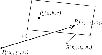
Figure 1. A ray propagates from P1 toP2 on an intercepting plane.
The basic ray-tracing procedure is described below.
1) Each ray of the ray tubes is traced to find an incident point (as shown in Fig.1) where a ray propagates from a point P1(x1, y1,
z1) to an incident pointP2(x2,y2,z2) on an intercepting interface.
The coordinates of the incident pointP2 can be determined from
the following expression:
(x2, y2, z2) = (x1, y1, z1) +ssˆ (1)
where ˆs is the directional vector of the incident ray ands is the path length of the ray.For a flat interface defined with a normal unit vector ˆn = (n1, n2, n3) and a point P0 = (a, b, c) on the
interface, the path length is given by
s= nˆ·(P0−P1) ˆ
n·ˆs (2)
This is obtained from the relation −−−→P0P2 ·nˆ = 0.For a
length fromPi is the true intercepting point.Except for the initial
rays from the transmitting antenna, point P1 is on an interface,
too.Thus, for each interface that may start the ray tracing, based on the relative geometry of the structures, a list of the searching order over the other interfaces to find the incident point may be generated before starting the ray-tracing procedure to improve program efficiency.
2) When a ray tube incidents on an interface, a reflected and a transmitted ray tube is generated according to Snell’s law and the local plane wave approximation.The reflection and transmission coefficients derived for a plane wave illuminating a flat interface of two materials are employed [7].
3) A ray tube will be terminated if:
1) It exits outdoor or leaves the simulated domain;
2) It hits any edge of the structures (i.e., diffractions are neglected);
3) The magnitude of the E-field is less than a threshold.For 3), the total length of the ray paths from the transmitting antenna to the present location is used to approximate the spreading factor of the E-field.A Convergence test should be performed to set the proper threshold, which is defined as the percentage of the reference field strength at 1 m from the transmitting antenna.If both the reflected and transmitted rays are significant, one of the ray tubes is stored by pushing it into a “stack,” while the other one is continuously traced. The data set for each stored ray tube includes the directional vectors, positions, total path lengths, and E-field phasors (excluding the spreading factor) of the four rays.If both ray tubes are ended, a previously saved ray-tube data set is then popped from the stack and the ray-tracing procedure is started again.When the stack is empty, a new initial ray tube from the transmitting antenna is traced until finished. Multiple reflections and transmissions through walls, ceiling, stairs, floors, and other electrically large bodies can be simulated both in air and in the structures to properly model wave propagation and penetration in buildings.
R
O Tube Ray
Wall
3 P
4 P
Figure 2. A ray tube passing a receiving antenna at R.
a) Find the four intercepting pointsOi’s of the ray-tube incident
on a plane that is perpendicular to one of the four rays and contains the receiving point.
b) Determine the four angles αi’s formed Oi’s and R with
0≤αi≤π.
c) If the sum of the four angles αi’s is less than 2π, then the
ray tube does not pass through R.However, 1.999π was actually employed instead of 2πin the comparison and double precisions were used to avoid possible numerical mistakes in determining the interception.The E-field vector phasors of the tubes passing the receiving point are superposed to obtain the E-field at this field point [5].All the field points in the receiving room may be checked and evaluated during 4) to obtain the field distributions more efficiently.
5) From the geometrical optics, the E-field of the ray tube at the receiving point can be determined from the following equation:
E =E0·
Ri
·Ti
·e−rili
·SF (3)
where −→E0 is the E-field at a reference point r0, Ri
and
Ti
are, respectively, the reflection and transmission coefficient
dyads along the whole ray path, e−rili
contribution starting from r0, and SF is the spreading factor.
From the conservation of energy flux in a ray tube [7], SF can be obtained by using
SF =A0
√
A (4)
whereA0 and A are the cross-sectional areas of the ray tubes at
the reference pointr0 and the field pointr, respectively.The sum
of the areas of the four triangles on the intercepting quadrilateral at the receiving point as shown in Fig.2 may be evaluated to approximate the cross-sectional areaA.
In this paper transmission ray tubes are attenuated and only reflection ray tubes are traced at each interface.The spreading factor is determined from the cross-sectional area of the ray tube; this ray-tube tracing method can be applied to find the reflection contribution for rather complicated structures.
2.2. Genetic Algorithm
Ferrite tiles are generally 10 cm squares.The size of anechoic chamber means that the number of 10-cm-square positions that may be occupied by a tile is of the order of 10000 (for a 9 m×9 m×10 m room).The room under investigation here (cover just 80% of its surface) would need approximately 417600 tiles.To search manually for the best performance in a problem of this size would be impossible.An automated system is necessary and the use of genetic algorithms is suited for this type of search.
Both possible solutions are then replaced in the population and two more solutions are selected at random (note that this may select one possible solution more than once and in fact may select good solutions many times) and one is chosen to be another parent in the same way. Tournament selection was used as it has been found to provide a faster convergence than other selection methods for a range of problems [9]. The Cost Factor was monitored during the runs and was found to tend toward the final result without any significant deviations, which implies that the algorithms used were convergent for this particular problem.
Once the parents have been selected, two parents are then “crossed over” to produce two children.In this a random section of the binary string from one parent is removed and replaced with the same part of the string from the second parent (and vice versa) to generate two “children” for the next generation.As the string in this case represented positions on the walls of the enclosure, the portions of the string which were swapped were not contiguous but were chosen to represent rectangular blocks of tiles.
To enable the work to be carried out within the time available, the problem space was reduced by dividing the surface area of the enclosure into 0.25-m squares, each one of which was either fully tiled or not tiled. The position of each square was then assigned to a point on the binary string with the 1/0 s indicating tiles/no tiles.The numbers of cells for this case (9 m×9 m×10 m room) are 2090 and equal by the size of string.This significantly reduced the number of possible permutations available and also simplified the problem when the tiles were installed in the enclosure.
2.3. Representing Ferrite Tiles
Ferrite tile absorbers are made of solid ferrite about 6 mm thick or in a grid construction approximately 20 mm thick.These ferrite tiles cannot be represented accurately over a wide frequency range.This is due to the change in their permeability with frequency.They can be represented using the method of [18–23] but the fine mesh required precludes room modeling due to the very large amount of computer memory required.
These problems have been partially overcome by the development, at York, of a frequency-dependent boundary which accurately models both the phase and amplitude of the reflection coefficient of solid ferrite tiles.This technique can be used with any mesh size to model the action of ferrite absorbing tiles.
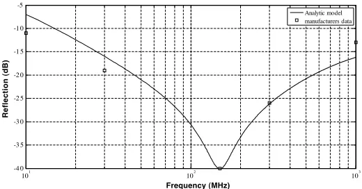
the second-order function as
F(s) =−
s2+ 2aωns+ω2n
k(s+d)(s+e) (5) where s is the Laplace variable.The reflection has a minimum magnitude ρmin when s = jωn.The coefficients of the function can
be determined from a few points on the reflectivity curve (magnitude only).The equation includes the pole at s = −e to limit the value of reflection coefficient at high frequencies.Without this pole, the reflection coefficient could become greater than 1 at higher frequencies.
For larges
F(s)≈ −
1
k
(6)
And asstends to zero
F(s)≈ −
ω2n
kde (7)
We know that the reflection coefficient for the tile tends to−1 at low frequencies so we can match the functions by taking key points on the reflectivity curve of the ferrite tile.Therefore,
ωn= 2πfmin (8)
wherefminis the frequency of the reflection minimumρmin.The factor
kis given by
k= 1
ρh
(9)
where ρh is the magnitude of the reflection coefficient at the highest
frequency part of the curve (where the reflection coefficient levels out) The pole eis then determined by
e= 2πfu
ρu
(10)
wherefuis the frequency of a point well above the reflection minimum,
before the reflection coefficient levels out, and ρu is the magnitude of
the reflection coefficient at that point.
The Damping factor a can be expressed as a function of earlier factors and the minimum value of the reflectivityρmin
a= keρmin 2ωn
101 102 103 -4 0
-3 5 -3 0 -2 5 -2 0 -1 5 -1 0 -5
Frequency (MHz)
Reflection (dB)
Analytic model manufacturers data
Figure 3. Modeled reflectivity curve for Philips tiles.
The pole position,d, is fixed by the fact that the reflectivity [and henceF(s)] must become−1 asstends to zero so that rearranging (7) we obtain
d= ω
2 n
ke (12)
2.4. Settings for Optimization
Since the final aim of the work was to optimize the tile configuration with an automated computer program, a single figure of merit was required to represent the quality of each tile configuration.
The figure of merit chosen for this work was generated from the difference between the reflectivity level (RL) in the completely lined absorber anechoic chamber (RLCAC) and the RL in the partially lined absorber anechoic chamber (RLPAC).The reflectivity level, RL, of an anechoic chamber is defined as
RL =
ERi
EF s
(13)
where ERi is the reflected field, at receiving point R, due to the ith
Reflected ray andEF s is the free space field at point, R.the figure of
merit is obtained by Equation (14).
Cost=
f requency
testpoints
(RLCAC – RLPAC)2 (14)
3. RESULTS
The anechoic chamber dimensions used were 9 m×9 m×10 m.The positioning of the excitation and test points in the enclosure was chosen to comply with the requirements of the draft concept standard: EN 50147-3 Emission measurements in fully anechoic chambers.The position of excitation antenna was (3 m 3 m 4 m).The test points selected for optimization process is shown in Fig.4. These points are numbered from 1 to 15 in result figures.
m 9 m 3 m 10 m 9 TOP MID LOW m 8 . 0 m 8 . 0 1 2 3 4 5 6 7 8 9 10 11 12 13 14 15 m 4 m 3 m 6 . 0 2 3
4 1 5
Position Antenna Excitation s Po Test Volume int m 4 . 2
Figure 4. Positions of excitation antenna and 15 test point’s volume.
The first run was for a dipole antenna at 100 MHz frequency.The optimization process was begun with 1000 generations to reduce the cost factor.The final layout for tiles was obtained after nearly 40 iterations for optimization process.This layout is shown in Fig.5.
To validate this layout, the predicted and simulated (with CST MICROWAVE STUDIO) results were compared in Fig.6. The agreement between predicted and CST simulated result, in partially lined absorber enclosure, is good with an error of less than 5 percent over 15 test points.
x(m)
y(
m)
layer (z=0)
1 2 3 4 5 6 7 8
2 4 6 8
x(m)
y(
m
)
layer (Z=10)
1 2 3 4 5 6 7 8
2 4 6 8
x(m)
z(
m
)
layer (y=0)
1 2 3 4 5 6 7 8
2 4 6 8
x(m)
z(
m
)
layer (y=9)
1 2 3 4 5 6 7 8
2 4 6 8
z(m)
y(
m
)
layer (x=0)
1 2 3 4 5 6 7 8 9
2 4 6 8
z(m)
y(
m
)
layer (x=9)
1 2 3 4 5 6 7 8 9
2 4 6 8
Figure 5. Optimized layout for dipole antenna excitation at 100 MHz (black = no tiles, white = tiles).
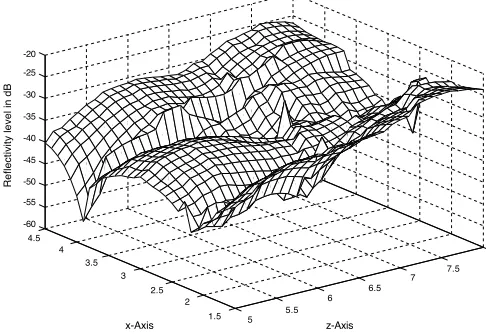
The Figs.7 and 8 show the reflectivity level of the fully and partially lined absorber enclosure.
0 5 10 15 0.03
0.035 0.04 0.045 0.05 0.055
number of point test according to Fig. 4
amplitude of electic field (volt/meter)
fully liened ferrite tile enclosure partially liened ferrite tile enclosure CST MICROWAVE STUDIO results
Figure 6. Compared amplitudes of electric field in the 15 test points (predicted and simulated).
5 5.5
6 6.5
7 7.5
8
1.5 2 2.5 3 3.5 4 4.5 -60 -55 -50 -45 -40 -35 -30 -25 -20
z-Axis x-Axis
Reflectivity level in dB
Figure 7. Reflectivity level of fully lined absorber enclosure at 100 MHz.
5 5.5
6 6.5
7 7.5
8
1.5 2 2.5 3 3.5 4 4.5 -60 -55 -50 -45 -40 -35 -30 -25 -20
z-Axis x-Axis
Reflectivity level in dB
Figure 8. Reflectivity level of partially lined absorber enclosure at 100 MHz.
RL in partially lined absorber enclosure at point 1 RL in fully lined absorber enclosure at point 1
100 150 200 250 300 350 400 450 500 -45
-40 -35 -30 -25 -20 -15
Frequency (MHz)
Reflectivity level in dB
-50
Figure 9. Compared reflectivity level of enclosure in the test point 1 at the wide frequency range.
RL in partially lined absorber enclosure at point 6 RL in fully lined absorber enclosure at point 6
100 150 200 250 300 350 400 450 500 -45
-40 -35 -30 -25 -20 -15
Frequency (MHz)
Reflectivity level in dB
Figure 10. Compared reflectivity level of enclosure in the test point 6 at the wide frequency range.
100 150 200 250 300 350 400 450 500 -45
-40 -35 -30 -25 -20 -15
Frequency (MHz)
Reflectivity level in dB
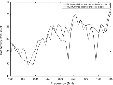
RL in partially lined absorber enclosure at point 11 RL in fully lined absorber enclosure at point 11
Figure 11. Compared reflectivity level of enclosure in the test point 11 at the wide frequency range.
4. CONCLUSION
good optimization, the 20% reduction of the coverage of lining ferrite tile, led to an acceptable 2 dB increase of reflectivity level of anechoic chamber.The final obtained layout has a good performance in the frequency range 100–500 MHz.
REFERENCES
1.Emerson, W.H., “Electromagnetic wave absorbers and anechoic chambers through the years,” IEEE Transactions on Antennas and Propagation, Vol.21, No.4, July 1973.
2.Marquart, N.P., “Experimental anechoic chamber measurements of a target near an interface,” Progress In Electromagnetics Research, PIER 61, 143–158, 2006.
3. Kineros, C.and V.Ungvichian, “A low cost conversion of semi-anechoic chamber to fully semi-anechoic chamber for RF antenna measurements,” USA, 2003.
4.Bornkessel, C.and W.Wiesbeck, “Numerical analysis and optimization of anechoic chambers for EMC testing,”IEEE Trans. Electromagn. Compat., Vol.38, No.3, 499–506, August 1996. 5. Kim, H.and H.Ling, “Electromagnetic scattering from an
inhomogeneous object by ray tracing,” IEEE Trans. Antennas Propagat., Vol.40, 517–525, May 1992.
6. Chung, B.-K., C. H. Teh, and H.-T. Chuah, “Modeling of anechoic chamber using a beam-tracing technique,” Progress In Electromagnetics Research, PIER 49, 23–38, 2004.
7. Jin, K.-S., T.-I. Suh, S.-H. Suk, B.-C. Kim, and H.-T. Kim, “Fast ray tracing using a space-division algorithm for RCS prediction,” Journal of Electromagnetic. Waves and Appl., Vol.20, No.1, 119– 126, 2006.
8. Wang, N., Y. Zhang, and C.-H. Liang, “Creeping ray-tracing algorithm of UTD method based on nurbs models with the source on surface,”Journal of Electromagnetic. Waves and Appl., Vol.20, No.14, 1981–1990, 2006.
9. Liang, C.-H., Z.-L. Liu, and H. Di, “Study on the blockage of electromagnetic rays analytically,” Progress In Electromagnetics Research B, Vol.1, 253–268, 2008.
10.Balanis, C.A., Advanced Engineering Electromagnetics, Wiley, New York, 1989.
12.Meng, Z., “Autonomous genetic algorithm for functional optimization,” Progress In Electromagnetic Research, PIER 72, 253–268, 2007.
13.Tian, Y.-B.and J.Qian, “Ultraconveniently finding multiple solutions of complex transcendental equations based on genetic algorithm,”Journal of Electromagnetic. Waves and Appl., Vol.20, No.4, 475–488, 2006.
14. Mouysset, V., P.A.Mazet, and P.Borderies, “Optimization of broadband top-load antenna using micro-genetic algorithm,” Journal of Electromagnetic. Waves and Appl., Vol.20, No.6, 803– 817, 2006.
15. Chen, X., D.Liang, and K.Huang, “Microwave imaging 3-D buried objects using parallel genetic algorithm combined with FDTD technique,” Journal of Electromagnetic Waves and Appl., Vol.20, No.13, 1761–1774, 2006.
16. Ngo Nyobe, E.and E.Pemha, “Shape optimization using genetic algorithms and laser beam propagation for the determination of the diffusion coefficient in a hot turbulent jet of air,” Progress In Electromagnetics Research B, Vol.4, 211–221, 2008.
17. Su, D., D.-M. Fu, and D. Yu, “Genetic algorithms and method of moments for the design of PIFAS,”Progress In Electromagnetics Research Letters, Vol.1, 9–18, 2008.
18.Dawson, J.F., “Improved magnetic loss for TLM,”Electron. Lett., Vol.29, No.5, 467–468, 1993.
19. Chung, B.-K. and H.-T. Chuah, “Modeling of RF absorber for application in the design of anechoic chamber,” Progress In Electromagnetics Research, PIER 43, 273–285, 2003.
20.Dawson, J.F., “Representing ferrite absorbing tiles as frequency dependent boundaries in TLM,” Electron. Lett., Vol.29, No.9, 791–792, 1993.
21. Chamaani, S., S.A.Mirta, M.Teshnehlab, M.A.Shooredeli, and V.Seydi, “Modified multi-objective particle swarm optimization for electromagnetic absorber design,” Progress In Electromagnet-ics Research, PIER 79, 353–366, 2008.
22. Khajehpour, A.and S.A.Mirtaheri, “Analysis of pyramid EM wave absorber by FDTD method and comparing with capacitance and homogenization methods,” Progress In Electromagnetics Research Letters, Vol.4, 123–131, 2008.