A Novel Miniaturized Frequency Selective Surface
with Very Stable Performance
Huangyan Li*, Qunsheng Cao, and Yi Wang
Abstract—A miniaturized frequency selective surface (MFSS) that has very stable performance is designed based on the stepped-impedance element (SIE) structure. Significant couplings can be introduced by overlapping one metallic layer above the SIE structure. The large overlapping areas between the two metallic layers is beneficial to further miniaturizing the element size. Therefore, the physical size of the MFSS unit cell can be reduced to 0.054λ×0.054λ. In addition, the MFSS is proved to have excellent stability towards incident angles (up to 75◦) and polarizations. A careful equivalent circuit model is presented to explain the physical principle of the proposed design. Finally, a prototype is fabricated and tested, and the simulation results are in agreement with the experimental observations.
1. INTRODUCTION
Frequency selective surface (FSS) usually consists of an array of metallic patches or apertures that are arranged periodically [1]. FSSs work as a kind of spatial filter, which controls the transmission and reflection properties of electromagnetic waves. FSSs have been widely applied in many fields such as absorbers [2, 3], antenna radomes [4, 5] and electromagnetic compatibility [6].
The miniaturization technique is highly desired to help FSSs achieve better performance in aspects of frequency, incident angle and polarization. It benefits a finite FSS in placing enough elements in a limited area, allowing it to perform as an infinite FSS array. In many practical applications such as curved antenna radomes [7], miniaturized FSSs can be employed to achieve stable transmission performance and avoid the early onset of grating lobes.
To realize the objective of miniaturization, many different methods have been put forward [8–11]. The meandering technique is commonly employed in miniaturizing FSSs by increasing the resonant length of the structure [8, 9]. However, there are limitations to increase the resonant length within a certain area, and it also increases the difficulty in fabrication as the spacing between components becomes smaller. Loading lumped elements, such as lumped inductors and lumped capacitors, is also an useful approach for miniaturization [10], but the lumped components will increase the fabrication cost and are vulnerable to environmental impacts. One possible and easy way to decrease the size of the FSS is proposed in [11], where significant distributed capacitance is introduced by coupling another metallic layer on the other side of the substrate. In addition, FSS designs often suffer from stability issues like the sensitivity to incident angles and polarizations. An SIE structure with a simple pattern is presented in [12], which demonstrates good angle stability.
For this paper, a miniaturized frequency selective surface (MFSS) with excellent stability towards incident angles and polarizations is presented. The metallic SIE structures are set on one side of the dielectric layer, with an additional metalized patch array on the other side. The advantage of the proposed structure lies in its higher miniaturization level, better stability and lower cost. The
Received 16 May 2017, Accepted 17 June 2017, Scheduled 5 July 2017 * Corresponding author: Huangyan Li (huangyan [email protected]).
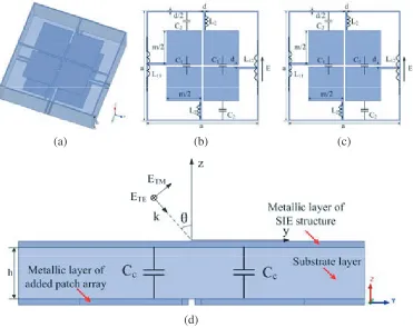
Fig. 1(b), is used here as a basic structure due to its stable performance. Another metallic patch array in Fig. 1(c) is placed above the SIE structure for miniaturization. The cross-sectional view of the MFSS is presented in Fig. 1(d).
(a) (b) (c)
(d)
Figure 1. MFSS configuration. (a) Sketch diagram. (b) Metallic SIE structure. (c) Additional metallic patch array. (d) Side view.
In order to analyze the transmission properties and give more insight into the working mechanism of the MFSS, an equivalent circuit model can be constructed. The equivalent circuit model under a normal electromagnetic wave, with the electric field polarized alongXaxis, is shown in Fig. 2. As shown in Fig. 1(b), the metallic SIE structure can be equivalent to two series resonant circuits consisting of
C1,C2 andL2 in parallel withL1 (L1 =L11+L12), whereC1 is the equivalent gap capacitance between the two metallic square patches, C2 the gap capacitance that comes from the couplings between the square metal patch and the horizontal edge of the metallic square loop, and the equivalent inductance
Figure 2. Equivalent circuit of the MFSS.
this way, two seriesLC resonant circuits can be formed and added symmetrically into the SIE model as the parallel branches. The overlapped metallic region between two metallic layers generates additional coupling capacitance Cc shown in Fig. 1(d), which increases the whole equivalent capacitance. In addition, there are coupling capacitances between the metallic patches that are not directly opposite in the top and bottom layers. To take the mutual couplings into account, four sets (12 in total) of coupling capacitances (i.e., C16, C17, C18;C25,C27, C28; C35,C36,C38;C45, C46, C47) are introduced into the circuit but are not shown in Fig. 2 for clarity. The coupling capacitances have the relation of
C16 = C17 = C25 = C28 = C35 = C38 = C46 = C47 = Cx and C18 = C27 = C36 = C45 = Cy. The subscripts from 1 to 8 indicate the connecting positions of these coupling capacitances, which are also denoted in Fig. 2 correspondingly. The dielectric layer is modeled by a combination of series inductance
LT L and shunt capacitance CT L, which can be calculated by:
LT L = μ0μrh (1)
CT L = ε0εrh/2 (2)
where εo and μo are the relative permittivity and permeability of the air; εr and μr are the relative permittivity and permeability of the substrate, respectively; h represents the substrate thickness.
The equivalent inductance and capacitance of metallic parallel structures can be decided approximately by the following equations [13]:
L = μ0(p/2π) log [csc(πw/2p)] (3)
C = ε0εr(2l/π) log [csc(πs/2l)] (4) where the equivalent inductance is associated with the length p and width w of the metallic parallel structure, and the equivalent capacitance is decided by the side length l and gap widths, respectively.
The coupling capacitance Cc caused by direct face couplings can be calculated by:
Cc=ε0εrS
h (5)
whereS is the overlapped metallic areas.
Detailed parametric analyses of the equivalent circuit can be conducted to readily predict the behavior of the FSS with fair level of accuracy. After that, the initial geometric parameters are optimized in HFSS to improve the bandpass characteristics of the MFSS. Finally, a circuit-level analysis can be conducted in ADS to attain the transmission coefficients of the MFSS. The optimized geometric parameters can be mapped to the initial values for the circuit parameters using Equations (1)–(5), which are then fine tuned using the optimization algorithm in ADS to get the best fit between the circuit response and the HFSS response considering the mutual couplingsCx and Cy.
3. MFSS DESIGN AND NUMERICAL RESULTS
L11 (nH) L12(nH) C1 (pF) C2 (pF) L2 (nH) Cc (pF)
4.569 4.569 0.130 0.013 0.343 0.146
Cadd (pF) Ladd (nH) LT L (nH) CT L (pF) Cx (pF) Cy (pF)
0.231 0.343 1.005 0.016 0.06 0.02
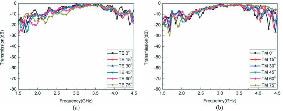
The simulated results of the MFSS are shown in Fig. 3. The operating frequency is 3 GHz with a 25.3% fractional bandwidth for the TE polarization and 26.1% fractional bandwidth for the TM polarization under normal incidence. Besides, it is also shown that the structure is not sensitive to incidence angles (up to 75◦) and polarization modes. In addition, the unit size of the MFSS is miniaturized to 0.054λ×0.054λ, whereλ is the operating wavelength in free space.
(a) (b)
Figure 3. Simulated results of the MFSS. (a) TE mode. (b) TM mode.
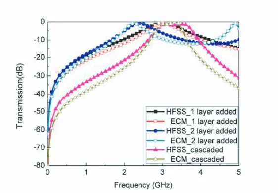
The dimension of the MFSS can be further reduced by adding more coupling layers, which increases the coupling capacitance. One more layer of metallic patch array is considered to be added here. The sketch diagram of the structure with two added layers is illustrated in Fig. 4, and its equivalent circuit model is established in Fig. 5.
In Fig. 6, the transmission properties of the MFSS with two added layers are simulated and compared with that of the MFSS with one added metallic layer. It can be observed that the operating frequency can be decreased from 3 GHz to 2.39 GHz with a 23.3% fractional bandwidth under normal incidence. Therefore, the structure size can be reduced to 0.043λ×0.043λ. The simulation results from HFSS are also verified by the ECM, and they agree well with each other.
Figure 4. Sketch diagram of the MFSS with two added layers.
Figure 5. Equivalent circuit of the MFSS with two added layers.
Structure proposed (2 layer added) 4.4 75 (s) 0.043λ×0.043λ
angle larger than 60◦. Besides, the dimension of the MFSS in this paper is only half the size of the structure proposed in [12] when two layers are added.
Furthermore, high-order characteristics of the stable MFSS can be studied based on the cascading technique. To achieve a second-order performance, two single-layer MFSSs in Fig. 1(a) are cascaded with an air space of 9.5 mm. The transmission curves of the cascaded MFSS are also depicted in Fig. 6, and a sharper transmission response can be observed compared to that of the single-layer MFSS.
(a) (b)
Figure 7. Prototype of the MFSS. (a) SIE structure. (b) Added patch array.
(a) (b)
4. EXPERIMENTAL RESULTS
In order to verify the simulated results, a prototype of the MFSS is fabricated. The MFSS prototype shown in Fig. 7 has 56×56 elements and an overall dimension of 302.4×302.4 mm2. The MFSS is measured in the anechoic chamber for validation, using two antennas and an Agilent N5230C VNA. Two steps are conducted to ensure the accuracy of the measurement: the transmittance are obtained without the MFSS at first; the transmission properties with the MFSS are then attained.
The experimental values of the proposed structure are shown in Fig. 8, and the measured fractional bandwidths for the TE and TM polarizations under normal incidence are 26.1% and 25.6%, respectively. The observational results are in consistent with the simulated results under oblique incidence except that there are some ripples, which might be attributed to the edge diffraction effects of the finite-size prototype.
In addition, as can be observed in Table 4, the fractional bandwidths (FBWs) of TE mode reduce and those of TM mode improve as the incident angles increase from 0◦ to 75◦. The variation tendency of the simulated and measured results is quite consistent with each other although some differences exist, especially for large incident angle such as 75◦. This deviation might result from the limited size of the MFSS prototype since part of incident waves would impinge on the absorber frame around the MFSS under large incident angles.
Table 4. Fractional Bandwidths (FBW) of the MFSS.
Polarization FBW-TE (%) FBW-TM (%)
Angle Simulated Measured Simulated Measured
0◦ 25.3 36.2 26.1 25.6
15◦ 25.4 23.2 28.2 28.4
30◦ 23.0 22.3 30.3 30.7
45◦ 18.7 20.6 37.3 31.2
60◦ 10.2 19.8 40.6 35.2
75◦ 6.7 12.3 84.7 45.1
5. CONCLUSION
An MFSS with very stable performance is proposed in this paper. The single-layer structure possesses a high miniaturization level of 0.054λ×0.054λ, and it can be further miniaturized to 0.043λ×0.043λ
as one more layer is added. The MFSS demonstrates superior stabilization towards incident angles (up to 75◦) and polarizations. The MFSS with stable performance has a promising future in many electromagnetic fields such as radomes, electromagnetic compatibility and so on.
ACKNOWLEDGMENT
The work was funded by the National Natural Science Foundation of China under grant No. 61401199 and and Natural Science Foundation of Jiangsu Province under grant No. BK20140810.
REFERENCES
1. Munk, B. A., Frequency Selective Surfaces: Theory and Design, John Wiley & Sons, 2005.
2. Liu, T., X. Cao, J. Gao, and Q. Zheng, “RCS reduction of waveguide slot antenna with metamaterial absorber,” IEEE Trans. Antennas Propag., Vol. 61, No. 3, 1479–1484, 2013.
surfaces with wide bandwidths,”Electron. Lett., Vol. 42, No. 14, 788–790, 2006.
8. Li, H. and Q. Cao, “Design and analysis of a controllable miniaturized triband frequency selective surface,” Progress In Electromagnetics Research Letters, Vol. 52, 105–112, 2015.
9. Sanz-Izquierdo, B., E. A. Parker, J. B. Robertson, et al., “Singly and dual polarized convoluted frequency selective structures,”IEEE Trans. Antennas Propag., Vol. 58, No. 3, 690–696, 2010. 10. Liu, H. L., K. L. Ford, and R. J. Langley, “Miniaturised bandpass frequency selective surface with
lumped components,”Electron. Lett., Vol. 44, No. 18, 1054–1055, 2008.
11. Deng, F., X. Yi, and W. Wu, “Design and performance of a double-layer miniaturized-element frequency selective surface,” IEEE Antennas Wireless Propag. Lett., Vol. 12, 721–724, 2013. 12. Hussein, M., J. Zhou, Y. Huang, and A. P. Sohrab, “Frequency selective surface with simple
configuration stepped-impedance elements,” Proc. Eur. Conf. Antennas Propag., Davos, CH, Apr. 10–15, 2016.