Dual Input DC-DC Boost Converter with High
Gain and Two Boost Stages for Microgrid
Applications
Diana Xavier1, Rosemin Parackal2
PG Student [PEPS], Dept. of EEE, FISAT, Angamaly, Kerala, India 1
Assistant Professor, Dept. of EEE, FISAT, Angamaly, Kerala, India 2
ABSTRACT:This paper presents high-voltage-gain dc–dc power electronic converter with two boost stages. The suggested topology can be used as multiport converters and draw continuous current from two input sources. They can also draw continuous current from a single source in an interleaved manner. This versatility makes them appealing in renewable applications such as solar farms. The proposed converters can easily achieve a gain of 20 while benefiting from a continuous input current. Such a converter can individually link a PV panel to a dc bus. The validity of the proposed converter are verified by MATLAB\SIMULINK..
KEYWORDS: Diode-capacitor voltage multiplier stages, high voltage-gain dc-dc power electronic converters..
I.INTRODUCTION
The increasing of world energy,air pollution global warming and extension of fosil fuels have made it necessary to look towards renewable sources as a future energy solution.Various renewable sources such as solar energy, wind energy,geothermal energy etc are harnessed for electric energy. The output voltage from most renewable energy sources like photovoltaic, fuel cells or energy storage devices such as super capacitors and batteries deliver output voltage at very low ranges which are not useful for commercial usage. In order to make them to use we have to step up these levels to grid voltage level.With the increased penetration of renewable energy sources and energy storage, high-voltage-gain dc–dc power electronic converters find increased applications in green energy systems. They can be used to interface low voltage sources like fuel cells, photovoltaic (PV) panels, batteries, etc.to the bus in a dc microgrid system . They also find applications in different types of electronic equipment such as high-intensity-discharge lamps for automobile head lamps, servo-motor drives, X-ray power generators, computer periphery power supplies, and uninterruptible power supplies. Typically frequency transformers or coupled inductors are used to achieve high-voltage conversion ratios .The transformer design is complicated and the leakage inductances increase for achieving larger gains, as it requires higher number of winding turns. Consequently, it makes the design more complicated. To achieve high-voltage conversion ratios, a new family of high-voltage-gain dc–dc power electronic converters has been introduced.
II.PROPOSED TOPOLOGY
Fig 1:Proposed topology
In this topology ,one of the input is taken as solar energy and other as battery in case of high gain converter.The output of the high gain converter is then supplied to single phase inverter. The proposed converter can be used to draw power from two independent dc sources as a multiport converter ,or one source in an interleaved manner. They draw continuous input current from both the input sources with low current ripplewhich is required inmany applications, e.g., solar. Several diode-capacitor stages are cascaded together to boost up the voltage which limits the voltage stresses on the switches, diodes, and capacitors.
1.HIGH GAIN DC-DC BOOST CONVERTER AND ITS MODES OF OPERATION
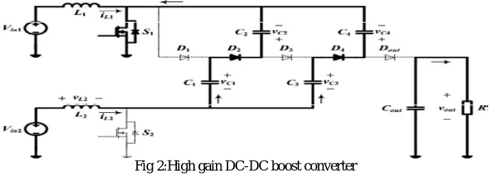
High gain DC-DC boost converter is inspired from a Dickson charge pump.Diode capacitor voltage multiplier stages are integrated with two boost stages at the input. Voltage multiplier stages are used to help the boost stages to achieve a higher voltage gain .conversion ratio depends on duty cycle and number of voltage multiplier stages. For normal operation of the proposed converter, there should be some overlapping time when both the switches are ON and also one of the switches should be ON at any given time .Therefore, the converter has three modes of operation. The proposed converter can operate when the switch duty ratios are small and there is no overlap time between the conduction of the switches.
Fig 2:High gain DC-DC boost converter
The switching frequency of the switches is 100KHz and there are two boost modes which increases the gain of the converter
Fig 3:Switching pulses
MODES OF OPERATION
Mode1
In this mode, both switches S1 and S2 are ON. Both the inductors are charged from their input sources Vin1 and Vin2 . The current in both the inductors rise linearly. The diodes in different VM stages are reverse biased and do not conduct. The VM capacitor voltages remain unchanged and the output diode Dout is reverse biased thus, the load is supplied by the output capacitor Cout.
Fig 4: Mode 1 operation
Mode 2
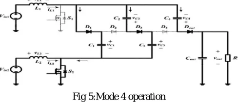
In this mode, switch S1 is OFF and S2 is ON .All the odd numbered diodes are forward biased and the inductor current IL1 flows through the VM capacitors charging the odd numbered capacitors (C1, C3, . . .) and discharging the even numbered capacitors (C2, C4, . . .). If the number of VM stages is odd, then the output diode Dout is reverse biased and the load is supplied by the output capacitor. However, if the number of VM stages is even, then the output diode is forward biased charging the output capacitor and supplying the load. In the particular case considered here, since there are four VM stages, the output diode is forward biased.
Fig 5:Mode 4 operation
Mode 3
Fig 6:Mode 3 operation
III.SOLAR ARRAY AND MPPT ALGORITHM
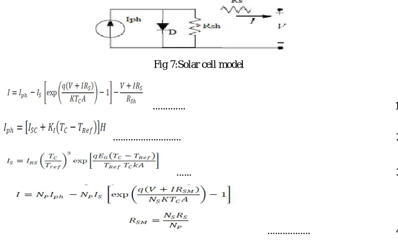
The basic structure of solar cells is to use a p-type semiconductor with a small quantity of boron atoms as the
substrate. Phosphorous atoms are then added to the substrate using high-temperature diffusion method in order to form the p-n junction. In the p-n junction, holes and electrons will be rearranged to form a potential barrier in order to prevent the motion of electrical charges. When the p-n structure is irradiated by sunlight, the energy supplied by photons will excite the electrons in the structure to produce hole-electron pairs. These electrical charges are separated by the potential barrier at the p-n junction. The electrons will move towards the n-type semiconductor and the holes will move towards the p-type semiconductor at the same time. If the n-type and p-type semiconductors of a solar cell are connected with an external circuit at this moment, the electrons in the n-type semiconductor will move to the other side through the external circuit to combine with the holes in the p-type semiconductor. The phenomenon above shows how currents of the A PV array is a group of several PV cells which are electrically connected in series and parallel circuits to generate the required current and voltage.external
circuit generate. Because the output voltage of a solar cell is extremely low (about 0.5–0.7V), solar cells have to be connected in series and in parallel in practical applications first.Fig 7:Solar cell model
... 1
... 2
... 3
... 4
Iph= light-generated current or photocurrent,
Is= cell saturation of dark current,
q= 1.6 ×10⁻¹⁹ C) is an electron charge,
Tc=the cell’s working temperature,
A= an ideal factor,
Rsh= Shunt resistance, and
Rs= series resistance of solar cell.
Isc= the cell’s short-circuit current at a 25°C and 1kW/m2,
Ki= the cell’s short-circuit current temperature coefficient,
Tref= the cell’s reference temperature, and
H= the solar insolation in kW/m2.
I rs=the cell’s reverse saturation current at a reference temperature and standard solar radiation
Eg= is the bang-gap energy of the semiconductor used in the cell
A is the ideal factor, dependent on PV technology.
MPPT Algorithm
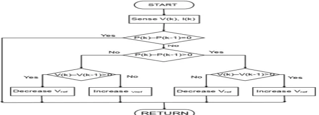
MPPT algorithms are necessary in PV applications because maximum power point of a solar panel varies with irradiation and temperature so the use of MPPT algorithm is required to obtain the maximum power from a solar array.MPPT controller can be implemented by operating on the converter duty cycle.In this paper Perturb and Observe algorithm is used. It is the simplest method and is widely used. In this technique we generally use only one sensor, that is the voltage sensor, to sense the PV module voltage and hence the cost of implementation is less and hence easy to implement without any complexity. The time complexity of this algorithm is very less for calculating the maximum power but on reaching very close to the Maximum Power Point (MPP) it doesn’t stop at the MPP and keeps on perturbing on both the directions so for that reason it have multiple local maximum at the very same point. First of all the algorithm which reads the value of the current and voltage from the photovoltaic module from that power is calculated the value of voltage and power at that instant is stored. Hence a slight perturbation is added in the increasing direction. The next values at the next instant are measured and power is again calculated. Hence by adjusting the maximum power duty cycle can be obtained based on it. In certain situations like changing atmospheric conditions and change in irradiance the maximum power point shifts from its normal operating point. In the next iteration it changes its direction and goes away from the maximum power point and results in multiple local maxima at the same point. So the maximum power point deviate from its original position.
Fig 8:Perturb and observe algorithm
IV.SINGLE PHASE INVERTER
obtained by varying the gain of the inverter, which is normally accomplished by pulse-width-modulation control within the inverter.The inverter gain can be defined as the ratio of the ac output voltage to dc input voltage.The output voltage wave forms of ideal inverters should be sinusoidal. However,the wave forms of practical inverters are nonsinusoidal and contain certain harmonics.For low and medium power applications, square wave or quasi square wave voltages may be acceptable; and for high applications, low distorted sinusoidal wave forms are required. With the availability of high speed power semiconductor devices, the harmonic contents of the output voltage can be minimized or reduced significantly by switching techniques.The DC-AC inverter consists of a full bridge inverter comprises of four switches and with a lowpass filter.PWM technique is used for driving switches. Four switches are driven by the pulse width modulation signals came from the compared result of sinusoid amplitude signal and triangle carrier.
During positive half cycle, switches S1 and S4 are active; other switches including S2 and S3 are turned on. The switch S4 is subject to duty cycle modulation control. The D is duty ratio determined by the compared results of the sinusoid amplitude control signal Vcontrol and the triangle carrier signal Vtri. When Vtri > VControl,S4 is turned on, and vice versa.The average voltage Vab among the points a and b can be derived as
During negative half cycle, switches S2 and S3 are active; other switches including S1 and S4 are turned on. The switches S3 is subject to duty cycle modulation control. When Vtri > Vcontrol, S3 is turned on, the average voltage Vab among the points a and b can be derived as:
V.DESIGN OF CONVERTER
VI.SIMULATION RESULT AND DISCUSSION
The complete simulation model of high static gain boost DC-DC converter with two input stages is shown below. In this simulation model ,one of the source is PV array and the other is battery. For the first source i.e PV array,MPPT is implemented for tracking the maximum power point so that maximum power can be obtained from the array.MPPTcontroller controls the duty cycle of the converter. Since the ouput of the PV panel is low ,high gain converters are used to interface it with the grid.Single phase inverter is used to convert the high voltage DC to AC . For tracking maximum power point, MPPT algorithm mainly perturb and observe algorithm is used.
... 7
...8
...9
...10
... 5
Fig 9:Simulink model for the new topology
Specification for PV panel is given below
Table 1:PV panel specification
Input DC voltages of 12V is given to the converter. One of the source is PV array and the other is battery.For the first source i.e PV array,MPPT is implemented for tracking the maximum power point
Fig 10:Waveform for input voltage 1
Input voltage 1 is from PV array.Input voltage from the first source is taken as 12V
Fig 11:Waveform for input voltage 2
Out of two sources,first input voltage 12V is from PV array and the second input voltage 12V is from battery.
Converter output voltage is 240V for an input voltage from two sources.The gain of the converter is found to be 20.
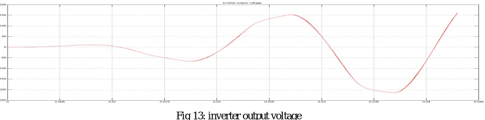
Fig 13: inverter output voltage
An AC voltage of 240V is produced from single phase inverter. The output voltage wave forms of ideal inverters should be sinusoidal. However, the wave forms of practical inverters are nonsinusoidal and contain certain harmonics.
VI.CONCLUSION
This converter is based on diode capacitor VM stages .Voltage gain is increased by increasing the number of VM stages .It can draw power from two input sources like a multiport converter or from a single source in an interleaved manner. It has the flexiblity to be connected to independent sources.So ,one of the input source is replaced with PV source. Simulation of the converter has been done successfully and its output voltage has been found to be 240V with a gain of 20 .
REFERENCES
[1] W. Li and X. He, “A family of interleaved DCDC converters deduced from a basic cell with winding-cross-coupled inductors (WCCIs) for high step-up or step-down conversions”, IEEE Trans. Power Electron., vol. 23, no. 4, pp.17911801, Jul. 2008.
[2] W. Li, Y. Zhao, Y. Deng, and X. He,” Interleaved converter with voltage multiplier cell for high step-up and high-efficiency conversion, IEEE Trans.Power Electron”., vol. 25, no. 9, pp. 23972408, Sep. 2010.
[3] Y.-P. Hsieh, J.-F. Chen, T.-J. Liang, and L.-S. Yang, “A novel high step-up DCDC converter for a microgrid system, IEEE Trans. Power Electron”., vol.26, no. 4, pp. 11271136, Apr. 2011
[4] K.-C. Tseng, C.-C. Huang, and W.-Y. Shih, “A high step-up converter with a voltage multiplier module for a photovoltaic system, IEEE Trans. Power Electron.”, vol. 28, no. 6, pp. 30473057, Jun. 2013.
[5] K.-C. Tseng and C.-C. Huang, “High step-up high-eciency interleaved converter with voltage multiplier module for renewable energy system”, IEEE Trans. Ind. Electron., vol. 61, no. 3, pp. 13111319, Mar. 2014.