International Journal of Innovative Research in Science, Engineering and Technology An ISO 3297: 2007 Certified Organization Volume 6, Special Issue 5, March 2017
National Conference on Advanced Computing, Communication and Electrical Systems - (NCACCES'17)
24th - 25th March 2017
Organized by
C. H. Mohammed Koya
KMEA Engineering College, Kerala- 683561, India
Design and Implementation of 2.4GHz MMIC
Power Amplifier Using ADS Software
Deepti S. Shastrimath1
Assistant Professor, Department of Electrical and Electronics Engineering, Dr Ambedkar Institute of Technology, Bangalore, India1
ABSTRACT: This paper contends the design of MMIC power amplifier for wireless application by using 0.15µm GaAs Power Pseudomorphic High Electron Mobility Transistor (PHEMT) technology with a gate width of 100µm and 10 fingers at 2.4GHz. The 2.4GHz power amplifier can be applied for wireless applications such as Wi-Fi and WPAN. Software ADVANCED DESIGN SYSTEM (ADS) is used to simulate schematic and layout of the power amplifier in order to obtain the best performance of the power amplifier.
KEYWORDS: Power Amplifier, MMIC, Lumped components, WIN components and ADS
I. INTRODUCTION
A Typical MMIC or RFIC design flow is to start with topology analysis with respect to specifications. Table.1: Operating conditions
Parameter Value
Vdd 2.5 to 3 V
Vbias -1 to 0 V
Impedance matched Zin/Zout 50Ω
Table.1 shows the operating conditions for the design of power amplifier at 2.4GHz.Table II shows the different parameter values to be met after the simulation of the final layout to ensure the design to be perfect.
Table.2: Parameter values
Parameter Value
Higher Linear Gain 24 dB – 30 dB
Power Gain at 1 dB Compression Point 22 dB – 29 dB
Pout at 1 dB Compression Point (P1dB) 24 dBm – 33 dBm
PAE at 1 dB Compression Point 15% – 26%
3rd order Intermodulation (IM3) (Δf = 10MHz, Pout = 17 dBm) 35 dBc – 47 dBc
High Linearity, OIP3 -
Drain Current, Idd at 1 dB Compression Point 350 mA - 1000 mA
II. BLOCKDIAGRAM
The design approach is one of the major issues in modelling any power amplifier mostly when more than one amplifier is part of the design. There are three different kinds of topologies push-pull amplifier, balanced amplifier and interstage amplifier. In this case as output power was not very high and most the important concern was to have output as linear as possible and chip size as small as possible, push-pull power amplifier designs was not taken into consideration as they are known for high output power and high efficiency. Similarly balanced power amplifiers are good choice for having low VSWR at input as well as output i.e. good matching still this configuration was not used as it will only increase both the chip size and the complexity of the circuit by adding some quadrature hybrids for having balanced signals which is at time hard to achieve, and also good matching was possible without them. Hence the new approach was implemented in interstage topology to achieve good linearity and also small size.
Fig.1: Block diagram
III. DESIGN PHILOSOPHY
The design of each sub-circuit components of the PA was first done using ideal lumped elements. Those ideal elements were replaced using the corresponding models from WIN design kit. Resistors and capacitors were easy to synthesize, but inductors had to be carefully modelled using an iterative tuning process. Connection of these WIN foundry components were accomplished using tee, taper, bend and micro-strip transmission line also available in WIN design kit.
Fig.2: Single Stage Power Amplifier Topology
Amplifier
Operating point: The Fig.3 shows the I-V characteristics when Vds is swept from 0V to 7V, but in the final stage of design the amplifier was biased at Vds = 3V ad Vgs = -0.9V.
1 Bias
Network
IMN
Fig I I-V Charactericts
Fig.3: I-V characteristics
Matching Network: The matching network was designed to work over a large bandwidth. Both input and output matching network is designed for amplifier.
Biasing Network: The biasing network includes DC feed and DC blocks in parallel leading to the ground. After tuning and optimizing the circuit this DC feed and block at the gate bias became the part of the matching network.
Feedback Loop Circuitry: The transistor PHEMT was provided with feedback with a resistor and a capacitor. The capacitor is used to block the DC through the feedback it reduces the power added efficiency but less power is wasted by thermal dissipation. The main purpose includes this feedback network is to stabilize the output.
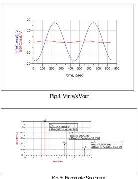
Results: The result are observed in the below figures. The output power obtained was above the required and well within the linear region so the driver stage gave a high gain which made the task easier for the amplifier to produce required output power within the linear region with less clipping in the output voltage.
Fig.4: Vin v/s Vout
Fig.5: Harmonic Spectrum
The output voltage (Vout) is shown in the |Fig.5 for fundamental harmonics and as we can see second harmonics are well suppressed to -31dB compared to the fundamental.
100 200 300 400 500 600 700 800
0 900 -10 0 10 -20 20 time, psec ts (A C .v in ), V ts (A C .v o u t) , V
1 2 3 4 5 6 7
0 8 -40 -30 -20 -10 0 -50 10 freq, GHz d B m (H B .V o u t) m1 m2 m3 m1 freq= dBm(HB.Vout)=8.5432.400GHz m2 freq= dBm(HB.Vout)=-31.7284.800GHz m3 freq= dBm(HB.Vout)=-40.1797.200GHz
1 2 3 4 5 6
IV.POWER AMPLIFIER CIRCUIT
After the design for amplifier was completed, the following job was just to build a schematic including lumped components. Input impedance and output impedance of the amplifier are measured in ADS and matching network is designed using lumped-elements. Lumped elements are replaced with WIN components in the matching network. Good results are observed after tuning the matching network consisting of capacitors and inductors. Table.3 shows the observed results after testing the pre-layout schematics. Micro-strip line, tee and m-corn, are used and better simulation results can be observed after tuning of the post-layout, which can be seen in Table.3 compared with pre-layout.
Table.3: Summary of power amplifier performance
Parameter Post-layout
S(11) -10.5
S(22) -9.65
S(12) -15.82
S(21) 8.39
Stability factor 1.23
V. SCHEMATIC RESULTS
When the amplifier stage is connected with the micro-strip transmission lines, tee and M-corn the entire power amplifier can be simulated for small signal and large signal performance.
Fig.6: Stability Factor
Fig.8 shows the power amplifier is unconditionally stable over the bandwidth.
Fig.7: S parameters
1.5 2.0 2.5 3.0 3.5
1.0 4.0 1.5 2.0 2.5 3.0 1.0 3.5 freq, GHz S ta b F a c t1 m6 m6 freq= StabFact1=1.235 2.400GHz
1.5 2.0 2.5 3.0 3.5
The simulated performance of the amplifier was very encouraging. Fig VIII shows the s-parameters for the amplifier.
VI. FINALLAYOUT
We use PHEMT process which is based on a 100µm GaAs substrate thickness. The layout is shown in Fig.9.
Fig.8: Final Layout of Two Stage Amplifier
The main features of the layout are
Tee
M corn
Air bridge capacitor
Round air bridge cross inductor
Square air bridge cross inductor
TFR (Thin Film Resistor)
MESA resistor
Double metal micro strip line
VII. TEST PLAN
In order to measure the power amplifier after WIN foundry fabrication it is necessary to place DC needle probes to provide individual bias to the gate and drain of the transistor, RF probes will come in from the top and left side of the chip for input and output, respectively.
VIII. CONCLUSION
After the successful completion of design, the following conclusion is observed.
application by using 0.15μm GaAs Power Pseudomorphic High Electron Mobility Transistor (PHEMT) technology with a gate width of 100μm and 10 fingers. Software ADS was used in the designing process.It has been demonstrated
that at a 3.0 V drain voltage, the amplifier has achieved 17.265 dB small-signal gain S21, input and output return loss of 16.310 dB and 14.418 dB, P1dB of 14.862dBm with 12.318% power-added efficiency (PAE) for 2.4 GHz power amplifier. The designed MPA are in unconditionally stable condition due to the stability factor for the MPA are higher than 1 at the whole range of frequency. The die sizes of the amplifiers from the layout design are 1mm x 2.08mm MPA respectively.
IX. FUTURE SCOPE
The design of single-stage amplifier can be extended to two-stage amplifier design to meet the specification still more efficiently. In order to improve the performance of the system and achieve a higher output power, the matching system should be designed in a specific way. So an interesting future work would be to improve the ADS model of the transistor by extracting its parameters and bias characteristics and then to redesign the power amplifier which should lead to a good improvement in the power performance.
REFERENCES
[1] Agilent Technologies. (2005). Agilent ADS 2005A. Momentum.
[2] Brattain, W. H. (1968, March). Genesis of the Transistor. The Physics Teacher, 109–114.doi:10.1119/1.2352401
[3] Chu, C. K., Huang, H. K., Wang, C. C., Wang, Y. H., Hsu, C. C., Wu, W., et al. (2004). A 3.3 V selfbiased 2.4–2.5 GHz high linearity PHEMT
MMIC power amplifier. In Proceedings of the 29th European Solid-State Circuits Conference, 2003 (pp. 667-670).
[4] Cortese, P., Akkul, M., Mayockl, J., Pilcherl, I., & Sanhaml, J. (2006). 3.5Ghz 10-Watt Power Amplifier for WiMax Application. In The 9th
European Conference on Wireless Technology, 2006 (pp. 182-184).
[5] Cripps, S. C. (1983). A theory for the prediction of GaAs FET load-pull power contours. 1983 IEEE MTT-S International Microwave
Symposium Digest (pp. 221-223).
[6] Cripps, S. C. (1999). RF Power Amplifier for Wireless Communications (pp. 45–72). Artech House, Inc.
[7] Deukhyoun, A. R. H., Moonkyun, M., Sutono, A., Kyutae, L., & Laskar, J. (2002). A 2.2-V operation,2.4-GHz single-chip GaAs MMIC
transceiver for wireless applications. 2002. IEEE MTT-S International Microwave Symposium Digest. IEEE MTT-S International Microwave Symposium, 2, 1019–1022.
[8] Edwards, T.C. & Wiley, J. (1987). Foundations of Microstrip Circuit Design. Golio, M. (2001). The RF and Microwave Handbook. Boca
Raton, FL: CRC Press LLC.
[9] Kang, D. M., Lee, J. H., Yoon, H. S., Kim, S. J., Shim, J. Y., & Lee, K. H. (2002). Wideband 36- to 44- GHz MMIC Power Amplifier Using a