Available Online at www.ijpret.com 129
INTERNATIONAL JOURNAL OF PURE AND
APPLIED RESEARCH IN ENGINEERING AND
TECHNOLOGY
A PATH FOR HORIZING YOUR INNOVATIVE WORK
IMPLEMENTATION OF I2C PROTOCOL USING FPGA
BHUSHAN A. SAWALKAR, N. N. KASAT
Electronics and Telecommunication, Sipna College of Engineering and Technology, Amravati, India Accepted Date: 15/03/2016; Published Date: 01/05/2016
\
Abstract: We present design of an inter-integrated circuit (I2C) bus protocol. It also gives
excellent speed compared to other protocols. I2C uses only two wire for communication. It is light weight, economical and omnipresent. It also increases data transfer rate. To enable multiple devices to communicate with each other over serial data bus without any data or address loss, as well as to enable faster devices with slower ones. This protocol design proposed for reusability concept. In this paper, a design on FPGA Platform is presented for IP2C protocol. Also proposed model is used for communication between masters and multiple slaves. The entire design has been coded in VHDL & verified using Altera kit.
Key Words: I2C, VHDL, FPGA.
Corresponding Author: MR. BHUSHAN A. SAWALKAR Access Online On:
www.ijpret.com How to Cite This Article:
Available Online at www.ijpret.com 130 INTRODUCTION
The physical size and power requirement of IC get reduce over the years. The main reason for that is more number of transistors can be integrated into smaller size and less number of interconnections wire present in between ICs can possible. The actual circuitry of the IC is much smaller than the packaging of the IC but it requires larger area to cover because of interconnection wire present in between ICs. The bus protocol which manages the communication between the ICs within a system and between the systems is called the Inter-IC bus or I2C bus. In the world of multiple application based product it is very much a mandatory to have multiple devices connected to a system, this includes peripherals following different communication protocols as well. This requirement give rise to the need for an intermediate system which can act as a bridge between two or more devices following different communication protocols. This is where I2C master protocol design is very useful.
THEORY RELATED WORK
1. I2C Protocol
The I2C system uses a serial data line (SDA) and a serial clock line (SCL) for data transfers. All devices connected to these two signals must have open drain or open collector outputs. The logic AND function is exercised on both lines with external pull-up resistors.
I2C Addressing Format
The various devices on the I2C bus can be differentiated by their address. It contains 10 bit
addressing mode. Its 1st master send start/repeated start condition, 2nd step, master send 7 bit
of particular slave device address out of many devices.3rd step, if bit indicate 1 for read and 0
for write bit respectively. Then 4th step, acknowledgement bit indicate that slave device address
received successfully.5th step, master sends data to slave device. 6th step master received
acknowledgement and then master sends a stop condition that indicate no more data or address will there. Finally stop the transaction.
Figure 1: Data Transfer on the I2C Bus S A7 A6 A5 A4 A3 A2 A1 RW ACK D7 D6 D5 D4 D3 D2 D1 D0 NACK P SCL
SDA
1 2 3 4 5 6 7 8 9
MSB LSB
1 2 3 4 5 6 7 8 9
Available Online at www.ijpret.com 131 Start & Stop Condition
Every data/address transfer in this protocol first requirement is start condition. START condition indicates that SCL must be high state. And SDA line must follow the transition from High to Low. Initially both are at high impedance (Z) and for STOP condition indicate that SCL must be high state. And SDA line must follow the transition from Low to High.
Acknowledgement
Master/slave receivers pull data line low for one clock pulse after reception of a byte. Master receiver leaves data line high after receipt of the last byte requested. Slave receiver leaves data line high on the byte following the last byte it can accept. Receiver leaves data line high for one clock pulse after reception of a byte.
Arbitration
InI2C protocol, only master can involve in arbitration. Slaves are not involved in arbitration. Master initiate transfer only and only when bus is idle. Two masters may initiate a START condition within the minimum hold time of the I2C bus START condition for which gives in a valid START condition on it. Arbitration is needed to check which master will complete their transmission as early as possible. There is no data lost in it. The advantage is that two master can complete its transmission without causing any hazard or error. Arbitration procedure keeps sending pattern bit by bit. When the SCL is gone high it will also verify SDA level for which is sent. For the first time a master try to initiates or generate a HIGH period, but that will be detecting the SDA level also gone LOW, the master knows that it will be lost the arbitration procedure and turns off its SDA output driver. Another master goes to finish their entire transaction.
2. FPGA – Field Programmable Gate Array
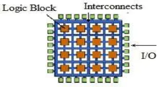
A field-programmable gate array (FPGA) is an integrated circuit designed to be configured by a customer or a designer after manufacturing – hence "field-programmable". The FPGA configuration is generally specified using a hardware description language (HDL).FPGAs contain an array of programmable logic blocks, and a hierarchy of reconfigurable interconnects that allow the blocks to be "wired together", like many logic gates that can be inter-wired in different configurations. Logic blocks can be configured to perform complex combinational
functiorns, or merely simple logic gates like AND and XOR. In most FPGAs, logic blocks also
Available Online at www.ijpret.com 132 Figure 2: FPGA block diagram
CLB
The heart of the FPGA lies in the CLBs. CLBs appear in rows and columns within all
FPGAs and implement the logic functions desired by the programmer. Most CLBs accomplish this with a lookup table. Lookup tables (LUTs) are digital memory arrays that contain truth tables for any logic function that can be implemented by the given number of logic inputs for a CLB. The output of the CLB is then the logical result of the function recorded in the lookup table. In order to program the CLBs, truth tables be loaded into the LUTs of each CLB.
Interconnect
While the CLB provides the logic capability, flexible interconnect routing routes the signals between CLBs and to and from I/Os. Routing comes in several flavors, from that designed to interconnect between CLBs to fast horizontal and vertical long lines spanning the device to global low-skew routing for Clocking and other global signals. The design software makes the inter-connect routing task hidden to the user unless specified otherwise, thus significantly reducing design complexity.
I/O
I/O blocks provide for interaction with the outside world. An I/O pin can be used for input or output. I/O blocks can contain logic functionality, although high logic utilization decreases pin placement flexibility, as I/O blocks utilized in logic cannot be reassigned mid-design.
Today’s FPGAs provide support for dozens of I/O standards thus providing the ideal interface bridge in your system. I/O in FPGAs is grouped in banks with each bank independently able to support different I/O standards. Today’s leading FPGAs provide over a dozen I/O banks, thus allowing flexibility in I/O support.
Available Online at www.ijpret.com 133 LITERATURE SURVEY
The I2C bus was developed in the early 1980's by Philips Semiconductors. Its original purpose was to provide an easy way to connect a CPU to peripheral chips in a TV-set. Peripheral devices in embedded systems are often connected to the MCU as memory-mapped I/O devices, using the microcontroller's parallel address and data bus. This result in lots of wiring on the PCB's to route the address and data lines, not to mention a number of address decoders and glue logic to connect everything. In mass production items such as TV-sets, VCR's and audio equipment, this is not acceptable. In these appliances, every component that can be saved means increased profitability for the manufacturer and more affordable products for the end customer. Furthermore, lots of control lines implies that the system is more susceptible to disturbances by Electromagnetic Interference (EMI) and Electrostatic Discharge (ESD). The research done by Philips Labs in Eindhoven (The Netherlands) to overcome these problems resulted in a 2-wire communication bus called the I2C bus. I2C is an acronym for Inter-IC bus. Its name literally explains its purpose: to provide a communication link between Integrated Circuits. Today, the I2C bus is used in many other application fields than just audio and video equipment. The bus is generally accepted in the industry as a de-facto standard. The I2C bus has been adopted by several leading chip manufacturers like Xicor, ST Microelectronics, Infineon Technologies, Intel, Texas Instruments, Maxim, Atmel, Analog Devices and others [2].
Several competitors, such as Siemens AG (later Infineon Technologies AG, now Intel mobile communications), NEC, Texas Instruments, STMicroelectronics (formerly SGS-Thomson), Motorola (later Freescale), and Intersil have introduced compatible I2C products to the market since the mid-1990s. SMBus, defined by Intel in 1995, is a subset of I2C that defines the protocols more strictly. One purpose of SMBus is to promote robustness and interoperability. Accordingly, modern I2C systems incorporate policies and rules from SMBus, sometimes supporting both I2C and SMBus, requiring only minimal reconfiguration. Since October 10, 2006, no licensing fees are required to implement the I2C protocol. However, fees are still required to obtain I2C slave addresses allocated by NXP [3]. Zheng-wei HU, I2C Protocol Design for Reusability: Third International Symposium on Information Processing –In this paper I2C protocol design method for reusability was proposed. In this method, design was divided into 3 levels: protocol level, signal level and interface level. The design method was design in VHDL, implemented in FPGA and applied in bio-logging design for RTC and light sensor which are based on I2C protocol. The data acquired by light sensor were transferred through RS232 to PC and stored into text file. The file was shown into graph by using Matlab. The data acquired by
Available Online at www.ijpret.com 134 master controller on FPGA using VHDL,” IJET, Aug-Sep 2012, the focus of this paper is on I2C protocol following master controller. This controller is connected to a microprocessor or computer and reads 8 bit instructions following I2C protocol. 32 bit register is designed to send data serially as per SPI instructions. The complete module is designed in VHDL and simulated in ModelSIM. This concept is widely applicable where a microprocessor wants to communicate
with SPI device [5]. A.K. Oudjida, M.L. Berrandjia, R. Tiar, A. Liacha, K. Tahraoui “FPGA
Implementation of I2C& SPI Protocols” a Comparative Study IEEE 2009 I2C and SPI are the most commonly used serial protocols for both inter-chip and intra-chip low/medium bandwidth data-transfers. This paper contrasts and compares physical implementation aspects of the two protocols through a number of recent Xilinx’s FPGA families, showing up which protocol features are responsible of substantial area overhead. This valuable information helps designers to make careful and tightly tailored architecture decisions. For a comprehensive comparative study, both protocols are implemented as general purpose IP solutions, incorporating all necessary features required by modern ASIC/SoC applications according to a recent market investigation of an important number of commercial I2C and SPI devices. The RTL code is technology independent, inducing around 25% are overhead for I2C over SPI, and almost the
same delays for both designs [6]. Arvind Sahu, Ravi Shankar Mishra, Puran Gour, Design and
Interfacing of High speed model of FPGA using I2C protocol: Int. J. Comp. Tech. Appl., Vol 2 (3), 531-536 ISSN:2229-6093. Sahu et al. developed inter IC protocol for data surveillance purpose. Data surveillance is very important application to monitor people or sensors.I2C is used for data surveillance because it could make system efficient, accurate, flexibility, and low development cost. They designed a protocol in VHDL and interface with OV7620 single chip CMOS VGA color digital camera. Data surveillance includes monitoring people or collection of sensors information from various nodes. They developed system which will replace traditional cameras with LAN cameras with complex image processing and IP routing. Data compression takes place with H.263 algorithm due to its high compression efficiency and high data rate. For surveillance constant bit rate limit the real time communication of cameras so variable bit rate is used. Variable bit rate efficiently uses available bandwidth.H.263 encoding is very complex normal DSP processor cannot handle it so FPGA as programmable solution is used. All results were verified using Modelsim and FPGA can be used as interface in between camera and local
monitor system [7]. Madhuri Daware, Prof. A. S. Patil: IMPLEMENTATION OF I2C BUS
Available Online at www.ijpret.com 135 ,“Design And Implementation Of FPGA Based Interface Model for Scale Free Network Using I2C Bus Protocol On Quartus II 6.0”, International conference on computer and devices for communication and Devices for Communication 2009. Researcher developed an interface model for scale free network using inter-IC bus protocol which includes master and slave design. Master was made up of different blocks as initiator, address block, write block, read block, clock generator. Initiator tested whether data bus was free to use or not. Address bit was transmitted by address block bit by bit to SDA line and after completion of address it reset SDA line to high position. Transmission and reception functions were performed by write and read block. All functions of master are governed by clock generator block. Slave was made up of design of monitor, address block, receiver and transmitter. Monitor function was same as initiator in master which sense the SCL and SDA line whether it is in use or not. Other blocks were functioned same as master block. Quartus II 6.0 was used to create VHDL model while it is simulated in Stratix II [9].
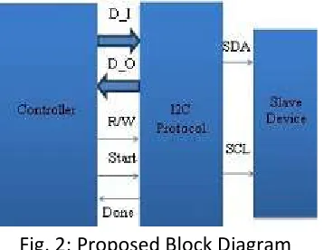
PROPOSED METHODOLOGY
In our proposed design there are basically two parts of system. One is master and second is slave. We are designing only master part of system. The I2C system uses a serial data line (SDA) and a serial clock line (SCL) for data transfers. All devices connected to these two signals must have open drain or open collector outputs. The logic AND function is exercised on both lines with external pull-up resistors. Here, we will design the master part such that our system is capable for reuse. We will use the prebuild slave device for communication with master device. Slave device may be an ADC, a DAC, Memory (RAM, SDRAM, Flash, EEROM, etc.), LCD or any other device. Here we are using memory device for implementation as a slave.
Fig. 2: Proposed Block Diagram
Available Online at www.ijpret.com 136 RESULT AND CONCLUSION
The ideal I2C bus has high performance, flexibility and low cost. The proposed method is designed in VHDL, we used the FSM design technique here and we have created the model in FPGA, so it will allow rapid prototyping of the interface model for large scale communication. We got some results and we are trying to improve it.
REFERENCES
1. The I2C-bus specification, version 2.1, January 2000, Philips Semiconductors.
2.
http://www.esacademy.com/en/library/technical-articles-and-documents/miscellaneous/i2c-bus/general-introduction/history-of-the-i2c-bus.html.
3. https://en.wikipedia.org/wiki/I2C.
4. Zheng-wei HU, I2C Protocol Design for Reusability: Third International Symposium on
Information Processing.
5. Prof. Jai Karan Singh et al “Design and Implementation of I2C master controller on FPGA
using VHDL,” IJET, Aug-Sep 2012.
6. A. K. Oudjida, M.L. Berrandjia, R. Tiar, A. Liacha, K. Tahraoui “FPGA Implementation of I2C&
SPI Protocols” a Comparative Study IEEE 2009.
7. Arvind Sahu, Ravi Shankar Mishra, Puran Gour, Design and Interfacing of High speed model
of FPGA using I2C protocol :Int. J. Comp. Tech. Appl., Vol 2 (3), 531-536 ISSN:2229-6093.
8. Madhuri Daware, Prof. A. S. Patil: IMPLEMENTATION OF I2C BUS PROTOCOL ON FPGA,
Technical Research Org. India, ISSN (Print): 2393-8374. Vol-2, issue-8, 2015.
9. Prof. P. Venkateswaran, A. Saynal, S. Das, S.K Saynal and R. Nandi , “FPGA Based Efficient
Interface Model for Scale-Free Computer Networking using I2CProtocol” 15th.intl‟conf on computing – CIC 2006, Proc. Research in Computing Science: Special Issues – Advances in Computer Science &Eng., ISSN 1870 – 406, pub. National Polytechnic Institute, Mexico, Vol.23, Nov. 21-24,2006.
10. Regu Archana, Mr. J. V. Rao, Implementation of I2C Master Bus Protocol on FPGA: Int.
Journal of Engineering Research and Applications ISSN: 2248-9622, Vol. 4, Issue 10 (Version 5), October 2014, pp.06-10.
11. B. Santosh Kumar, L. Ravi Chandra, A. L. G. N. Aditya, Fazal Noor Basha, T. Praveen
Blessington, Design and Functional Verification of I2C Master Core using OVM: International Journal of Soft Computing and Engineering (IJSCE) ISSN: 2231-2307, Volume-2, Issue-2, May 2012.
12. F. Leens, “An Introduction to I2C and SPI Protocols,” IEEE Instrumentation & Measurement