Quasi Z-source NPC Inverter for PV Application
Francis B. Effah
Dept. Electrical & Electronic Engineering Kwame Nkrumah University of Science &Technology
Kumasi, Ghana [email protected]
Patrick W. Wheeler, Alan J. Watson, Jon C. Clare Dept. of Electrical and Electronic Engineering
The University of Nottingham NG7 2RD
Nottingham United Kingdom
Abstract—This paper presents the operating principles and modified space vector modulation strategy for a three-phase quasi Z-source neutral point clamped inverter for solar photovoltaic applications. This topology combines the advantages of the neutral point clamped and quasi Z-source inverters. These advantages include single-stage buck-boost power conversion, continuous input current, and low voltage stress of switches. Simulation results are presented to verify the presented concepts.
Index Terms—Buck-boost, quasi Z-source network, single-stage, neutral point clamped, space vector modulation.
I.INTRODUCTION
In the last few years renewable energy has experienced one of the largest growth areas compared with fossil fuel energy. This is due to the increasing environmental concerns and the need for more electrical energy by emerging economies. Thus, the importance of renewable energy sources in the future energy scenario is very critical. Wind turbines, solar photovoltaic (PV), and fuel cell are the most popular renewable sources. Wind energy is leading the pack whiles solar PV is trying to catch up. A common concern shared by these renewable sources is their unstable operation that depends on several factors.
Power electronics converters is a technology that enables the efficient and flexible interconnection of different sources to the electric power system. These converters are to provide stable output voltage in spite of unstable input variables at the highest efficiency, lowest cost and minimum size. This has led to the development of many new interface power electronics converters. Most of the power converter topologies employed in PV applications are characterized as two-stage converters. The two-stage converter topology uses a boost dc/dc converter to minimize the required kVA rating of the inverter and boost the wide range input voltage to a constant desired output value [1]. However, this solution is more complex and difficult to control because of the two-stage power conversion.
A single-stage inverter is an attractive approach due to its compactness, low cost, and reliability. However, the conventional structure of a single-stage converter must be oversized to cope with the wide PV voltage variation derived from changes of irradiance and temperature [2]. Another solution is based on the intermediate Z-source network, classified as single-stage Z-source inverter [3]. This converter achieves voltage buck-boost in a single power conversion stage. Several review papers have been published in the
literature [4-5] with some reported on PV system applications [6-7]. The Z-source converter is able to handle the PV voltage variations over a wide range without overrating the converter. Thus, the component count and system cost are reduced, with improved reliability because of the allowed shoot through state [8]. A variant of the Z-source converter proposed relatively recently is the quasi Z-source inverter [9]. This converter has some new attractive advantages more suitable for PV applications [10].
This paper presents a modified modulation strategy for the three-phase quasi Z-source neutral point clamped (qZNPC) inverter with enhanced output voltage waveform. This converter is intended for applications that require a wide operation range of input voltage as well as continuous input current. It must be stated that other authors [10] have considered this converter in previous work. However, the modulation strategy employed in this paper is different and ensures the output voltages fed to the grid are of enhanced quality.
The rest of the paper is organized as follows. Section II describes in detail the operating principles and steady state analysis of the qZNPC inverter. Section III presents the modified space vector modulation strategy developed to distribute shoot-through states to enable a boost functionality. Simulation results are presented in section IV.
II.OPERATING PRINCIPLES OF QUASI Z-SOURCE NPC
INVERTER
The quasi Z-source inverter was derived from the traditional Z-source inverter for enhanced performance. All the advantages of the Z-source inverter are inherited by the quasi Z-source inverter [11]. The use of this new topology ensures the inverter draws constant current from the PV array and is capable of handling a wide input voltage range [12]. It also employs lower rated components, reduces switching ripples to the PV panels, and suffers less EMI problems compared to the conventional Z-source inverter.
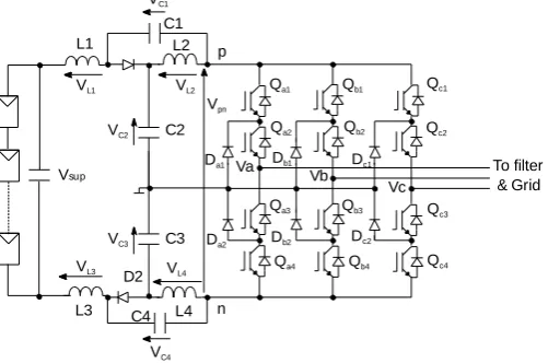
inverter combines the advantages of the quasi Z-source and NPC inverters. Figure 1 illustrates the topology of the qZNPC inverter. The PV string is coupled to the inverter by the quasi Z-source network. Each leg of the inverter circuit is composed of four switches with antiparallel diodes. Each phase generates three output voltage levels: -Vpn/2, 0, Vpn/2. Taking all three
phases into account, the converter has a total of 27 valid switching states.
Due to the presence of the quasi Z-source network, shoot through states can be added in each phase leg. During shoot through states, energy is stored in the inductors and transferred to the capacitors and load during the non-shoot through states. Consequently, the peak dc-link voltage is controlled by adjusting the shoot-though duty cycle. These shoot through states are forbidden in conventional NPC inverter because they would cause a short circuit of the dc-side capacitors. The preferred shoot through states for this converter are the upper-shoot-through (UST) and lower-upper-shoot-through (LST) states because these give rise to enhanced output voltages. The line-to-line voltages resulting from this control method have adjacent level switching with lower total harmonic distortion (THD) compared to the full shoot-through strategy employed by other authors. An UST state occurs when the three upper switches in a phase leg are turned on simultaneously while LST state refers to the simultaneous turn on of the bottom three switches in a phase leg.
VC1
C1
VL2
VL1
L1 L2
L3 VL3
D2 VL4
Qa1 Qb1 Qc1
Qa2
Qa3
Qa4
Qb2
Qb3
Qb4
Qc2
Qc3
Qc4
Da1 Db1 Dc1
Da2 Db2 Dc2
Va
Vb
Vc C2
C3 VC3
VC2
Vpn
p
n L4 C4
VC4
Vsup To filter
[image:2.595.39.290.357.523.2]& Grid
Fig. 1 Quasi Z-source NPC inverter
The behavior of the qZNPC inverter can be represented by three equivalent circuits as shown in Fig. 2. All the switching states can be separated into three modes: non-shoot through (NST) states comprising active and zero states of the conventional NPC inverter (Fig. 2a), UST states (Fig. 2b) and LST states (Fig. 2c). Assuming that the quasi Z-source network is symmetric, we have L1 = L3, L2 = L4 and C1 = C4,
C2 = C3. Accordingly, the voltages across the passive
components are VL1 = VL3, VL2 = VL4, and VC1 = VC4, VC2 =
VC3.
L1 L2
C1
VL2
VL1
VC1
C2
C3 VC2
VC3
L4 C4 L3
VL3 VL4
VC4
Vsup
(a)
L1 L2
C1
L3 C4 L4
VC4
VL4
VL3
VL1 VL2
VC1
C2
C3 VC3
VC2
0 Vsup
(b)
L1 L2
C1
L3 C4 L4
VC4
VL4
C3 C2
VL3
VC3
VC2
VL2
VL1
VC1
0 Vsup
(c)
Fig.2. Simplified representation of qZNPC inverter in (a) NST, (b) UST, and
(c) LST states.
It is assumed that the converter operates in the continuous conduction mode. The operation of the converter in this mode is given by
1
U L
N D D
where DN, DU and DL represent the duty cycles of the NST,
UST and LST states, respectively. To ensure symmetric operation, DU and DL are set to be equal and represented by D0.
The peak of the dc-link voltage is given by the sum of the capacitor voltages, as
pn C C C
C V V V V
V1 2 3 4 . (2)
In Eq. 2, VC1, VC2, VC3, and VC4 represent the average capacitor
voltages over a switching period. The voltages on the capacitors are found from the voltage balance of the inductors over a switching period as
0 sup 0 4 1
4
2 D
V D V
VC C
, (3)
0 sup 0 3
2
4 2
) 1 (
D V D V
VC C
. (4)
Thus the peak dc-link voltage is given by
0 sup
2
1 D
V Vpn
. (5)
And the peak output line-to-line voltage is found as
sup
sup 0
2 1
1
V M B V D M
Vout F
, (6)
where BF is the boost factor and M is the modulation index,
respectively.
III.MODIFIED SVM FOR QUASI Z-SOURCE INVERTER
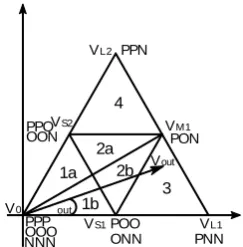
Space vector modulation (SVM) is a pulse-width modulation (PWM) strategy that uses the concept of space vectors to compute the duty cycles of the switches. The operation of each phase leg of a conventional NPC inverter can be represented by three switching states P, O, and N. The 27 switching states of the NPC inverter define 19 space vectors distributed over six sectors. Fig. 3 shows the space vector diagram for sector I. The rotating reference vector
out
V represents the desired three-phase output voltage.
Vout
V0
PPP VS1
OOO NNN
POO ONN
VL1
PNN
VM1
PON VS2
PPO OON
VL2 PPN
4
3 1a
1b 2a
2b
[image:3.595.37.264.210.384.2]out
Fig. 3 Space vector diagram for sector I of a conventional NPC inverter
The SVM for the NPC inverter is based on the “volt-second balancing” principle; that is, the product of the reference
voltage and the sampling period equals the sum of the voltage multiplied by the time interval of chosen space vectors. The “volt-second balancing” principle enables us to calculate the duty cycle of the various space vectors over a switching period.
The modulation process is completed by applying the selected voltage vectors to the output according to a switching sequence. A switching sequence that gives minimum number of switching transitions and high quality output waveform is the preferred choice. In order to achieve minimum number of switching transitions, a 7-segment switching sequence is usually adopted in SVM.
It is convenient to perform “origin shifting” and subsequently perform a three-level modulation using two-level principles [16-17]. In Fig.3, if the origin is shifted from {PPP/OOO/NNN} to {POO/ONN}, the equivalent null (E-null) state is transferred to {POO/ONN} while the equivalent active (E-active) states are transferred to {PPP/OOO/NNN}, {PPO/OON}, PON and PNN, respectively. The sequence over time of the application of the selected converter switching states has to be decided for every switching cycle. For instance in triangle 3 the voltage vectors VS1, VM1, and VL1 are
selected to synthesize the reference
out
V so the switching sequence used is ONNPNNPONPOO.
In order to achieve boost functionality for the qZNPC inverter, shoot-through states are inserted into the appropriate phase legs. Upper shoot through states (U) are inserted in phases with an “O” state with the other two phases having states of either “O” or “N” in order to get the correct line-to-line voltages. In like manner, LST states (L) are inserted in phases with an “O” state with the adjacent phases being of either state “O” or “P” [18]. It is clear from above that the “U” and “L” states need to be deployed in an optimal way that does not increase the number of commutations. Thus, a modified PWM sequence which achieves this can be derived.
[image:3.595.106.228.548.672.2]The 7-segment PWM switching pattern for modulating a conventional NPC inverter and the qZNPC inverter is shown in Fig. 4. It is clear that the “U” and “L” states are inserted in the E-null states to obtain a boost functionality in the qZNPC inverter. However, the appropriate UST and LST states have to be used otherwise there will be a collapse in the line-to-line voltages.
0.5Tu 0.5Tl 0.5Tl 0.5Tu
ONN PNN PON POO PON PNN ONN
ONN UNN PNN PON POL POO POL PON PNN UNN ONN
Tsw/2 Tsw/2
[image:3.595.308.539.552.615.2]Tsw
Fig. 4 PWM switching pattern for controlling qZNPC inverter
IV.SIMULATION RESULTS
0 1000 2000 3000 4000 5000 6000 7000 8000 9000 10000 0 100 200 300 400 500 600 X: 50 Y: 547.2 Frequency (Hz) L in e -t o -l in e V o lt a g e ( V ) (a)
0 1000 2000 3000 4000 5000 6000 7000 8000 9000 10000 0 100 200 300 400 500 600 X: 50 Y: 549 Frequency (Hz) L in e -t o -l in e V o lt a g e ( V ) (a)
0.1 0.11 0.12 0.13 0.14 0.15 0.16 0.17 0.18 -800 -600 -400 -200 0 200 400 600 800 Time (s) L in e -t o -l in e v o lt a g e ( V ) (b)
0.1 0.11 0.12 0.13 0.14 0.15 0.16 0.17 0.18 -800 -600 -400 -200 0 200 400 600 800 Time (s) L in e -t o -l in e v o lt a g e ( V ) (b)
0.1 0.11 0.12 0.13 0.14 0.15 0.16 0.17 0.18 -20 -15 -10 -5 0 5 10 15 20 Time (s) G ri d c u rr e n ts ( A ) (c)
0.1 0.11 0.12 0.13 0.14 0.15 0.16 0.17 0.18 -20 -15 -10 -5 0 5 10 15 20 Time (s) G ri d c u rr e n ts ( A ) (c)
0.1 0.11 0.12 0.13 0.14 0.15 0.16 0.17 0.18 0 5 10 15 20 25 Time (s) In p u t c u rr e n t (A ) (d)
0.1 0.11 0.12 0.13 0.14 0.15 0.16 0.17 0.18 0 5 10 15 20 25 Time (s) In p u t c u rr e n t (A ) (d)
0.1 0.11 0.12 0.13 0.14 0.15 0.16 0.17 0.18 -50 0 50 100 150 200 250 300 350 Time (s) C a p a c it o r v o lt a g e s ( V ) Vc2, Vc3 Vc1,Vc4 (e)
0.1 0.11 0.12 0.13 0.14 0.15 0.16 0.17 0.18 -50 0 50 100 150 200 250 300 350 X: 0.1557 Y: 275.4 Time (s) C a p a c it o r v o lt a g e s ( V ) Vc1, Vc4 Vc2, Vc3 (e)
0.1 0.11 0.12 0.13 0.14 0.15 0.16 0.17 0.18 0 100 200 300 400 500 600 700 800 Time (s) D C -l in k v o lt a g e ( V ) (f)
[image:4.595.337.516.49.691.2]0.1 0.11 0.12 0.13 0.14 0.15 0.16 0.17 0.18 0 100 200 300 400 500 600 700 800 Time (s) D C -l in k v o lt a g e ( V ) (f)
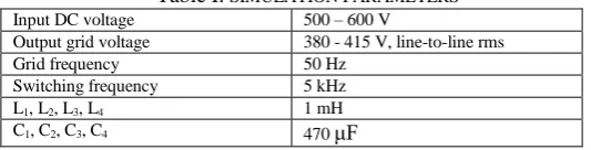
[image:4.595.67.252.52.708.2]Table I. SIMULATION PARAMETERS
Input DC voltage 500 – 600 V
Output grid voltage 380 - 415 V, line-to-line rms
Grid frequency 50 Hz
Switching frequency 5 kHz
L1, L2, L3, L4 1 mH
C1, C2, C3, C4 470 μF
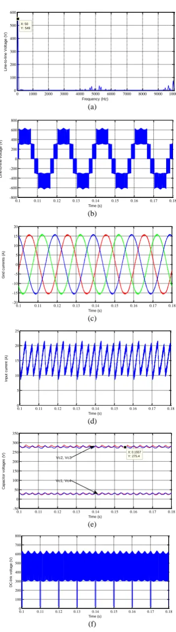
Figure 5 shows several simulation results for the case where the output of the PV array is assumed to be at the maximum of 600 V. The solar inverter therefore works in the VSI mode. To synthesize the required output voltage to the grid, a modulation index of 0.915 and D0 of 0 were used. This
operation gives a peak output line-to-line voltage of 547 V (387 V rms) as expected. This is shown in Fig. 5a. The output line-to-line voltage waveform which has adjacent level switching is shown in Fig. 5b; Fig. 5c – displays balanced output currents fed to the grid; Fig. 5d – shows the current drawn from the PV array which is without ripples because shoot-through states have not been activated; Fig. 5e – shows the capacitor voltages on C1, C4 and C2, C3 which are zero and
300 V, respectively; Fig. 5f – shows the dc-link voltage at the output of the quasi Z-source network.
To illustrate the effectiveness of the SVM algorithm described above for controlling the qZNPC to perform boost operation, it was assumed that the PV array’s voltage drops to the minimum of 500 V as a result of bad weather. In order to synthesize the required grid voltages, the output voltage of the PV array has to be boosted. This is achieved by setting the modulation index and shoot-through ratio to 0.9 and 0.1, respectively. Figure 6 depicts the main waveforms obtained when shoot-through states are used. The spectrum of the output line-to-line voltage is shown in Fig. 6a. This figure clearly shows a fundamental peak line-to-line voltage of 549 V as expected. The waveforms for the output line-to-line voltage with adjacent level switching is clearly shown in Fig. 6b. Figure 6c shows the output currents of the solar inverter which are still balanced and sinusoidal even when shoot-through states are inserted. The current drawn from the PV array during this operating mode is shown in Fig. 6d. This current is continuous with ripples resulting from the shoot-through states. The continuous input current drawn by the solar inverter is very beneficial to the PV array. The voltages on the capacitors are shown in Fig. 6e while the dc-link voltage at the input of the NPC circuit is shown in Fig. 6f.
The simulation results clearly agree well with the presented concepts thereby verifying the SVM algorithm presented earlier.
V.CONCLUSION
The operating principles, circuit analysis and modified SVM algorithm for controlling the qZNPC inverter based on the upper-lower shoot-through strategy have been presented in this paper. Using carefully inserted UST and LST states in the conventional NPC inverter state sequence, the qZNPC inverter functions with the correct volt-second average and voltage
boosting capability. The presented concepts have been verified using simulation results.
REFERENCES
[1] F. Bradaschia, M. C. Cavalcanti, P. E. P. Ferraz, F. A. S. Neves, E. C. dos Santos and J. H. G. M. da Silva, "Modulation for Three-Phase Transformerless Z-Source Inverter to Reduce Leakage Currents in Photovoltaic Systems," in IEEE Transactions on Industrial Electronics, vol. 58, no. 12, pp. 5385-5395, Dec. 2011.
[2] H. Abu-Rub, A. Iqbal, S. Moin Ahmed, F. Z. Peng, Y. Li and G. Baoming, "Quasi-Z-Source Inverter-Based Photovoltaic Generation System With Maximum Power Tracking Control Using ANFIS," in IEEE Transactions on Sustainable Energy, vol. 4, no. 1, pp. 11-20, Jan. 2013.
[3] F. Z. Peng, “Z-source inverter”, IEEE Trans. Ind. Appl., 2003, 39, (2), pp. 504-510.
[4] Y. P. Siwakoti, F. Z. Peng, F. Blaabjerg, P. C. Loh and G. E. Town, "Impedance-Source Networks for Electric Power Conversion Part I: A Topological Review," in IEEE Transactions on Power Electronics, vol. 30, no. 2, pp. 699-716, Feb. 2015.
[5] Y. P. Siwakoti, F. Z. Peng, F. Blaabjerg, P. C. Loh, G. E. Town and S. Yang, "Impedance-Source Networks for Electric Power Conversion Part II: Review of Control and Modulation Techniques," in IEEE Transactions on Power Electronics, vol. 30, no. 4, pp. 1887-1906, April 2015.
[6] Y. Liu, H. Abu-Rub and B. Ge, "Z-Source/Quasi-Z-Source Inverters: Derived Networks, Modulations, Controls, and Emerging Applications to Photovoltaic Conversion," in IEEE Industrial Electronics Magazine, vol. 8, no. 4, pp. 32-44, Dec. 2014.
[7] A. I. Bratcu, I. Munteanu, S. Bacha, D. Picault and B. Raison, "Cascaded DC–DC Converter Photovoltaic Systems: Power Optimization Issues," in IEEE Transactions on Industrial Electronics, vol. 58, no. 2, pp. 403-411, Feb. 2011.
[8] H. Beltran, E. Bilbao, E. Belenguer, I. Etxeberria-Otadui and P. Rodriguez, "Evaluation of Storage Energy Requirements for Constant Production in PV Power Plants," in IEEE Transactions on Industrial Electronics, vol. 60, no. 3, pp. 1225-1234, March 2013.
[9] J. Anderson and F. Z. Peng, "A Class of Quasi-Z-Source Inverters," 2008 IEEE Industry Applications Society Annual Meeting, Edmonton, Alta., 2008, pp. 1-7.
[10]O. Husev, C. Roncero-Clemente, E. Romero-Cadaval, D. Vinnikov, T. Jalakas. "Three-level three-phase quasi-Z-source neutral-point-clamped inverter with novel modulation technique for photovoltaic application". Electric Power Systems Research, vol. 130, no. 1, pp. 10–21, 2016.
[11]J.G. Cintron-Rivera, Y. Li, S. Jiang, F. Z. Peng, “Quasi Z source inverter with energy storage for PV generation systems.” In: Applied power electronics conference and exposition (APEC), 2011 twenty-sixth annual IEEE, pp 401–406.
[13]L. G. Franquelo, J. Rodriguez, J. I. Leon, S. Kouro, R. Portillo and M. A. M. Prats, "The age of multilevel converters arrives," in IEEE Industrial Electronics Magazine, vol. 2, no. 2, pp. 28-39, June 2008.
[14]S. Kouro et al., "Recent Advances and Industrial Applications of Multilevel Converters," in IEEE Transactions on Industrial Electronics, vol. 57, no. 8, pp. 2553-2580, Aug. 2010.
[15]Z. Zhao, Y. Zhong, H. Gao, L. Yuan and T. Lu, "Hybrid Selective Harmonic Elimination PWM for Common-Mode Voltage Reduction in Three-Level Neutral-Point-Clamped Inverters for Variable Speed Induction Drives," in IEEE Transactions on Power Electronics, vol. 27, no. 3, pp. 1152-1158, March 2012.
[16]J. H. Seo, C. H. Choi, D. S. Hyun, “A simplified space-vector PWM method for three-level inverters”, in IEEE Trans. Power Electron., vol. 16, pp. 545-550, Jul 2001.
[17]H. Zhang, A. Von Jouanne, S. Dai, A. Wallace, F. Wang, “Multilevel inverter modulation schemes to eliminate common-mode voltages”, Ind. Appl., IEEE Trans., vol.36, pp. 1645-1653, Nov/Dec 2000.