ELECTROOPTIC MODULATORS
Thesis by Uri Cummings
In Partial Fulfillment of the Requirements for the degree of
Doctor of Philosophy
CALIFORNIA INSTITUTE OF TECHNOLOGY
Pasadena, California 2005
© 2005
To the Memory of
Francine Sachs Cummings (1940 - 1995)
My mother,
ACKNOWLEDGEMENTS
I thank Professor William B. Bridges, my graduate advisor. Bill taught me as an undergraduate, and then he invited me into his group for graduate studies. Bill took an active interest in my (and all of his students’) professional development and personal well-being. Whether on my behalf, or that of so many others, he sets a constant example of dedication and integrity. It was a pleasure to work for him. He has an incredible scientific intuition, a sense of humor, and a rich set of experiences that he shared from Caltech, Hughes, Berkeley, and many other places. After I took an extended leave to start Fulcrum Microsystems, Bill remained very supportive of my finishing my thesis. He spent a lot of time with me and invited me to his homes in Nevada City and Sierra Madre. No person in my professional life has had a larger impact.
I thank Linda McManus, Bill’s spouse, who was also very eager to see me finish. She invited me to dinner many times and showed a keen interest in my well-being as well as that of all of Bill’s other students.
This research was done under contract F30602-96-C-0020 from the U.S. Air Force Rome Laboratory and earlier under contract F30602-92-C-0005. I thank the late Brian Henderickson and the late Norman Bernstein who supported us both financially and morally.
I thank all the people who helped in our laboratory. Our technician, Reynold Johnson, helped me with numerous experiments. His craft is first-rate, as is his humor. Lee Burrows, Bill’s other student, did a disproportionate amount of the laboratory setup.
I thank our collaborators at Hughes Research Labs. Jim Schaffner worked closely with us, collaborating on modulator development and our peer publications. Joe Pikulski fabricated our modulators.
I thank Charlie Cox at MIT Lincoln Labs who is a leader in the field and visited us many times and shared his insights.
I thank and remember Ed Poser. Ed taught an insightful class, and did so with great wit. He gave me a Summer Undergraduate Research Fellowship (SURF) after just that one class. I was a transfer student, still learning my way around Caltech. On the first day of the SURF, Ed lost his life in a tragic accident. Bill offered to take me on, and gave me a new SURF project that eventually led to my graduate studies in his group.
I thank Carolyn Ash who managed the SURF program. She matched contributions to support my SURF, and she showed interest in the details of research.
I am happy with the formative years I spent at Caltech, 1992-1999. In particular I took many wonderful classes. Some professors taught so well that it seemed almost more important to take a class if taught by a particular professor then for the subject matter, as long as the class contributed to the department course requirements! Some, but not all of those professors, and in no particular order, are P.P. Vaidyanathan, David Rutledge, David Middlebrook, Alain Martin, R. J. McEliece, Amnon Yariv, Ed Posner, Joel Franklin, and of course Bill Bridges.
I thank my colleagues at Fulcrum for being patient with me, when I had to reschedule work with them in order to work on my thesis, and for generally being supportive, in particular, Bob Nunn, Alain Gravel, Mike Zeile, and Andrew Lines.
Many fellow students made Caltech a wonderful place, whether for intellectual excitement, social activities, or just silliness (pranks). I thank Andrew Lines, Ted Turocy, and Mika Nystrom, a core group of my friends.
ABSTRACT
An analysis is performed of many standard and linearized electrooptic modulators known in the industry. The transfer functions of these modulators are evaluated under a consistent set of performance figures of merit, which are gain and spur-free dynamic range, using a canonical set of optical link parameters. The tolerance of the needed precision of the parameters of the linearization mechanisms of all of these modulators is compared over the entire interesting range of noise bandwidth.
A computer program was written to analyze the frequency dependence of any modulator transfer function under any set of functional inputs. The program is used to illustrate and compare the frequency dependence of the figures of merit of all of the modulators for which a d-c analysis was performed. Further analysis looks at the effect of greater noise-bandwidth and recovering the frequency-dependent degradation of gain and dynamic range through re-phasing techniques. The gain of directional couplers is analyzed in-depth.
Two novel modulator schemes are produced. The first uses reflective wave techniques to retime the electrical and optical waves half way through the modulator. The second uses fabrication geometry and properties of the linearization technique to make a more robust modulator (applicable to three of the modulators analyzed).
TABLE OF CONTENTS
Acknowledgements...iv
Abstract ...vi
Table of Contents...vii
List of Figures ...ix
List of Tables...xi
Chapter I: Introduction...1
Thesis Organization...3
Chapter II: Electrooptic Modulator Fundamentals………...5
The Electrooptic Effect...6
Electrooptic Modulation in Bulk Crystals...7
Waveguide Phase Modulators...10
Intensity Modulators Based on Mach-Zehnder Interferometers...11
Waveguide Electrooptic Modulators Based on Directional Couplers...14
Fidelity in Electrooptic Modulators...17
Frequency and Bandwidth Limitations in Electrooptic Modulators...19
Increasing Frequency Response of E-O Modulators by Velocity Matching...21
Chapter III: Distortion in Modulation Abstract...25
Link Model...26
Analysis with One and Two Tones ...27
Linearized Modulators ...33
Super-Octave Modulators...33
The Ideal Limiter ...34
The Dual Parallel Mach-Zehnder Modulator...36
The Cascade Mach-Zehnder Modulator...37
The Directional Coupler with Two Passive Biases ...39
The Y-Fed Directional Coupler...40
Sub-Octave Modulators ...42
The Sub-Octave Dual Series Mach-Zehnder Modulator...43
The Sub-Octave Directional Coupler Modulator...43
Comparison of SoDCM and DSMZM...44
Others Modulators ...45
Performance of Electrooptic Modulators ...46
Ideal Performance ...46
Noise Scaling ...52
Parameter Sensitivity………..54
Multi-Tone Analysis ...62
Chapter IV: Bandwidth of Linearized Electrooptic Modulators
Abstract ...69
Finite Transit Time Computation...69
Background...69
Wave Velocity Mismatch...70
Mathematical Description of the Modulator Analysis Program...71
Non-Linearized Modulators: The Standard MZM, DCM, and YFed-DCM...74
Y-Fed Directional Coupler Modulator...78
Broad-Band Linearized Modulators ...80
Frequency Independence of the DPMZ...81
Frequency Dependence of the CMZM...82
Frequency Dependence of the YFDCM...82
Frequency Dependence of the DCM2P ...83
Sub-octave Linearized Modulators...84
The Effects of Noise Bandwidth ...86
Re-optimization of Sub-octave Modulators for Band-Pass Applications ...92
Bandwidth Recovery with Periodic Rephasing...95
Bandpass Features of Directional Coupler-Based Modulators... 103
The gain of a Y-Fed Directional Coupler... 104
The Gain of a Standard Directional Coupler Modulator ... 109
Chapter V: Modulator Improvements Abstract ... 112
Reflective Traveling Wave Modulators ... 113
Traveling Wave Reflective Modulators... 114
Application to Useful Modulators ... 116
Dynamic Range of Reflective Modulators ... 117
Conclusion... 119
Sensitivity Splits ... 120
Sensitivity Split in the Dual Parallel Mach-Zehnder ... 120
Sensitivity Split in other Mach-Zehnder based linearized modulators ... 125
Chapter VI: Millimeter-wave Directional Coupler Modulators Abstract ... 127
An Introductory Note... 128
Background Work up to the Fall of 1994... 134
Modulator Fabrication Work Beginning in the Fall of 1994 ... 135
94 GHZ Directional Coupler Modulator Fabrication ... 137
R-F Waveguide and Coupling Measurements ... 141
94 GHz Measurements... 150
Chapter VII: Suggestions for Future Work Theoretical Analysis... 155
LIST OF FIGURES
Number Page
Figure 2 - 1: a) Bulk crystal modulator in transverse configuration...9
Figure 2 - 2: Phase modulator based on in-diffused waveguides in an electrooptic crystal. ... 12
Figure 2 - 3: Schematic cross-section view of a phase modulator... 13
Figure 2 -4: Mach-Zehnder modulator based in indiffused waveguides... 14
Figure 2 - 5: Mach-Zender modulator transfer function. ... 15
Figure 2 - 6: Directional coupler modulator based on in-diffused waveguides... 16
Figure 2 - 7: Fields in a directional coupler modulator looking down the waveguides... 17
Figure 2 - 8: Transfer functions of both arms of a directional coupler modulator... 18
Figure 2 - 9: Schematic of antenna-coupled phase modulator... 23
Figure 3 - 1: Canonical model of an optical link for evaluating external modulators... 27
Figure 3 - 2: The signal (gain) and third-order intermodulation product. ... 32
Figure 3 - 3: A “Darwin chart” of many proposed linearized modulators... 34
Figure 3 - 4: Five superoctave modulators. ... 35
Figure 3 - 5:Two sub-octave modulators ... 45
Figure 3 - 6: Power sweep of signal, second harmonic, and intermodulation distortion ... 47
Figure 3 - 7: Power sweep of DCM2P ... 49
Figure 3 - 8: Power sweep of the Signal, Second harmonic and intermodulation distortion... 50
Figure 3 - 9: Dynamic range as a function of signal bandwidth. ... 54
Figure 3 - 10: The dynamic range of the simple MZM... 56
Figure 3 - 11: The dynamic range of the SoDCM... 57
Figure 3 - 12: Lines of equal dynamic range reduction with bias error in a MZM. ... 58
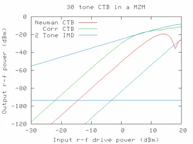
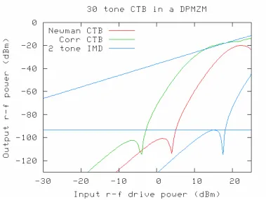
Figure 3 - 13: Time domain samples of a 30 tones in a Mach-Zender modulator ... 65
Figure 3 - 14: Power sweeps of 30 tones in a MZM. ... 66
Figure 3 - 15: 30 tone CTB in a linearized modulator. ... 67
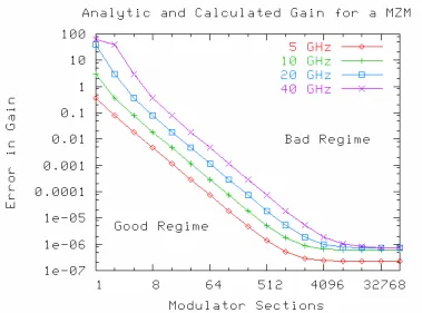
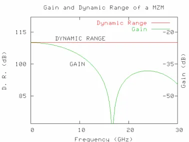
Figure 4 - 1: The convergence of the calculation of the gain of a simple MZM... 74
Figure 4 - 2: Gain and dynamic range of a standard Mach-Zehnder modulator ... 77
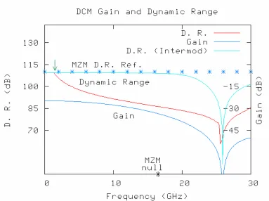
Figure 4 - 3: Gain and dynamic range of a simple directional coupler modulator... 78
Figure 4 - 4: Non-linearized Y-fed DCM gain and dynamic range... 79
Figure 4 - 5: Dynamic range comparison of four broadband linearized modulators... 80
Figure 4 - 6: Dynamic range comparison of four broadband linearized modulators... 81
Figure 4 - 7: Dynamic range comparison of two sub-octave linearized modulators... 85
Figure 4 - 8: Dynamic range comparison with 1 kHz signal bandwidth... 88
Figure 4 - 9: Dynamic range comparison with 1 kHz signal bandwidth... 89
Figure 4 - 10: Dynamic range comparison with 1 MHz signal bandwidth... 90
Figure 4 - 11: Dynamic range comparison with 1 MHz signal bandwidth... 91
Figure 4 - 12: Dynamic range comparison with 1 GHz signal bandwidth... 92
Figure 4 - 13: Re-optimization of the SoDCM by slightly adjusting the bias ... 93
Figure 4 - 15: The dynamic range of the SoDCM re-optimized ...95
Figure 4 - 16: Dynamic range versus frequency for the DCM. ... 96
Figure 4 - 17: Dynamic range versus frequency for the DCM2P... 98
Figure 4 - 18: Dynamic range of rephased YFDCM (θ=1.43π)... 99
Figure 4 - 19: Dynamic range of a rephrased CMZM... 100
Figure 4 - 20: Dynamic range of the SoDSMZM. ... 101
Figure 4 - 21: Dynamic range versus frequency for the SDCM ... 102
Figure 4 - 22: The gain of a standard MZM with multiple electrode segments. ... 103
Figure 4 - 23: The gain of a Y-fed DCM. ... 105
Figure 4 - 24: The transfer function of Y-fed DCMs... 106
Figure 4 - 25: The gain of a Y-fed DCM ... 108
Figure 4 - 26: The gain of DCM... 110
Figure 4 - 27: Gain of the DCM... 111
Figure 5 - 1: Phase modulator in reflective traveling wave configuration. ... 114
Figure 5 - 2: MZM and DCM reflection modulators ... 117
Figure 5 - 3: DSMZM reflection modulators... 118
Figure 5 - 4: The optimal optical split as a function of the RF split. ... 121
Figure 5 - 5: The optimal dynamic range ... 122
Figure 5 - 6: A DPMZ with a precise optical split. ... 123
Figure 5 - 7: The waveguide an electrode structure of a sensitivity split... 126
Figure 6 - 1 Actual electrode mask used in FTS-1 design... 129
Figure 6 - 2: D-c transfer function of Sheehy’s DCM... 130
Figure 6 - 3: (a) Curve fit to experimental data... 131
Figure 6 - 4: Oscilloscope Polaroid of the operation of directional coupler... 133
Figure 6 - 5: “Mouse-bite” defects (a) on LINC-1 directional coupler... 135
Figure 6 - 6: Electrode mask UVC-el-1... 136
Figure 6 - 7: Photograph of the modulator mounting structure. ... 139
Figure 6 - 8: Modulator chip mounted on the mechanical carrier stage ... 140
Figure 6 - 9: Blown up view of the modulator chip and millimeter-wave slab guide... 141
Figure 6 - 10: Slab dielectric waveguide coupling scheme for millimeter-wave modulators.... 142
Figure 6 - 11: Photograph of a “back-to-back” coupling structure. ... 143
Figure 6 - 12: Plot of dielectric constant correction factor... 144
Figure 6 - 13: a) A layer of Stycast between two polypropylene feeds... 146
Figure 6 - 14: A slab layer of Stycast 5 between two polypropylene feeds... 148
LIST OF TABLES
Number Page
3-1: Parameters of the canonical link defined for this study …….……….28
3-2: Gain, 1-Hz DR, 4-MHz DR, and noise figure ………...51
3-3: Parameter tolerance of standard and linearized modulators ………...59
C h a p t e r 1
INTRODUCTION
In the last few decades the field of optics has become very important. Especially with the invention of optical fiber, technologies for the manipulation and transport of coherent light offer great advantages in a wide range of applications. Optical systems are used to send information from as long a distance as across oceans, to as short a distance as the machine room or even the back-plane in an equipment chassis. There are commercial fiber-optic products in telecom voice & data, computer networking, cable TV, and scientific measurement. In the defense industry fiber-optic systems are used in similar applications, and in addition, they are used in antenna remoting and some advanced weaponry. Fiber-optics promises significant bandwidth, above a terahertz, and low transport loss, 0.1 dB/km, all in a “light” cable.
A basic fiber-optic data link consists of an electrical amplifier, a laser, a means of modulating the optical signal with the electrical signal, a length of fiber, an optical detector, and an electrical post-amplifier. The “intrinsic link” is the laser, modulator, fiber, and detector. Link engineers select a set of optical components that when combined form a fiber-optic link to optimally meet the system requirements. In component research and engineering, the aim is to improve the figures of merit of particular components of the fiber-optic link. In this thesis electrooptic modulators are evaluated in the context of a normalized intrinsic link. The application scope is 1-100 GHz analog links used for short range military applications, such as antenna remoting. However, many of the results apply to links more broadly in other applications.
possible for even an intrinsic link to have net positive power gain if sufficient optical laser power is used, as shown by Cox in Ref. [1.1]. The noise figure is the noise power out of the link divided by GkT0B (link gain, Boltzmann’s constant, room temperature taken as 290K, and noise bandwidth), usually expressed in dB. Dynamic range is the peak power ratio of the signal to the dominant distortion term, also usually expressed in dB. Bandwidth (sometimes termed “noise bandwidth”) is the electrical frequency range passed by the link. It often is not possible to simultaneously optimize all of the figures of merit, so trade-off analysis is employed to evaluate modulators for different link configurations.
There are two different approaches to optical modulation in the fiber-optic link, direct modulation of the laser and external modulation of the laser output. Many links employ direct modulation, in which the modulation voltage is applied to the power supply of the laser. While simple, direct modulation is undesirable in noise-sensitive applications because it creates chirp, phase modulation that can be converted to amplitude modulation distortion in the receiver. In high fidelity links, the modulation function is usually separated from the laser into an external component. There are three types of external modulators in common use today: electro-absorption modulators based on the semiconductors gallium arsenide or indium phosphide, electrooptic modulators based on polarized polymers, and electrooptic modulators based electrooptic crystals such as lithium niobate, and other materials. The theoretical calculations in this thesis apply to all forms of high fidelity modulators, while the laboratory work focuses on high frequency LiNbO3 electrooptic modulators.
Thesis Organization
Chapter 1 introduces the thesis topic.
Chapter 2 gives a brief tutorial overview of the different kinds of lithium niobate electrooptic modulators treated in this research. The Mach-Zehnder modulator (MZM) is by far the most common configuration used today, but the directional-coupler modulator (DCM) also offers some attractive characteristics. The linearity and frequency limitations of both these modulators are introduced.
Chapter 3 addresses distortion and its reduction in various electrooptic modulator configurations. This work follows the work done in Ref. [3.8] but adds additional modulators and additional comparisons. A consistent link model is defined against which to compare many different modulators and linearization schemes. Gain, noise figure, and dynamic range are defined and calculated numerically for all of the different modulators, as appropriate for a single analog signal. The modulators are further compared using composite triple beat and composite second-order distortion, the figure of merit for CATV, where multiple channels are transmitted over the link. Finally, the modulators are compared for their sensitivity to manufacturing and bias parameters.
Chapter 4 addresses the bandwidth limitations of different modulators and linearization schemes. A numerical modulator simulation computer program is defined. The program calculates the gain and dynamic range for the modulators defined in Chapter 2. The question of whether a linearization scheme can be reoptimized for a particular frequency within the band-pass for high frequency operation is answered. The effect of multiple electrode segments, “rephasing on the average,” on dynamic range is analyzed. Much of this work was published in Ref. [4.2], but there are some extensions to this work that appear originally here.
on the average” with a two segment electrode. The technique is broadly applicable to different modulators. It is covered in U.S. Patent 5,076,655. The second modulator improvement uses “sensitivity splits.” This technique applies to two well-known linearized modulators. It significantly reduces the complexity of the modulator design by building asymmetry into the modulator, and then taking advantage of the fact that the modulators only need one precisely controlled degree of freedom, whereas the published version of the prototype modulator structure calls out for two precisely controlled degrees of freedom.
Chapter 6 covers the laboratory work done on high-frequency antenna-coupled external modulators. A 100 GHz directional coupler modulator is demonstrated. This experiment follows on work done by Sheehy in Refs. [1.2] and [1.3]. A set of directional coupler modulators with different electrical lengths and different modulator electrode lengths (physical length) was fabricated and characterized. The r-f feed structure for antenna-coupled modulators was optimized. A successful demonstration of the basic operation of this device was made very early in the work, and further improvements were carried out. Unfortunately, this portion of the study had to be abandoned (due to events beyond our control) before the improved device could be fully demonstrated.
C h a p t e r 2
The Electrooptic Effect
Electrooptic modulators of the variety studied in this thesis exploit the Pockel's effect. In crystals such as LiNbO3, the index of refraction varies linearly with the applied electric field, with the constant of proportionality depending on the orientation of the electric field with respect to the crystallographic axes. The resulting change in the optical path length of the light passing through the crystal is proportional to the voltage applied to a set of electrodes. Over a fixed physical length of crystal, this converts to a phase shift of the light passing through it.
The effect of an applied electric field on the propagation of light is defined by the change of
the indices of refractionin the tensor equation∆(1/n2)=RE. ∆(1/n2) gives the change in the index of refraction for the elements of the tensor ∆, R is the tensor of electrooptic coefficients, and E is the vector of the applied electric field. (See, for example Ref. [2.1]). There are six relevant indices of refraction from the index ellipsoid, three terms for the three principle directions (x, y, and z), and three cross terms. An electric field has x, y, and z components, so in general this effect is described with a 6 x 3 tensor, R. Each component
∆(1/n2)
i for 1 < i < 6 is the dot product of the i-th row of R with the electric field vector. In non-electrooptic crystals (centrosymmetric), all of the terms rij are zero. Most electrooptic crystals have some degree of symmetry leading to many of the rij terms equaling zero. The electrooptic effect is generally very small, but the crystal lithium niobate (LiNbO3) possesses relatively large values of these electrooptic coefficients, and has other desirable properties (hardness, non-hydroscopic, etc.). As well, LiNbO3 is a “3m” symmetric crystal and has 8 non-zero terms, of which there are 4 distinct absolute values, some terms are equal, and some are equal and opposite. For optical wavelengths of interest in this study1 the electrooptic constants are (in picometers per volt):
• r13= r23 = 8.6 pm/V,
• r22 = -r12 = -r61 = 3.4 pm/V,
• r33 = 30.8 pm/V,
• r51 = r42 = 28 pm/V.
The crystals are cut and used in an orientation to maximize the field projected onto the direction with the largest electrooptic effect. Clearly, it would be inefficient to rely on the r13 and r22 terms in LiNbO3. While the formalism to describe the electrooptic effect is fairly complex, in practice there is only one scalar quantity used in the analysis of electrooptic modulators based on LiNbO3, that is r33 (30.8pm/V), which describes the effect of an applied electric field in the z-direction on an optical wave polarized in the z-direction. For z-cut LiNbO3 the z-axis is normal to the crystal and the optical wave is “TM” polarized and for the x-cut LiNbO3, the x-axis is normal to the crystal and the optical field is “TE” polarized.
Electrooptic Modulation in Bulk Crystals
not interfere with the optical beam. Even so, it takes a lot of voltage to make an appreciable phase shift using bulk crystals. The electrooptic induced change in electrical path length is given by Γ=(2πf/c)(Lm/d)no3rV in the transverse configuration, where Lm is the length of the crystal, d is the spacing between the electrodes, and r is the appropriate rij for the crystal orientation. The half-wave voltage, or Vπ, is the voltage at which the optical beam has experienced an additional 1800 phase shift. For a 1.3 µm beam in LiNbO
3 in which the r33 electrooptic coefficient used is about 4 kV assuming (ℓ/d) = 1. If the crystal is four times longer than it is high, then Vπ is 1 kV. The voltages are even higher for crystals with smaller values of electrooptic coefficients, such as ammonium dihydrogen phosphate (ADP) or potassium dihydrogen phosphate (KDP) or their deuterated analogs.
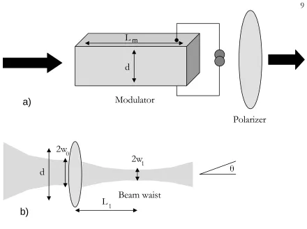
One might think that simply increasing (Lm/d) would solve the problem. This is not the case. As a practical matter, it becomes increasingly difficult to fabricate long, thin crystals. However, a more fundamental limitation occurs because of diffraction of the propagating light. If the transverse dimension d is made very small, the light propagating through the crystal will spread more rapidly, and hit the sides of the crystal, thus being absorbed. The optimum strategy for a light beam with a Gaussian transverse distribution is to place a Gaussian focus or beam waist half-way through the crystal, so that the propagation path is symmetrical. With this strategy, there is still an optimum (l/d). This is illustrated following the derivation for a Gaussian beam in a lens waveguide from Ref. [2.1]. Assuming in Figure 2 - 1b that the lens has a focal length ƒ, 2w0 is the beam waist diameter at the thin lens, 2w1 is the beam waist diameter at the minimum in the crystal, and θ is the beam diffraction angle of the far field, then
0 1 2 0 , , . 1 ( )
L
md
Modulator
a)
Polarizer
0
2w
1
2w
θ
d
Beam waist
L
1 [image:21.612.104.544.71.399.2]b)
Figure 2 - 1: a) Bulk crystal modulator in transverse configuration, b) Illustration of Gaussian beam waists in a bulk crystal modulator.
manufacturable crystal. This can be achieved with the introduction of waveguides in the crystal.
Waveguide Phase Modulators
The ability to fabricate optical waveguides in electrooptic crystals removes this limitation on (L/d). The waveguide eliminates diffraction, so that the crystal length may be made as long as required to achieve the desired sensitivity, limited only by optical loss in the crystal. And the transverse dimension d is no longer limited by the fragility of crystal fabrication; the bulk of the crystal mechanically supports the in situ wavelength-scale waveguide. This technique has reduced the Vπ by three orders of magnitude or more over the best bulk crystal modulators, making these devices suitable for a wide range of applications.
To make an optical waveguide, photolithography is used to define a strip mask on the crystal surface. In titanium in-diffused waveguides, a thin metal layer of a few hundred angstroms, by several micrometers in width, is deposited through the mask and then in-diffused into the crystal by a heating it at very high temperature, around 1050º C. The titanium atoms enter the crystal lattice slightly increasing the index of refraction in the crystal by about ∆n=0.01, as described in Ref. [2.3],2 creating a dielectric waveguide about 4 µm deep, centered about 2 µm below the crystal surface, and about 6 µm wide for single mode operation at an optical wavelength of 1310 nm. The electric field is applied perpendicular to the waveguide, exciting the transverse mode of modulation. The electrodes are also defined by photolithography; they are located on the surface of the crystal, and separated by the thickness of the waveguide. This reduces the required voltage to about 10 V for a half-wave phase shift over a modulator length of about 10mm. By increasing the length and optimizing the electrode geometry, researchers have reduced the required voltage to about 2 V in modern LiNbO3 modulators, yielding (ℓ/d) = 2000.
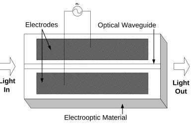
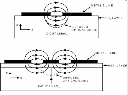
A phase modulator is the simplest modulator to build. Figure 2 - 2 shows a waveguide-based lithium niobate phase modulator in the “x-cut” orientation. There is a single optical waveguide parallel to the y-axis of the crystal. The electrodes are fabricated as strips of metal (usually gold) on top of the crystal. The gap between the waveguides is sized and positioned to maximize the electric field component along the direction of the crystal with the strongest electrooptic coefficient. In case of “x-cut” lithium niobate, light propagates along the y-direction, the z-direction is normal to the substrate, and the x-direction is along the surface, perpendicular to the direction of propagation. The electric field lines penetrate down into the crystal, continue perpendicular to the waveguide in the z-direction of the crystal, and then go back up to the opposite electrode. The fields are illustrated explicitly for both x-cut and z-cut modulators in Figure 2 - 3.
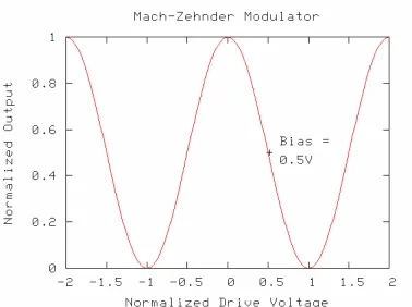
Intensity Modulators Based on Mach-Zehnder Interferometers
output is zero is termed “Vπ.” For analog applications, the modulator is typically d-c biased
at Vπ/2, so that the optical output is 50% with no modulation applied. Applying the modulation voltage in addition to this bias then results in intensity modulation about the most linear portion of the cosine-squared curve. That gives 3-db in optical loss from the modulator transfer function in addition to the mode-matching losses at the crystal interfaces and any propagation losses through the crystal. A useful property of simple interference modulators like the MZM, with a cosine-squared transfer function, is that when biased at the half-wave point, all even-order harmonics of the modulating signal are zero, since all even-order derivatives of the cosine-squared function are zero at that point. The distortion produced by the modulator is thus dominated by the odd-order intermodulation products and odd-order harmonics from the (non-zero) odd-order derivatives of the transfer function, which have
Light
Out
Light
In
Optical Waveguide
Electrooptic Material
Electrodes
[image:24.612.133.518.355.605.2]AC
Figure 2 - 3: Schematic cross-section view of a phase modulator in an x-cut lithium niobate crystal (top schematic) and a z-cut lithium niobate crystal (bottom schematic).
their maximum values at this bias point. The third-order intermodulation is the strongest of these and is usually the limiting distortion.
Light
Out
Light
In
Optical Waveguide
Electrooptic Material
Electrodes
[image:26.612.137.528.78.323.2]AC
Figure 2 - 4: Mach-Zehnder modulator based in indiffused waveguides in an electrooptic crystal.
Waveguide Electrooptic Modulators Based on Directional
Couplers
Figure 2 - 5: Mach-Zehnder Modulator transfer function: normalized output intensity as a function of drive voltage (normalized to Vπ).
energy from one guide to the other. The fields in the directional coupler are shown in Figure 2 - 7.
Light
Out
Light
In
Optical Waveguide
Electrooptic Material
Electrodes
AC
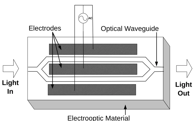
Figure 2 - 6: Directional Coupler Modulator based on indiffused waveguides in an electrooptic crystal. The z-direction of the crystal is used to create the modulation. Not shown in the figure, the waveguides are typically bent through anti-symmetric “S” curves between the edge of the crystal and the active area of the modulator to provide more lateral separation of the two guides for ease in coupling light in and out.
Figure 2 - 7: Fields in a directional coupler modulator looking down the waveguides; the top view is of the crystal and electrodes, the bottom view is of the overlap of the optical field intensity between the two waveguides.
The coupling is created by the same physical mechanism as in r-f and electronic directional couplers; and the governing equations are very similar. The fields of one waveguide partially penetrate the other, and there is a transfer of optical energy. In a modulator, the applied electrical field linearly changes the strength with which light couples from one guide to the next. In approximate form, this device creates a sin2(x)/x2 transfer function. Unlike the Mach-Zehnder, it does not have the property that all even-order distortion terms cancel at a single bias point, and it is not as robust to fabrication errors, particularly those affecting the optical coupling, such as the guide-to-guide spacing and the size of the “tails.” However, it can be employed in many configurations, the subject of future chapters of this thesis, which make it an interesting alternative to the straightforward Mach-Zehnder modulator.
Fidelity in Electrooptic Modulators
Figure 2 - 8: Transfer functions of both arms of a directional coupler modulator. The bias voltage is 0.43 VS.
Frequency and Bandwidth Limitations in Electrooptic
Modulators
Frequency response (and bandwidth in the case of baseband modulators) is a key issue for external electrooptic modulators. The modulators shown in Figure 2 - 4 and Figure 2 - 6 use lumped capacitance electrodes. Typically, an inductance L and a load resistor RL is placed in parallel with this capacitance to make an RLC circuit, with a 3-dB point given by ∆f=1/(2πRLCmod). Assuming the modulator has a 50 pF capacitance and the load resistance is 50 Ω, then the 3-dB point is 64 MHz away from the center frequency. This will have a bandwidth if f=2/(2πRLCmod), which is 128 MHz, but now centered at the desired operating frequency. Modern communication systems require bandwidths in the GHz range, so the lumped capacitance electrode structures simply are not practical. A different implementation is required.4
Even for applications where the bandwidth of a resonant circuit is sufficient, there is a fundamental limitation to the frequency of operation of an electrooptic modulator that comes from the finite transit time of the modulated beam. Essentially, the phase of the modulating voltage changes while the light is traversing the length of the crystal so that, effectively, the same voltage is not applied over the entire length. This results in a net reduction from the peak retardation of
1
i M dM d
e
r
i
− ω τ
−
=
ω τ
, (2.2)where τd from (2.2) is the transit time of light through the crystal, τd = nℓ/c, and ωM is the radial frequency of operation (see, for example Ref. [2.1]). The modulation amplitude reduction factor is a sinc function of ωMτd. Taking the absolute value of |r| = 0.9, gives a 3 For two signal components at f1 and f2, the third-order products are at 2f1-f2 and 2f2-f1, both only |f2-f1| away from a
signal component.
maximum frequency of c/(4nℓ), or equivalently 1/(4td). In LiNbO3, n=2.15, and for a 10 mm modulator, this is 3.49 GHz.
The solution to both the narrow bandwidth RC response of the electrode structure and the finite transit time of the optical beam is to use traveling wave electrodes. In a traveling wave configuration, the electrodes become a transmission line. The line is excited at the input end, the modulating electrical field propagates down the electrodes parallel to the propagation of the optical wave, and then is terminated in matching impedance at the end of the electrodes. The electrodes no longer form an RC filter; instead they become a transmission line with distributed inductance and capacitance. The issues of loss, reflections, and radiation must now be considered instead.
The finite transit time problem is improved but not totally solved by the transmission line electrodes because there is generally a different velocity between the optical and r-f waves. The reduction factor expression now becomes
(1 / )
1
.
(1
/ )
M d m o
i n n
M d m o
e
r
i
n
− ω τ −
−
=
ω τ
−
n
(2.3)Taking the optical velocity to be c/no and the microwave velocity to be c/nm, this gives an improvement of the frequency at which |r| = 0.9 of |1/(1- nm/no)| over the previous value c/4noℓ. When no = nm then the optical wave and the r-f wave are traveling with the same phase velocity and the there is no velocity mismatch. When nm = 0 (infinite microwave phase velocity) then the reduction factor is the same as the lumped electrode. For lithium niobate the r-f phase velocity is slower than the optical phase velocity for waves traveling in parallel. For example, in LiNbO3 for fields in the z-direction, ne = 2.15. For the microwave velocity, the electric permittivity is 28. However, half of the electric field between the electrodes is in the air so it is appropriate to use the average permittivity (recall Figure 2 - 3). The effective microwave index of refraction is taken as
1/ 2 1/ 2 1 .
2 r m m
n = ε = ⎜⎛ε + ⎞⎟
Here εr is the permittivity for the crystallographic axis of propagation. For propagation in a lithium niobate crystal in which the electric field is equally split between the z-axis and the x-axis, εr=( εxεz)1/2 = (28*43) 1/2 = 34.7. And thus nm= 4.2. In a lithium niobate traveling wave modulator where both fields travel in parallel and are polarized in the same direction, the frequency at which |r| = 0.9 is c/4nℓ(1-n/nm) = 7.15 GHz for a 10 mm modulation section, an improvement of more than 2x over the “lumped element” electrodes, but clearly still frequency limited.
Increasing Frequency Response of E-O Modulators by Velocity
Matching
Velocity-matching techniques are often used to improve the frequency response of the traveling wave modulator. In Ref. [2.3] many velocity matching techniques are described and referenced. In waveguide-based modulators the fields propagate down coplanar electrodes on the surface; some field lines penetrate into the crystal (these are useful for modulation) and other field lines are in the air. While Eqn. (2.4) assumes an equal split, it is possible to create thick enough electrodes so that more than half of the electric field is in air, resulting in nm = f(nair, nmb) = no. This is done by up-plating the coplanar waveguide. Unfortunately, this matching technique also decreases the modulator sensitivity to the electric field (increases Vπ) since the field drawn up into the air between the electrodes no longer passes through the optical waveguides. In addition to up-plating the electrodes, a thick SiO2 buffering layer can be deposited between the crystal and the electrodes. The microwave index of refraction of SiO2 is less than that of lithium niobate so the electric field that passes through the SiO2 layer also reduces the effective refractive index of the transmission line electrode structure. A number of successful high frequency modulator experiments have been made exploiting the velocity matching technique beyond 40 GHz, for example, velocity matching techniques were used to go above 30 GHz in Ref. [2.4] and truly exceptional work was done to get 100 GHz velocity matched modulators in ref. [2.5].
electrode loss becomes a serious compounding problem. In essence, the electrode loss will limit the “length” of the modulator no matter how long it is made physically. An alternative technique that addresses the velocity mismatch problem is called “velocity matching on the average” and has been demonstrated in several forms. See, for example Ref. [2.6]. A velocity-mismatched electrode may be divided into sections, where each section is typically made shorter than the maximum length of a useful modulating electrode at the target frequency, as determined by electrode loss and velocity mismatch. The modulating electric field is then arranged to be “re-phased” at the beginning of each modulator section, so that it never gets too far out of step with the modulated optical wave; it is “velocity matched on the average.”
One method of accomplishing this was the “phase reversal” modulator demonstrated by Alferness, et al [2.7] in which the electrode sections were made 180o long in phase (at some desired modulation frequency), then connected to the next electrode section with an electrical transposition, and so forth down the entire structure. This assured “phase matching on the average,” but only at one frequency, where the sections are 180º in phase delay. This is not true velocity matching or true-time-delay matching. The bandwidth of the modulator decreased as more sections were added.
Another technique was proposed and patented by Schaffner and Bridges, Ref. [2.8], in which the modulating signal is divided by a multi-branched transmission-line feed that has varying lengths that just compensate for the optical delay down the waveguide under the electrode structure. Each section of the modulator is then fed at its entrance end with the proper delay to equal the optical delay to that section. This is a true velocity matching scheme and has the advantage of not narrowing the bandwidth, but it does have the disadvantage of dividing the modulating signal by the number of paths, all of which have transmission loss.
operation by the bandwidth of the on-surface antennas and the wave radiating structure (but
Figure 2 - 9: Schematic of antenna-coupled phase modulator. The microwave signal is received by the antenna elements in synchronism with the arriving optical wave that travels through the waveguide. Selection of the appropriate angle of incidence of the microwave yields a velocity matched modulator “on the average,” discussed in Ref. [2.6].
C h a p t e r 3
DISTORTION IN MODULATION
Abstract
Link Model
Figure 3 - 1 shows a simple intensity modulated photonic link. The intrinsic link consists of a low noise laser, an electrooptic modulator, a length of fiber, and a square-law detector. Electronic pre- and post-amplifiers are almost always included in actual practice, but with the exception of their signal bandwidth parameter, they are left out of the calculation. Since there is modulator non-linearity, the performance calculation must be made numerically, and specific numerical values for the component parameters must also be used. It is desirable to establish a reference link with which to compare modulation schemes; the numerical parameters from Ref. [3.8] are used here to compare with the results of their work, and these parameters are given in Table 3-1. Note that these are “garden variety” values, not “best ever” results obtained only in research laboratories. In fact, they are likely not as good as in the latest commercial fiber-optic links (available in 2005), but they suffice for a comparison of linearized modulator performance from one modulator to another. This link is as simple as possible while still capturing the properties of the modulator. Non-linear effects in the fiber and the detector are ignored. While it would be appropriate to add such effects as Brouillin scattering, noise from optical amplification, and photodetector non-linearity to accurately model a link, these effects are unnecessary for the comparison of linearized modulation schemes and are left out.
These parameters normalize the input r-f drive, the output optical intensity and the noise level of the electrooptic modulator. Given this, and the d-c transfer function of each modulator, a standard Fourier analysis is applied to obtain gain, dynamic range, and noise figure for any electrooptic modulator. While some of these figures of merit are analytically calculable for some modulators (i.e., for the simple MZM, the cosine-squared function can be expanded in a Bessel series), it is more systematic to design a numerical calculation and use it for every modulator.
Figure 3 - 1: Canonical model of an optical link for evaluating external modulators.
Analysis with One and Two Tones
Table 3-1: Canonical Link Parameters
Parameter Symbol Value Units
Laser Power PL 100 mW
Laser Noise RIN -165 dBm/Hz
Modulator Sensitivity Vπ, VS 10 V
Modulator Impedance RM 50 Ω
Velocity Mismatch (nmicro-nopt) ∆n 1.8 -
Modulator Length ℓM 10 mm
Optical Loss LO -10 dB
Detector Responsivity ηD 0.7 A/W
Detector Load RD 50 Ω
Signal Bandwidth BW 1 or 106 Hz
Maximum Photocurrent PLL0 ηD 7 mA
modulator figures of merit. Note that the calculations ignore any deviation from ideal square law behavior of the photodetector, even though such deviations have been measured and are, in fact, important for links with high average currents on the photodetector, of example, see Ref [3.1]. For a clear comparison of the properties of low-distortion modulators, other components in the optical link are assumed to be ideal.
Small signal gain is determined from single tone analysis. Let P(pIN,t) be the electrical signal power after the detector, given the modulator r-f drive power pIN. Let P~(p
IN,f) be the Fourier transform of P(pIN,t). The gain is
10{ [ ( , )] ( )}.
dB Log pin f Log pin
Gain
= Ρ∼ − (3.1)The small signal gain is obtained by evaluating Eqn. (3.1) at sufficiently small pIN such that the log-log plot of P~(p
IN,f) is linear with slope one. In practice, we take pIN = -100 dBm to determine small-signal gain, which is about the geometric mean of pSAT (the power that drives the modulator voltage to about Vπ and the precision of double precision floating point numbers.5 The frequency of the tone is set to an integer multiple of 2π so that the gain and any harmonics will fall precisely on the discrete samples of the FFT, making the calculation fast and accurate. This frequency does not correspond to a physical frequency, and thus cannot be used to analyze the roll-off of the modulator until the finite transit time of the optical and electrical signals, and frequency-dependent r-f loss is introduced into the analysis (Chapter 4). The phase in a single-tone analysis has no effect in an intensity modulated link. Single-tone analysis also gives harmonic distortion levels.
Two-tone analysis captures the signal, harmonic distortion, and intermodulation distortion. By convention, the amplitudes of the two tones are set equal, which gives the worst case distortion. The frequencies are chosen to be consecutive integer multiples of 2π. It makes no difference if they are more largely spaced, provided they remain integer multiples of 2π. The input drive is represented functionally as
1
( ) 0.5
IN M(sin(2
) sin(2
)).
v t
=
P R
π
f t
+
π
f t
2−
) 0
(3.2)
The relative phase of the two tones makes no difference in the calculation. In the time-domain, the two tones form a harmonic oscillation at the mean frequency modulated by an envelope created by the beat of two signals. Changing the relative phase of the two signals only modifies the phase of the envelope oscillation relative to a universal reference frame; it does not change the shape of the time-domain signal, and consequently the relative phase of the tones has no effect on the dynamic range.
The spurious-free dynamic range, SFDRdB, is the power interval that spans the input power level at which the signal is just distinguishable from the link noise to the input power level at which the strongest distortion term becomes distinguishable from the noise. The calculation of SFDRdB is
~ ~
1 2 1
( ) 10 max{log[ ( ,2 )],log[ ( ,2 )]} ,
dB IN IN IN dB
D P = P P f − f P P f noise (3.3)
2
10log(
2
),
dB DC D DC D
noise
=
GkT
+
RIN I
⋅
R
+
eI
R
+
kT
(3.4)0
min(
IN|
DdB(PIN),
p
=
P
= (3.5)~
0 1
10 log[
( , )]
.
dB dB
SFDR
=
P
p
f
−
noise
(3.6)Of the roots of DdB(pIN), p0 is the root that occurs at the lowest power level, in the event that DdB(pIN) intersects the noise level at more than one value of pIN. SFDRdB is the difference between p0 and the input power level at which the signal intersects the noise level. Since the log-log plot of the signal has slope one, this interval is equivalent to the signal power [dB] minus the noise power [dB] at the r-f drive power at which the distortion power equals the noise level. Figure 3 - 2 shows the dynamic range calculation for a simple Mach-Zehnder modulator. In simple modulators, the log-log plots of the distortion terms are linear, intersecting the noise floor only once. In linearized modulators, the distortion terms may be nulled at some discrete power level or levels. Thus, they may cross the noise level more than once. It is then necessary to find all of the roots of RdB, the distortion minus the noise, and use the root representing the lowest RF drive power in the definition of dynamic range.
While dynamic range generally refers to all harmonics and intermodulation products, in non-linearized modulators, there are two dominant distortion terms, the second harmonic, P~(p
IN, 2f0), and the third-order intermodulation product, P~(pIN, 2f0-f1). This thesis distinguishes two categories of linearized modulators, defined by their operating bandwidths. If fUPPER and fLOWER are the upper and lower frequency edges of the operating band, then a sub-octave modulator has fUPPER < 2fLOWER and a super-octave modulator has fUPPER ≥ 2fLOWER. Dynamic range is treated differently for each case. Eqn. (3.3) applies to broadband, or super-octave modulators. That is, DdB(pIN) is the maximum of the second harmonic and the intermodulation product. In narrow band or sub-octave modulators, DdB(pIN) contains only the third-order intermodulation product, since the second harmonic falls outside the sub-octave bandwidth.
Signal and Intermod Power -180 -160 -140 -120 -100 -80 -60 -40 -20 0
-160 -140 -120 -100 -80 -60 -40 -20 0 20 40
Pin (dBm) Pou t ( d B m ) Signal Intermo Noise Floor Dynamic Range
-136 dB -26 dB
Dynamic Range
Figure 3 - 2: The signal (gain) and third-order intermodulation product of a link using a Mach-Zehnder modulator (MZM) and the parameters given in Table 3-1. Since there is no second harmonic distortion
in a normally biased MZM, DdB equals the
-approximating a true delta function in the limit of large N. And for any N, this gives the maximum signal excursion for a given input power level, making it the worst case for distortion. A correlated but non-equal set of phases yields the best case, the Newman condition. The most common relationship is an uncorrelated normal distribution of phases, which yields very good results statistically. The multi-tone case will be discussed in more detail in the section on Multi-Tone Analysis at the end of this chapter.
Linearized Modulators
Many linearization schemes have been proposed in the literature, most of which consist of some combination of MZMs or DCMs and may bias the modulators away from the half-wave levels. In fact, there are so many different variations that it has prompted one researcher, G. Betts, to make a “Darwin Chart,” from Ref. [3.2] reprinted here as Figure 3 - 3 with modifications. The chart depicts the evolution of various linearization schemes from their early ancestors, the simple MZM and DCM. The calculations prepared for this thesis cover 24 different modulator transfer functions, although only six key modulators (seven including an unrealizable “reference” modulator) are analyzed in-depth in this chapter.
Super Octave Modulators
A superoctave modulator is any modulator in which the passband is more than an octave wide (i.e., as defined above, the upper cutoff frequency is more than two times the lower cutoff frequency). This analysis addresses five broadband linearized modulators:
1. An ideal limiter, which is not physically realizable (LMTR),
2. Two Mach-Zehnder modulators in parallel optically (DPMZ),
3. Two Mach-Zehnder modulators in cascade optically (CMZM),
4. A directional coupler modulator with two passive bias sections in cascade (DCM2P),
Directional Coupler Mach-Zehnder Interferometer
Based Approaches Based Approaches
Figure 3 - 3: a “Darwin chart” of many proposed linearized modulators, reprinted from reference [Betts] and revised. Standard modulators MZM and DCM, sub-octave modulators SDSMZ and SDCM, and broadband modulators CMZM, YFDCM, DPMZ, and DCM2P. Note the DSMZ is shown with an r-f split, it doesn’t need one for linearization, however using one results in a lower shot noise link.
Current approach (SFDR = 110 dB/Hz)
RF applied to two electrodes RF applied to two electrodes
Kurazono, 1972 Kaminow, 1975
BIAS BIAS
Betts, 1996
BIAS 1:S BIAS
BIAS
Bridges and Schaffner, 1995
MZM
2nd-Order DCM
Lineariz i n ato Only
3rd-Order a Lineariz t n io
Only (Sub-octave)
2nd- and 3rd- Order Linearization (Broadband)
Farwell et al., 1991 Korotky and DeRidder, 1990
1:P BIAS 1:S BIAS 1:P RF
Skeie and Johnson, 1991
BIAS BIAS 1:S 1:P 1:S RF RF RF RF RF SoDCM SoDSMZM CMZM
Figure 3 - 4 shows the d-c transfer function for these five super-octave linearized modulators. The input voltage is normalized to Vπ or VS as appropriate.
Figure 3 - 4: Five superoctave modulators: The ideal limiter LMTR; the directional coupler with two passive sections DCM2P; the dual parallel Mach-Zehnder DPMZM, the cascade Mach-Zehnder CMZM, and the Y-Fed directional coupler YFDCM. Slopes may be either positive or negative about zero with no affect on linearity.
The Ideal Limiter
distortion. In sub-carrier multiplexing, clipping is a major concern since the phases of the many carriers may randomly align and drive the modulator into its clipping regime (for real modulators this is an approximation).
The normalized d-c transfer function (switching voltage and optical output both normalized to unity, with zero bias voltage at the operating point) for an ideal limiter is
1
min(max(0, n),1).
H = −
2 V (3.7)
The Dual Parallel Mach-Zehnder Modulator
The DPMZ is described in Refs. [3.3] and [3.4] and shown schematically in Figure 3 - 3. The optical and electrical input signals are split unequally between two Mach-Zehnder modulators, the output optical powers are combined incoherently in two photodetectors, and the electrical signals from the photodetectors are added. Both of the MZMs remain biased at their half-wave voltage, thus no even-order harmonic distortion is generated in either modulator. The relative r-f and optical levels are chosen such that the third-order intermodulation distortion from each modulator is exactly the same, but the desired signals are different. The relative phases of the modulation signals are chosen so that the IMD products exactly cancel. While the signals do subtract, they do not completely cancel. For example the bias points on the cosine-squared transfer function are chosen to have opposite slopes. The signal level from this modulator may be a couple of dB below that of a single MZM, but the dynamic range is greatly improved. For example, one modulator has a large portion of the optical power, a small portion of the r-f power, and is biased at 0.5 Vπ. The other modulator has the remainder of the r-f and optical power, and is biased at -0.5 Vπ.
The normalized d-c transfer function of a Dual Parallel Mach-Zehnder modulator (DPMZ) is
2 2
sin (
(
0.5)) (1
)sin ( 1
(
0.5)).
H
=
P
S V
−
+ −
P
−
S V
+
(3.8)zero (no cancellation) or too close to 0.5 (where signals would cancel along with the intermodulation distortion). The optimal points form a line segment in {S, P}, as will be discussed in Chapter 5.
This modulator has many alternative implementations in addition to the one shown in Figure 3 - 3. First, the link may have two separate fibers, in which case, the photodetector currents are summed as shown in the figure. Second, a 900 optical polarization rotator, may be inserted after one of the MZMs, putting the signals in polarization quadrature. The two signals are then combined in a single fiber, and detected in a single photodetector. Third, the two modulators can be driven by independent lasers at two slightly different wavelengths, and their outputs combined in a single fiber and detected by a single photodetector. The alternate implementations are chosen to reduce complexity and cost, but result in some performance compromises. For example, the polarization rotation scheme suffers from polarization cross talk in the fiber. It is interesting to note that the first experimental demonstration of a “Dual MZM” was made by Johnson at MIT Lincoln Laboratories (Ref. [3.3]), using only one MZM, but propagating both TE and TM optical modes. The sensitivity of TM and TE waves to the modulation voltage in lithium niobate is about 1:0.33, which is not the optimum of (0.1267)0.5 = 0.356, but is pretty close. The optical splitting ration was provided by rotation of the input polarization plane. Since the TE and TM waves are orthogonally polarized, they add incoherently on a single photodetector.
The Cascade Mach-Zehnder Modulator
properties developed in Ref. [3.5] defines the modulator with two ideal “combiners,” one after each MZM. The transfer function for the DSMZ is
( ) ( ) ( ) ( ),
t c p c p
M =M γ ×M x ×M γ ×M kx (3.9)
cos sin ( ) , sin cos j Mc j
ζ − ζ
⎛
ζ = ⎜− ζ ζ
⎝ ⎠ ⎞ ⎟ ⎟ (3.10) 0 ( ) . 0 jx p jx e M x e− ⎛ ⎞ = ⎜
⎝ ⎠ (3.11)
In Eqns. (3.9) - (3.11), ζ is the coupling parameter in the idea coupler and x and kx are the phase shifts in the MZM arms. The r-f power split is represented by the k parameter, and the modulation signal is applied to both phase shifters. The coupling parameter ζ is controlled by a bias voltage. Skeie gives the results of k=-0.5 and ζ = 27 degrees. These results were verified in our calculations.
⎛ ⎞ ⎜ ⎟ ⎝ ⎠
The Directional Coupler with Two Passive Biases
A DCM followed by two unmodulated but dc-biased electrode sections on the same underlying directional coupler makes a broadband linearized modulator (DCM2P), described by Farwell in Ref. [3.6], and shown schematically in Figure 3 - 3. The electrode sections have electrical lengths {0.5π, 0.25π, 0.25π}, where the last two sections of length 0.25π have an electrical bias but no r-f drive. The two passive sections with different bias voltages linearize the directional coupler modulator. The lengths are not unique, but were chosen to be able to analyze a specific example. The first and principal directional coupler modulator section is fed with the full optical input to one arm only and biased where its 2nd harmonic is nulled, no different from an ordinary directional coupler modulator. The outputs from the two arms of this DCM section are complementary. The two passive sections create a relative power split and phase shift between these two modulated signals. As the two signals are coupled together through the passive sections, the third-order intermodulation product is nulled, but only with the correct power split and relative phase shift, introduced by the two passive sections. This requires two degrees of freedom and hence there are two passive sections.7
The optical amplitude of a “simple” directional coupler modulator is given by
11 12 1
*
12 11 2
( , N) ( , N) IN m jm a ,
B V A V A
jm m a
θ = θ × = ⎜⎛ − ⎞⎟
−
⎝ ⎠ (3.12)
2
11 2
3
cos( 1 3 ) sin( 1 3 ), 1 3
N N
N
V
m V j
V
= θ + + θ +
+
2 N
V (3.13)
2
12 2
1
sin( 1 3 ). 1 3 N N m
V
= θ +
+ V
(3.14)
6 In Ref. [3.5] the difference between an ideal coupler and a DCM is not addressed. As a double check of the need to keep the phases aligned, we ran the optimization routines on the DSMZ with one DCM electrode after each modulator phase shifter, and we were unable to obtain a linearized modulator.
B(θ,VN) is a 2x1 vector of complex amplitudes corresponding to the outputs of the two waveguides in a directional coupler. The parameter m11 is the “through arm,” that is, the amplitude of the optical wave that exits the same waveguide that it entered, and m12 is the “cross term,” that is, the amplitude of the optical wave that couples to the opposite waveguide from the one it entered. The modulation voltage is normalized to the switching voltage VS by VN=V/VS. The electrical length θ is equal the coupling coefficient of the modulator times the physical length κℓ. A(θ,VN) is a unitary matrix; upon close inspection it is clear that the magnitude squared of the through-arm plus the magnitude squared of the cross term equals one for either input. The transfer function for a DCM is given by
2 1 11 1 12 2
2 *
2 11 2 12 1 , .
h m a jm a
h m a jm a
= ⋅ − ⋅
= ⋅ − ⋅ (3.15)
The transfer function for a DCM2P is given by
(
)
(
)
2
1 3 3 2 2 1 3
2
2 3 3 2 2 1 3
1 0 ( , ) ( , ) ( , ) ,
0 1 ( , ) ( , ) ( , ) .
b b RF b
b b RF b
h A v A v A v v
h A v A v A v v
θ θ θ
θ θ θ
= × × × + × = × × × + × IN IN A A (3.16)
The reference bias values for a DCM2P in normalized voltage for Eqn. (3.16) is {0.50529, 0.73803, 0.77000}, which is the normalized bias voltage for the r-f, and 2nd and 3rd passive bias section, as in Ref. [3.8]. This modulator has the advantage of no r-f split and no optical split. Furthermore, the only precise control needed is the bias voltage of the three directional coupler sections. Bias voltages are the easiest modulator parameter to fine tune. However, as will be shown Chapter 4, it is unusually difficult to preserve this linearization in the presence of velocity mismatch.
The Y-fed Directional Coupler
transfer function to be anti-symmetric. Similar to the MZM (and different from the DCM), all even-order harmonics are zero at the operating point, V=0. He proposed an electrical length of 0.707π, which is an innovative implementation of a 1x2 switch in that allows a complete transfer of optical power, and does not require any bias as would be required in a MZM or DCM. However, to use this structure as a linear modulator the electrical length should be π/2.
There are many variations of this modulator created by changing the electrical length, adding a passive (and unbiased) section and changing the electrode topology. As a matter of convention in this thesis, “standard YFDCM” is used to describe the Y-fed DCM with arbitrary electrical length, that may or may not be linearized. YFDCM is taken to be a specific version of the linearized modulator based on Thaniyavarn’s topology but with electrical length 1.43π. There are other ways of linearizing the standard YFDCM. First, it was found by Pucel, Ref. [3.10], that making the modulator a specific electrical length LA, followed by an additional passive coupling length LP (that is, without the modulation applied, and no bias) would cause the cubic distortion term to null, without upsetting the null of the second harmonic (after all, this is still an anti-symmetric device). Pucel gives the linearized values as LA=0.6π (active length) and LP=0.6121π (passive length). Second, in Ref. [3.11] Tavlykaev and Ramaswamy found that taking the YFDCM (as proposed by Thaniyavarn) and breaking the electrode and reversing the phase on the second section also creates a linearized modulator. In other words a modulation voltage V is applied over LA and –V is applied over LB. They give values of LA = 2.05π and LB = 0.5025π. They also demonstrate this modulator experimentally in Ref. [3.12].8 Third, in Ref. [3.13] it is shown that the standard YFDCM is linearized by simply increasing the electrical length of the modulated coupler to 1.4297π. In the author’s analysis program, it is shown that for both the standard DCM and the standard YFDCM, there is always a range of voltages as a function of electrical length, in which the third-order intermodulation distortion is nulled without a corresponding signal null. In the standard DCM this voltage can never be
zero for any electrical length, as there is no signal gain at that point. However, for the standard YFDCM, this voltage is zero at the electrical length 1.4297π. This is the only linearized YFDCM treated in detail in this thesis.
The d-c transfer function of the YFDCM is found from Eqn. (3.15) taking one-half of the through-arm amplitude and one half of the cross-term amplitude of the DCM Eqn. (3.12), that is the terms a1 and a2 of vector AIN are each equal to ½
(
)
2
2
3 1 1
cos( 1 3 ) sin 1 3 ,
2 2 1 3
n n n V j A V V −
= θ + + × θ +
+
2 n
V (3.17)
(
)
2 2
2 3 1
sin 1 3 .
2 1 3 n
n n
V
H A V
V
= = − θ +
+
2 (3.18)
The YFDCM is particularly sensitive to the optical phase in the Y-splitter. An optical phase shift of 1800 in the input to the two arms completely cancels the signal and produces only second harmonic. To keep the second harmonic below the third-order intermodulation requires a phase error of less than one optical degree depending on the operating signal bandwidth, Ref. [3.13].
It is also helpful to represent the transfer functions in terms of the physical directional coupler parameters; length ℓ, electrically induced coupling δ, coupling coefficient κ, see Ref. [3.14]:
(
)
2 2 1 sin . 2H = − 2δκ l δ + κ2
δ + κ
2 (3.19)
Sub-Octave Modulators
V
extra harmonic distortion is out of band, it does not interfere with the signal. Sub-octave modulators are inherently simpler devices than super-octave modulators, since they need only null one type of distortion. Both a Mach-Zehnder and a directional coupler based sub-octave modulator can be made with one precision parameter (bias voltage) and no r-f split.
The Sub-octave Dual Series Mach-Zehnder Modulator
The Sub-octave modulator, the Dual Series Mach-Zehnder (SoDSMZ) is described by Betts in Refs. [3.15] and [3.16]. It consists of two simple MZMs in series optically, but in parallel electrically. There is no required r-f split between the two modulators, and they both have the same bias.9 One monolithic electrode structure may cover two Mach-Zehnder optical interferometers. Thus its fabrication is as simple as modifying the waveguide design from a standard Mach-Zehnder by placing a Y-junction combiner followed by a splitter in the center of the modulator. The gain is reduced from a normal Mach-Zehnder by the fact that the modulator is effectively half as long (accommodating two modulators in series) and from the residual signal cancellation that is a necessary byproduct of the intermodulation cancellation.
The d-c transfer function for this modulator is
4
cos ( ).
H
=
(3.20)A normalized bias voltage of Vb = 0.581 nulls the third-order intermodulation distortion (V=Vb+Vrf).
The Sub-octave Directional Coupler Modulator
The Sub-octave Directional Coupler (SoDCM)