12090 South Memorial Parkway Huntsville, Alabama 35803-3308, USA (256) 880-0444 w (800) 322-3616 w Fax: (256) 882-0859
VMIVME-4905
Digital-to-Synchro/Resolver Converter
Board
Product Manual
© Copyright 2002. The information in this document has been carefully checked and is believed to be entirely reliable. While all reasonable efforts to ensure accuracy have been taken in the preparation of this manual, VMIC assumes no responsibility resulting from omissions or errors in this manual, or from the use of information contained herein.
VMIC reserves the right to make any changes, without notice, to this or any of VMIC’s products to improve reliability, performance, function, or design.
VMIC does not assume any liability arising out of the application or use of any product or circuit described herein; nor does VMIC convey any license under its patent rights or the rights of others.
For warranty and repair policies, refer to VMIC’s Standard Conditions of Sale.
AMXbus, BITMODULE, COSMODULE, DMAbus, IOMax
,
IOWorks Foundation, IOWorks Manager, IOWorks Server, MAGICWARE, MEGAMODULE, PLC ACCELERATOR (ACCELERATION), Quick Link, RTnet, Soft Logic Link, SRTbus, TESTCAL, “The Next Generation PLC”, The PLC Connection, TURBOMODULE, UCLIO, UIOD, UPLC, Visual Soft Logic Control(ler), VMEaccess, VMEbus Access, VMEmanager, VMEmonitor, VMEnet, VMEnet II, and VMEprobe are trademarks and The I/O Experts, The I/O Systems Experts, The Soft Logic Experts, and The Total Solutions Provider are service marks of VMIC.COPYRIGHT AND TRADEMARKS
VMIC
All Rights Reserved
This document shall not be duplicated, nor its contents used for any purpose, unless granted express written permission from VMIC.
The I/O man figure, IOWorks, IOWorks man figure, UIOC, Visual IOWorks and the VMIC logo are registered trademarks of VMIC.
ActiveX, Microsoft, Microsoft Access, MS-DOS, Visual Basic, Visual C++, Win32, Windows, Windows NT, and XENIX are registered trademarks of Microsoft Corporation.
MMX is trademarked, Celeron, Intel and Pentium are registered trademarks of Intel Corporation. PICMG and CompactPCI are registered trademarks of PCI Industrial Computer Manufacturers’ Group. Other registered trademarks are the property of their respective owners.
Table of Contents
List of Figures . . . 7
List of Tables . . . 9
Overview . . . 11
Functional Description . . . 12
Reference Material List. . . 13
Safety Summary . . . 14
Ground the System . . . 14
Do Not Operate in an Explosive Atmosphere . . . 14
Keep Away from Live Circuits . . . 14
Do Not Service or Adjust Alone . . . 14
Do Not Substitute Parts or Modify System. . . 14
Dangerous Procedure Warnings . . . 14
Safety Symbols Used in This Manual . . . 15
Chapter 1 - Theory of Operation . . . 17
Functional Operation . . . 17
Address Decode Logic . . . 19
VMEbus Foundation Logic . . . 20
Output Data and Control Registers . . . 21
Digital-to-Synchro/Resolver Modules . . . 22
Built-in-Test Hardware Operation . . . 23
Output Relay Control . . . 28
Power Connections . . . 29
5-Volt/Ampere Drive Option . . . 30
VMIVME-4905 Digital-to-Synchro Resolver Converter Board
6
Chapter 2 - Configuration and Installation . . . .33
Unpacking Procedures . . . 34
Connector and Jumper/Configuration . . . 35
Built-in-Test Output Configuration . . . 41
Hardware Connection to Synchro or Resolver . . . 42
Built-in-Test Configuration with Synchro/Resolver Test Bus . . . 43
Address Modifiers . . . 44
Address Selection Switches . . . 45
Calibration of High Drive Capability Boards . . . 46
Channel Zero . . . 46
Channel One . . . 46
Chapter 3 - Programming . . . .49
Built-in-Test Configuration with Synchro/Resolver Test Bus . . . 52
Built-in-Test Output Configuration. . . 52
Maintenance . . . 53
Maintenance . . . 53
List of Figures
Figure 1 Synchro/Resolver Test Subsystem (On-Line and Off-Line Testing) ... 12
Figure 1-1 VMIVME-4905 Digital-to-Synchro/Resolver Functional Block Diagram ... 18
Figure 1-2 Address Compare Functional Block Diagram ... 19
Figure 1-3 VMEbus Foundation Logic Block Diagram ... 20
Figure 1-4 Output Data and Control Registers Block Diagram ... 21
Figure 1-5 Digital-to-Synchro/Resolver Block Diagram ... 22
Figure 1-6 Built-in-Test Subsystem Configuration ... 24
Figure 1-7 Expanded Synchro/Resolver Subsystem with Built-in-Test ... 25
Figure 1-8 Quad Channel DSC/DRC Board VMIVME-4911 Functional Block Diagram ... 26
Figure 1-9 VMIVME-4910 Functional Block Diagram ... 27
Figure 1-10 Synchro/Resolver Output Functional Block Diagram ... 28
Figure 1-11 Power Connection Block Diagram ... 29
Figure 2-1 Switch and Jumper Locations ... 39
VMIVME-4905 Digital-to-Synchro/Resolver Converter Board
List of Tables
Table 2-1 P2, P3 Pinout . . . 36
Table 2-2 Jumper Factory Configuration . . . 37
Table 2-3 Jumper Configuration . . . 38
Table 2-4 Installation Table of Reference Voltage. . . 40
Table 2-5 Relay Functions**. . . 41
Table 3-1 Data Input Word: Bit Weights . . . 50
Table 3-2 Address Map and Register Bit Formats. . . 51
VMIVME-4905 Digital-to-Synchro/Resolver Converter Board
Overview
Introduction
The VMIVME-4905 board is a VMEbus compatible Digital-to-Synchro/ Resolver Converter (DSC/DRC) Board that utilizes either one or two
digital-to-synchro/resolver converters, depending upon the option chosen. The primary features are:
• Synchro or resolver outputs • .024 or 5.0 VA options
• 2.0 VA with output transformer option • One or two DSC/DRCs
• 14-bit converter with an accuracy as high as ±1 ARC minute (±4 ARC minute is standard)
• 8- or 16-bit VMEbus data transfers • Front panel Fail LED
• 115 Vrms or 26 Vrms reference excitation voltage* • Built-in-test features
• Supports off-line and on-line fault detection and isolation • Compatible with Intelligent I/O Controllers (IIOCs)
VMIVME-4905 Digital-to-Synchro/Resolver Converter Board
12
Functional Description
The DSC/DRC board is based on the NATEL HSDR 2514 converter module. The board supports a wide variety of options which are supported by configuring jumpers on the basic printed circuit board and by the installation of optional components. The options are listed in the Product Specification. The 4905 Board, with supporting Built-in-Test hardware, features both off-line and on-line fault detection and isolation. The Built-in-Test features require a VMIC Quad-Channel Synchro-to-Digital
Converter (SDC) Board (VMIVME-4911) or a single-channel SDC Board
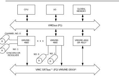
(VMIVME-4910) and a standard synchro test backplane (SRTbus™) installed in the P2 position of a standard VMEbus chassis, as shown in Figure 1 below. The board accepts a 14-bit digital input word (shaft angle) and a reference excitation voltage, and produces a synchro or resolver output.
The DSC/DRC board is provided with several options and is capable of interfacing with most standard synchro or resolver devices. The board is ideally suited for computer-based systems in which digital information is processed, such as
simulators, robotics, and other control-oriented systems. This product requires forced air cooling for the 5 volt amp (VA) option, and the 2.0 VA option with output isolation transformers.
NOTE: If this board is used with VMIC's intelligent I/O controller (IIOC) (VMIVME-9016), a quad-channel SDC board (VMIVME-4911) and a SRTbus™ is required for built-in-test. the IIOC firmware is not compatible with the
[image:12.612.123.520.405.664.2]VMIVME-4910.
Figure 1 Synchro/Resolver Test Subsystem (On-Line and Off-Line Testing)
CPU I/O GLOBAL
MEMORY
VMIVME- 4905
VMIVME- 4905
VMIVME-4910 OR 4911*
VMEbus (P1)
CHANNEL NO. 0
NO. 1 SYNCHRO OR
RESOLVER NO. 0 NO. 1
VMIC SRTbus™ (P2) VMIVME-SRXX*
Overview
Reference Material List
For a detailed description of the VMEbus, refer to The VMEbus Specification and
Handbook available from:
VMEbus International Trade Association (VITA) 7825 Gelding Dr. Suite No. 104
Scottsdale, AZ 85620-3415 (602) 951-8866
Fax: (602) 951-0720 e-mail: [email protected] Internet: www.vita.com
For detailed technical information concerning synchro/resolver theory, refer to the following source.
Synchro Conversion Handbook ILC Data Device Corporation 105 Wilbur Place
Bohemia, New York 11716
The following application and configuration guides are available from VMIC to assist the user in the selection, specification, and implementation of systems based on VMIC’s products.
Physical Description and Specifications, refer to Product Specification, 800-004905-000 available from:
VMIC
12090 South Memorial Pkwy. Huntsville, AL 35803-3308, USA (256) 880-0444
(800) 322-3616 FAX: (256) 882-0859 www.vmic.com
Title Document No.
Digital-to-Synchro/Resolver Converter Board Instruction Manual 500-004905-000 Synchro/Resolver-to-Digital Input Board with Built-in-Test
Instruction Manual 500-004911-000
Digital-to-Synchro/Resolver Converter Output Board Instruction Manual
500-004900-000
Synchro/Resolver (Built-in-Test) Subsystem Configuration Guide 825-000000-004 Digital Input Board Application Guide 825-000000-000
Title Document No.
VMIVME-4905 Digital-to-Synchro/Resolver Converter Board
14
Safety Summary
The following general safety precautions must be observed during all phases of the operation, service, and repair of this product. Failure to comply with these
precautions or with specific warnings elsewhere in this manual violates safety standards of design, manufacture, and intended use of this product.
VMIC assumes no liability for the customer’s failure to comply with these requirements.
Ground the System
To minimize shock hazard, the chassis and system cabinet must be connected to an electrical ground. A three-conductor AC power cable should be used. The power cable must either be plugged into an approved three-contact electrical outlet or used with a three-contact to two-contact adapter with the grounding wire (green) firmly connected to an electrical ground (safety ground) at the power outlet.
Do Not Operate in an Explosive Atmosphere
Do not operate the system in the presence of flammable gases or fumes. Operation of any electrical system in such an environment constitutes a definite safety hazard.
Keep Away from Live Circuits
Operating personnel must not remove product covers. Component replacement and internal adjustments must be made by qualified maintenance personnel. Do not replace components with power cable connected. Under certain conditions,
dangerous voltages may exist even with the power cable removed. To avoid injuries, always disconnect power and discharge circuits before touching them.
Do Not Service or Adjust Alone
Do not attempt internal service or adjustment unless another person, capable of rendering first aid and resuscitation, is present.
Do Not Substitute Parts or Modify System
Because of the danger of introducing additional hazards, do not install substitute parts or perform any unauthorized modification to the product. Return the product to VMIC for service and repair to ensure that safety features are maintained.
Dangerous Procedure Warnings
Warnings, such as the example below, precede only potentially dangerous procedures throughout this manual. Instructions contained in the warnings must be followed.
Overview
Safety Symbols Used in This Manual
STOP:
This
symbol informs the operator the that a practice or procedure should not be performed.Actions could result in injury or death to personnel, or could result in damage to or destruction of part or all of the system.WARNING: This sign denotes a hazard. It calls attention to a procedure, a practice, a condition, which, if not correctly performed or adhered to, could result in injury or death to personnel.
CAUTION: This sign denotes a hazard. It calls attention to an operating procedure, a practice, or a condition, which, if not correctly performed or adhered to, could result in damage to or destruction of part or all of the system.
VMIVME-4905 Digital-to-Synchro/Resolver Converter Board
CHAPTER
Theory of Operation
Contents
Address Decode Logic. . . 19
VMEbus Foundation Logic. . . 20
Output Data and Control Registers. . . 21
Digital-to-Synchro/Resolver Modules . . . 22
Built-in-Test Hardware Operation. . . 23
Output Relay Control . . . 28
Power Connections . . . 29
5-Volt/Ampere Drive Option. . . 32
2-Volt/Ampere Output Isolation Transformer Option. . . 33
Introduction
This section of the manual presents detailed information about the VMIVME-4905 Digital-to-Synchro/Resolver Converter (DSC/DRC) Board hardware operation. Information concerning programming is provided in Chapter 3.
Functional Operation
The VMIVME-4905 board design may be functionally divided into seven primary sections, as shown in the functional block diagram in Figure 1-1 on page 18. These primary functional sections are as follows:
• Address compare and control logic • VMEbus data transceivers
• Output data and control registers • Digital-to-synchro/resolver modules • Built-in-test bus
• Relay control • Power connections
18
1
VMIVME-4905 D igi tal -to -Sy nc h ro/R es ol ve r Conv er ter Bo ard Figure 1-1 VM IVME -490 5 D igita l-to -Syn ch ro/R e s ol ve r Fu nct ion al Bloc k D iag ram JUMPER SELECTABLE POWER AND REFERENCE INPUT OPTIONS FRONT PANEL CONNECTOR P3 +15 VDC -15 VDC RH RL +15 VDC -15 VDC RH RL +15 VDC -15 VDC RH RL CONTROL LOGIC DATA TRANS- CEIVERS 16 DATA ADDRESS COMPARE AND CONTROL ADDRESS SWITCHES OUT REG 0 DATA 14 DS OR DR MODULE TEST BUS CSR OUT REG 1 DSC OR DRC MODULE 14 K4 K3 K1 FRONT PANEL CONNECTOR P3 K2 CSR GND DIG GND DIG GND +5 VDC +5 VDC3 OR 4
3 OR 4
3 OR 4 3 OR 4
[image:18.612.80.711.70.493.2]Address Decode Logic
1
Address Decode Logic
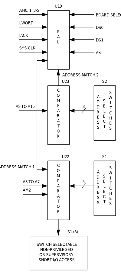
[image:19.612.224.424.233.683.2]A functional block diagram of the address decode logic is shown in Figure 1-2 below. Two eight-position "DIP" switches are provided to enable the user to select from a wide range of short I/O memory addresses for the board address. The user may also select nonprivileged or supervisory short I/O transfers. The board is configured at the factory to respond to short supervisory I/O transfers.
Figure 1-2 Address Compare Functional Block Diagram
P A L AM0, 1, 3-5
LWORD IACK BOARD SELECT C O M P A R A T O R A8 TO A15
S E L E C T A D D R E S S 8 S2 U23 C O M P A R A T O R
A3 TO A7 5
S1 U22 S W I T C H E S S E L E C T A D D R E S S S W I T C H E S U19 AM2 S1 (8) SWITCH SELECTABLE NON-PRIVILEGED OR SUPERVISORY SHORT I/O ACCESS SYS CLK
DS0
DS1
AS
ADDRESS MATCH 2
20
1
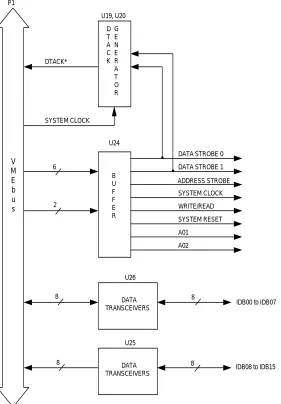
VMIVME-4905 Digital-to-Synchro/Resolver Converter BoardVMEbus Foundation Logic
[image:20.612.151.432.262.666.2]The DSC/DRC Board VMEbus foundation logic, shown in Figure 1-3 below, consists primarily of a DTACK generator, control signal buffers, and data transceivers. These transceivers buffer data to be transmitted to the output registers and to the Control and Status Register (CSR), which controls the front panel Fail LED and output isolation switches. The control logic is designed to support 8- and 16-bit transfers. Address bits A01 and A02 are decoded to select one of two output data registers and the CSR.
Figure 1-3 VMEbus Foundation Logic Block Diagram
V M E b u s P1 DTACK* U19, U20 U24 SYSTEM CLOCK DATA TRANSCEIVERS D T A C K G E N E R A T O R B U F F E R ADDRESS STROBE DATA STROBE 0 DATA STROBE 1
WRITE/READ SYSTEM RESET A01 6 2 U26 U25 8 8 A02 8 8
IDB08 to IDB15 IDB00 to IDB07 SYSTEM CLOCK
Output Data and Control Registers
1
Output Data and Control Registers
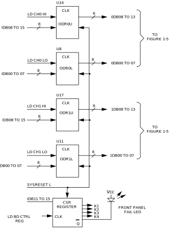
The DSC/DRC Board is designed with four 8-bit output data registers and a 5-bit CSR that controls the front panel Fail LED and relays for Built-in-Test, as shown in
[image:21.612.157.490.236.683.2]Figure 1-4 below. All registers are cleared at power-up by the VMEbus SYSRESET signal; therefore, all synchro/resolver outputs are disconnected from their loads, and the front panel Fail LED is illuminated at power-up.
Figure 1-4 Output Data and Control Registers Block Diagram
LD CH0 HI
8
6
0DB08 TO 13
LD CH0 LO IDB08 TO 15
CLK ODR0U CLK ODR0L 8 8
IDB00 TO 07
0DB00 TO 07
1DB08 TO 13 8
6 ODR1U
LD CH1 HI
TO FIGURE 1-5
TO FIGURE 1-5
LD CH1 LO
8
8
IDB00 TO 07
1DB00 TO 07 ODR1L
SYSRESET L
FRONT PANEL FAIL LED IDB11 TO 15
LD BD CTRL REG
Q IDB08 TO 15
22
1
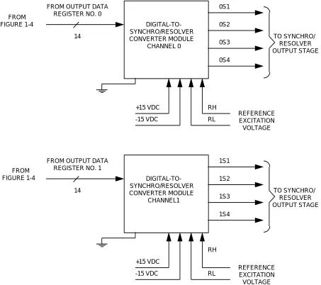
VMIVME-4905 Digital-to-Synchro/Resolver Converter BoardDigital-to-Synchro/Resolver Modules
[image:22.612.63.516.253.655.2]A functional block diagram of the synchro/resolver module is shown in Figure 1-5 below. The digital data provided as inputs to each module is stored in holding registers, as described in Output Data and Control Registers on page 21. VMIC selects from several vendors specific synchro/resolver modules that meet manufacturing options. The user should refer the Product Specification for a detailed explanation of available options.
Figure 1-5 Digital-to-Synchro/Resolver Block Diagram
FROM FIGURE 1-4
FROM OUTPUT DATA REGISTER NO. 0
DIGITAL-TO- SYNCHRO/RESOLVER CONVERTER MODULE
CHANNEL 0
TO SYNCHRO/ RESOLVER OUTPUT STAGE 0S1
0S2
0S3
0S4
RH RL +15 VDC
-15 VDC REFERENCE EXCITATION
VOLTAGE
FROM OUTPUT DATA REGISTER NO. 1
DIGITAL-TO- SYNCHRO/RESOLVER CONVERTER MODULE
CHANNEL1
TO SYNCHRO/ RESOLVER OUTPUT STAGE 1S1
1S2
1S3
1S4
RH
RL +15 VDC
-15 VDC REFERENCE EXCITATION
VOLTAGE FROM
FIGURE 1-4
Built-in-Test Hardware Operation
1
Built-in-Test Hardware Operation
The DSC/DRC Board supports fault detection and isolation when used with the VMIC SRTbus™ and VMIC's models VMIVME-4910 or VMIVME-4911. The SRTbus™ is a synchro/resolver test bus that utilizes the user I/O pins on the P2 VMEbus connector. Programming the proper control bits in the CSR of the VMIVME-4905 Board allows field disconnect and/or real-time loopback testing via the SRTbus™ and the VMIVME-4910 or VMIVME-4911 Boards.
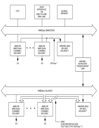
A typical VMIC DSC/DRC subsystem may be configured such that a VMIC P2 Synchro Backplane (SRTbus™) is utilized for isolating failures to the board level. The DSC/DRC Built-in-Test subsystem is based on an individually switched DSC/DRC output to a shared DSC/DRC Board, as shown in Figure 1-6 on page 24. This subsystem may be economically expanded by utilizing the VME repeater link, as shown in Figure 1-7 on page 25.
Each DSC/DRC Board is designed to support both off-line and on-line fault detection and isolation by program control of two Built-in-Test output control switches. During off-line testing, synchro/resolver outputs are physically disconnected from the loads. Connection to the test backplane is electrically interlocked, such that no two synchro outputs can be connected to the backplane simultaneously.
The VMIVME-4911 Quad SDC/RDC Board (Figure 1-8 on page 26) is utilized for fault detection and isolation of DSC/DRC Boards, and is based on an industry standard quad multiplexing Resolver/Synchro-to-Digital Converter (RDC/SDC) module. This high performance, fast settling, 14-bit SDC/RDC is required to support the real-time fault detection and isolation capabilities of the IIOC and the real-time
synchro/resolver input data processing required in the simulation and training industry.
VMIC also produces a model VMIVME-4910 tracking DSC/DRC Board (Figure 1-9 on page 27) that supports fault detection and isolation. The VMIVME-4910 is a
24
[image:24.612.74.508.142.414.2]1
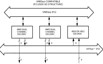
VMIVME-4905 Digital-to-Synchro/Resolver Converter BoardFigure 1-6 Built-in-Test Subsystem Configuration
4905 DUAL CHANNEL DSC/DRC
4905 DUAL CHANNEL DSC/DRC
4910 OR 4911 SDC/RDC
VMEbus (P1) VMEbus COMPATIBLE (P2 USER I/O STRUCTURE)
4 4
4
4 4 4
4 4
SRTbus™ (P2)
Built-in-Test Hardware Operation
1
Figure 1-7 Expanded Synchro/Resolver Subsystem with Built-in-Test
CPU
HOST INTERFACE
OR VME-TO-VME
DMA LINK
GLOBAL MEMORY
4900 OR 4905 DUAL CHANNEL DSC/DRC 4900 OR
4905 DUAL CHANNEL
DSC/DRC
VMEbus (MASTER)
SX SX SRTbus™ REPEATER VMIVME- TRANSPARENT
LINK
VMEbus (SLAVE)
4900 OR 4905 DUAL CHANNEL DSC/DRC
SX
4900 OR 4905 DUAL CHANNEL DSC/DRC
SX VMIC SYNCHRO/RESOLVER TEST BUS (TYP) (SRTbus™)
VMIVME-4910 OR 4911 SDC/RDC*
*The 4911 is required with systems configured with VMIC's IIOC (VMIVME-9016).
26
[image:26.612.97.501.148.654.2]1
VMIVME-4905 Digital-to-Synchro/Resolver Converter BoardFigure 1-8 Quad Channel DSC/DRC Board VMIVME-4911 Functional Block Diagram
P2 SRTbus ™ +5 VDC +15 VDC -15 VDC RH RL GND JUMPER SELECTABLE POWER AND REF INPUT OPTIONS +5 VDC +15 VDC -15 VDC RH RL GND
FIELD I/O CONNECTOR P3 SYNCHRO/ RESOLVER- TO-DIGITAL CONVERTER MODULE +5 VDC +15 VDC -15 VDC RH RL GND CSR DATA TRANS- CEIVERS 16
8- OR 16-BIT DATA TRANSFER 16 16 CONTROL LOGIC ADDRESS BUFFERS ADDRESS COMPARE ADDRESS SWITCHES SYNCHRO TEST BUS SIGNALS
Built-in-Test Hardware Operation
1
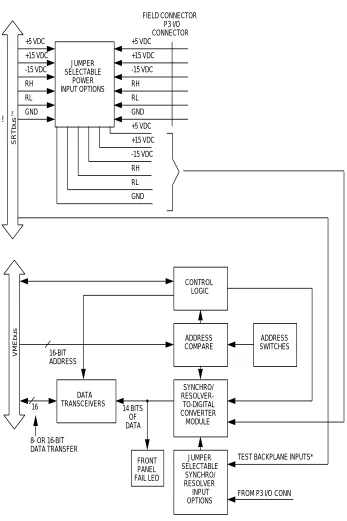
Figure 1-9 VMIVME-4910 Functional Block Diagram
SRTbus ™ JUMPER SELECTABLE POWER INPUT OPTIONS FIELD CONNECTOR P3 I/O CONNECTOR +15 VDC -15 VDC RH RL +15 VDC -15 VDC RH RL +15 VDC -15 VDC RH RL CONTROL LOGIC
8- OR 16-BIT DATA TRANSFER ADDRESS COMPARE ADDRESS SWITCHES VMEbus SYNCHRO/ RESOLVER- TO-DIGITAL CONVERTER MODULE 14 BITS OF DATA FRONT PANEL FAIL LED JUMPER SELECTABLE SYNCHRO/ RESOLVER INPUT OPTIONS
TEST BACKPLANE INPUTS*
FROM P3 I/O CONN
*Used for fault isolation of VMIVME-49XX Series DSC/DRC Boards. 16-BIT
ADDRESS
16
DATA TRANSCEIVERS
2 GND GND
GND
+5 VDC +5 VDC
28
1
VMIVME-4905 Digital-to-Synchro/Resolver Converter BoardOutput Relay Control
Four relays are provided to allow programmed field disconnect and to support real-time and off-line fault detection and isolation, as shown in Figure 1-10 below. The relays are controlled by the CSR, as described in Output Data and Control Registers on page 21. Relays K1 and K4 provide the field disconnect functions, whereas relays K2 and K3 provide the loopback testing hardware, as described in Built-in-Test Hardware
Operation on page 23. Relay control logic for relays K2 and K3 is designed with a
[image:28.612.125.451.290.694.2]hardware interlock to preclude simultaneous energization. Each synchro/resolver output is fused at the immediate outputs of the synchro/resolver module for overcurrent protection.
Figure 1-10 Synchro/Resolver Output Functional Block Diagram
CONVERTER CHANNEL 0 0S1 0S2 0S3 DSC/DRC NO. 0 TO SYNCHRO/RESOLVER BACKPLANE VIA P2
CONN S1 S2 S3 S4 P2 K2
NOTE: CONTROL LOGIC PROVIDES
HARDWARE LOCKOUT TO ENSURE THESE TWO RELAYS ARE NOT ACTIVATED AT THE SAME TIME.
K3 CHANNEL 1 SYNCHRO/RESOLVER OUTPUT TO P3 CONN
CONVERTER CHANNEL 1 1S1 1S2 1S3 K1 P3 CHANNEL 0 SYNCHRO/RESOLVER
OUTPUT TO P3 CONN
K4 P3
2.0 VA OR 5.0 VA OUTPUT DRIVE OPTION DSC/DRC NO. 1
TEST CHANNEL 0 OUT CHANNEL 0
TEST CHANNEL 1
OUT CHANNEL 1 2.0 VA OR 5.0 VA OUTPUT
Power Connections
1
Power Connections
[image:29.612.132.515.250.675.2]The dual-channel DSC/DRC Board is designed to use three DC power supplies and one reference signal as shown in Figure 1-11 below. External ±15 VDC power supplies are required. The user should refer to Product Specification for power requirements as a function of options ordered. Jumpers are provided, as shown in Figure 1-11, to provide the user an option to select front panel or rear panel 15 VDC and reference inputs.
Figure 1-11 Power Connection Block Diagram
VMEbus
P1
+5 VDC (VCC)
P2
P3 I/O CONNECTOR
+15 VDC
-15 VDC
RH
RL
+15 VDC
-15 VDC
RH
RL
DSC/DRCs VMEbus
H20 B
B
B
B C
C
C
C
A
A
A
A H19
H18
H17
DECOUPLING CAPACITORS
30
1
VMIVME-4905 Digital-to-Synchro/Resolver Converter Board5-Volt/Ampere Drive Option
This option provides the capability of driving up to 5-volt/amperes of torque
2-Volt/Ampere Output Isolation Transformer Option
1
2-Volt/Ampere Output Isolation Transformer Option
32
CHAPTER
Configuration and Installation
Contents
Unpacking Procedures . . . 34 Connector and Jumper/Configuration. . . 35 Built-in-Test Output Configuration. . . 41 Hardware Connection to Synchro or Resolver . . . 42 Built-in-Test Configuration with Synchro/Resolver Test Bus. . . 43 Address Modifiers . . . 44 Address Selection Switches . . . 45 Calibration of High Drive Capability Boards . . . 46
Introduction
This chapter describes the installation and configuration of the board. Cable configuration, jumper/switch configuration and board layout are illustrated in this chapter.
34
2
VMIVME-4905 Digital-to-Synchro/Resolver Converter BoardUnpacking Procedures
CAUTION: Some of the components assembled on VMIC’s products may be sensitive to electrostatic discharge and damage may occur on boards that are subjected to a high-energy electrostatic field. When the board is placed on a bench for configuring, etc., it is suggested that conductive material should be inserted under the board to provide a conductive shunt. Unused boards should be stored in the same protective boxes in which they were shipped.
Connector and Jumper/Configuration
2
Connector and Jumper/Configuration
Pin functions for the P2 and P3 connectors are listed in Table 2-1 on page 36. Jumper configurations for the ±15 VDC power and reference connection are shown in Table 2-2 on page 37. Factory configuration is shown in Table 2-3 on page 38, jumper locations are shown in Figure 2-1 on page 39.
NOTE: All other jumpers are option specific and should not be changed by user.
36
[image:36.612.143.435.131.502.2]2
VMIVME-4905 Digital-to-Synchro/Resolver Converter BoardTable 2-1 P2, P3 Pinout
SIGNAL P2 CONNECTOR P3 CONNECTOR
DIG. GND B12, B22, B31, C1
AND. GND A3, A4, 2, 24, 25 +15VDC
-15VDC RH
RL
0S1
0S2
0S3
0S4
1S1
1S2
1S3
1S4
C5, C6 C7, C8 C29 C27
13 11 14 16
1
3
5
7
18 20
22
9
S1*
C18 S2*
C20 S3*
C22
S4* C24
Connector and Jumper/Configuration
2
Table 2-2 Jumper Factory Configuration
JUMPER HIGH DRIVE CAPABILITY (POWER) OPTION H1 H2
H3 NOT INSTALLED
H5 H6 NOT INSTALLED INSTALLED H8 H9 H11 H12 INSTALLED NOT INSTALLED NOT INSTALLED INSTALLED H14 H15 H16 H17 H18 H19 H20 INSTALLED A B B B B B B C C C C C B B C C (4905-XXXX-5)
HIGH DRIVE CAPABILITY (POWER) OPTION WITH TRANSFORMER OPTION LOW DRIVE CAPABILITY (POWER) OPTION NOT INSTALLED NOT INSTALLED NOT INSTALLED NOT INSTALLED NOT INSTALLED NOT INSTALLED NOT INSTALLED A B B B B B B C C C C C B B C C (4905-XXXST-2) INSTALLED INSTALLED INSTALLED INSTALLED INSTALLED INSTALLED INSTALLED INSTALLED A B B B B B B C C C C C B B C C (4905-XXXX-02) NOT INSTALLED SYN RES
38
[image:38.612.139.437.136.686.2]2
VMIVME-4905 Digital-to-Synchro/Resolver Converter BoardTable 2-3 Jumper Configuration
JUMPER CONFIGURATION FUNCTION
H1 H2 H3 H4 H5 A B C B
CONNECTS CH1 RH TO P3 1RH CONNECTS CH1 RH TO CH0 RH
A B
C B
CONNECTS CH1 RL TO P3 1RL CONNECTS CH1 RL TO CH0 RL
FACTORY CONFIGURED TO BOARD OPTION
SEE SCHEMATIC SHEET 8 (USED TO BYPASS OP AMP CIRCUITRY)
H6 INSTALLED CONNECTS CH0 S3 TO OUTPUT RELAYS
H7 INSTALLED CONNECTS CH0 S2 TO OUTPUT RELAYS
H8 INSTALLED CONNECTS CH0 S1 TO OUTPUT RELAYS
H9 H10 H11
FACTORY CONFIGURED TO BOARD OPTION
SEE SCHEMATIC SHEET 8
(USED TO BYPASS OP AMP CIRCUITRY)
H12 INSTALLED CONNECTS CH1 S3 TO OUTPUT RELAYS
H13
H14
INSTALLED
INSTALLED
CONNECTS CH1 S2 TO OUTPUT RELAYS
CONNECTS CH1 S1 TO OUTPUT RELAYS
H15 A B
C B
CONNECTS RL TO CH0 RL OF CONVERTER MODULE
CONNECTS RH TO CH0 RL OF CONVERTER MODULE (RH, RL REVERSAL)
H16 C B
A B
CONNECTS RH TO CH0 RH OF CONVERTER MODULE
CONNECTS RL TO CH0 RH OF CONVERTER MODULE (RH, RL REVERSAL)
H17 A B
C B
CONNECTS P3 RL TO BOARD CONNECTS P2 RL TO BOARD
H18 A B
C B
CONNECTS P3 RH TO BOARD CONNECTS P2 RH TO BOARD
H19 A B
C B
CONNECTS P3 -15 V TO BOARD CONNECTS P2 -15 V TO BOARD
H20 A B
C B
CONNECTS P3 +15 V TO BOARD CONNECTS P2 +15 V TO BOARD
SYN
RES
FACTORY CONFIGURED TO BOARD OPTION
CONFIGURES CONVERTER MODULES FOR SYNCHRO OPERATION
FACTORY CONFIGURED
TO BOARD OPTION CONFIGURES CONVERTER MODULES FOR RESOLVER OPERATION
LOV FACTORY CONFIGURED TO BOARD OPTION FACTORY CONFIGURED TO BOARD OPTION
CONFIGURES CONVERTER MODULES FOR LOW VOLTAGE OPERATION HIV CONFIGURES CONVERTER MODULES
Conn ec tor an d J umper /Confi gur ati on
2
Fig u re 2 -1 S w itc h an d J u m p e r Lo cat ion sBOARD ADDRESS SWITCHES
S2
P1 P2
P3
H1
A B C
A B C H2 H3 H4 H5 H6 H7 H8 H9 H10 H11 H12 H13 H14 A B C A B C A B C
H15 H16 H17 H18 H19 A B C
H20 A B C SYN RES LOV HIV SYN LOV HIV SYN RES H21 H22 H23
H24 H25 H26 H27 H28
A B C
[image:39.612.70.710.124.522.2]40
2
VMIVME-4905 D igi tal -to -Sy nc h ro/R es ol ve r Conv er ter Bo ard JUMPER/ RESISTOR 1.3 Vrms (NOTE 3) 26 Vrms (NOTE 2) 115 Vrms (NOTE 3) 2-25 Vrms (NOTE 1) 27-114 Vrms (NOTE 1) 116-200 Vrms (NOTE 1) H21 H22 H23 H24 H25 H26 H27 H28 L0V H1V R1 R2 R3 R4 R5 R6 R7 R8 INSTALLED NOT INSTALLED INSTALLED NOT INSTALLED NOT INSTALLED INSTALLED NOT INSTALLED INSTALLED INSTALLED NOT INSTALLED NOT INSTALLED NOT INSTALLED NOT INSTALLED NOT INSTALLED NOT INSTALLED NOT INSTALLED NOT INSTALLED NOT INSTALLED NOT INSTALLED INSTALLED NOT INSTALLED INSTALLED INSTALLED NOT INSTALLED INSTALLED NOT INSTALLED NOT INSTALLED NOT INSTALLED NOT INSTALLED NOT INSTALLED NOT INSTALLED NOT INSTALLED NOT INSTALLED NOT INSTALLED NOT INSTALLED NOT INSTALLED INSTALLED INSTALLED INSTALLED INSTALLED INSTALLED INSTALLED INSTALLED INSTALLED NOT INSTALLED INSTALLED NOT INSTALLED NOT INSTALLED NOT INSTALLED NOT INSTALLED NOT INSTALLED NOT INSTALLED NOT INSTALLED NOT INSTALLED NOT INSTALLED NOT INSTALLED NOT INSTALLED NOT INSTALLED NOT INSTALLED NOT INSTALLED NOT INSTALLED NOT INSTALLED INSTALLED NOT INSTALLED INSTALLED NOT INSTALLED INSTALLED NOT INSTALLED NOT INSTALLED INSTALLED NOT INSTALLED INSTALLED NOT INSTALLED INSTALLED NOT INSTALLED INSTALLED INSTALLED NOT INSTALLED INSTALLED NOT INSTALLED NOT INSTALLED INSTALLED INSTALLED NOT INSTALLED NSTALLED NOT INSTALLED NOT INSTALLED INSTALLED NOT INSTALLED INSTALLED INSTALLED NOT INSTALLED INSTALLED NOT INSTALLED NOT INSTALLED INSTALLED NOT INSTALLED INSTALLED NOT INSTALLED INSTALLED NOT INSTALLED INSTALLED NOT INSTALLED INSTALLED INSTALLED NOT INSTALLED INSTALLED NOT INSTALLEDNOTES For non-standard reference input voltages contact factory for installation of R1 to R8 (requires new option number when ordering).
Factory configuration.
Factory configured upon request (new option number required when ordering). 1.
2.
[image:40.612.69.664.126.385.2]3.
Built-in-Test Output Configuration
2
Built-in-Test Output Configuration
[image:41.612.139.513.205.380.2]Relays are provided on the VMIVME-4905 to support off-line and real-time fault detection and isolation. The four relay functions are shown in Table 2-5 below.
Table 2-5 Relay Functions**
On power-up or on system reset, all relays are inactive.
*SRTbus™ is a synchro/resolver test bus, VMIVME-SRXX.
**Control hardware prevents test relays from being asserted at the same time. The asserted relay must be de-energized prior to asserting the other relay. The first one set has priority.
CSR BIT FUNCTION PERFORMED
14
13
12
11
OUT CH0
TEST CH0
OUT CH1
TEST CH1
CONNECTS D/S OR D/R CHAN 0 TO P3 FRONT PANEL CONNECTOR
CONNECTS D/S OR D/R CHAN 0 TO P2 CONNECTOR/SRTbus™*
CONNECTS D/S OR D/R CHAN 1 TO P3 FRONT PANEL CONNECTOR
CONNECTS D/S OR D/R CHAN 1 TO P2 CONNECTOR/SRTbus™*
42
2
VMIVME-4905 Digital-to-Synchro/Resolver Converter BoardHardware Connection to Synchro or Resolver
Depending on whether the board has Digital-to-Resolver Converter (DRC) or Digital-to-Synchro Converter (DSC) on-board, the pinouts in Connector and
Jumper/Configuration on page 35. Table 2-1 on page 36, are directly applicable to the
terminals labeled on the synchro or resolver load.
When driving a synchro load with the board, the S4 pins for channel No. 0 and channel No. 1 are not connected.
Built-in-Test Configuration with Synchro/Resolver Test Bus
2
Built-in-Test Configuration with Synchro/Resolver Test Bus
VMIC’s VMIVME-4911 Quad SDC/RDC Board interface is utilized for fault detection and isolation of DSC/DRC boards and is based on an industry standard
quad-multiplexing SDC/RDC module. This high performance, fast settling, 14-bit SDC/RDC is required to support the real-time fault detection and isolation capabilities of the IIOC and the real-time synchro/resolver input data processing required in the simulation and training industry.
VMIC also produces a model VMIVME-4910 tracking SDC/RDC Board that supports fault detection and isolation. The VMIVME-4910 is a single-channel synchro/resolver input board that is designed with input data switching relays to support either inputs from field sources via the front panel connector or the P2 VMEbus connector. It is also designed to support loopback testing of VMIC’s 49XX series DSC/DRC products. The worst-case settling time of the VMIVME-4910 may exceed 250 ms; therefore, it is not recommended for real-time data processing where update rates are in excess of the worst-case settling time. VMIC recommends the VMIVME-4911 Quad SDC/RDC Board for real-time simulation and training applications. This high-speed converter features simultaneous sampling and random access with a resolution of 14 bits and a 150 µs conversion time per channel.
The relay operation described in Built-in-Test Output Configuration on page 41
provides the user with the information necessary to implement built-in-test functions.
WARNING: This product must be used in a card cage with cooling fans in operation.
44
2
VMIVME-4905 Digital-to-Synchro/Resolver Converter BoardAddress Modifiers
Address Selection Switches
2
Address Selection Switches
[image:45.612.184.414.208.626.2]The VMIVME-4905 occupies 8 bytes of the VMEbus short I/O address space. The upper 13 address bits are switch selectable, as shown in Figure 2-2 below. The location of these switches are shown in Figure 2-1 on page 39.
Figure 2-2 Base Address Switches
ON
OFF OFF OFF OFF OFF
ON ON
1 2 3 4 5 6 7 8 A15 A14 A13 A12 A11 A10 A09 A08
8 F
DIP SWITCH
SW2
ON
OFF OFF OFF OFF ON
1 2 3 4 5 6 7 8 A07 A06 A05 A04 A03 AM2
0 7
DIP SWITCH
SW1
NOT USED
ON, CLOSED = 0 OFF, OPEN = 1
EXAMPLE
BASE ADDRESS = F870 = 1111 1000 0111 0XXX
A15 A03 AM2
46
2
VMIVME-4905 Digital-to-Synchro/Resolver Converter BoardCalibration of High Drive Capability Boards
All boards with the high drive capability option are calibrated at the factory to perform at the highest possible optimum level. It is not recommended that the user alter the set position of the calibration trim pots, doing so might cause
out-of-calibration readings. If calibration becomes necessary to the user, then the following procedure may be followed:
NOTE: The calibration trim pots (R17, R22, R31, R36) and the associated operational amplifiers (OP AMPs) (U2, U3, U4, U5, U6, U7) may be viewed in their existing locations on sheet 2 of 9 from the assembly drawing, Number 132-004905-000, available from VMIC..
NOTE: The following procedure should be followed only after the board has been configured (±15 V, RH, RL, etc.,) for normal operation.
Channel Zero
Step 1: Locate the OP AMP U2 and place a precision DC voltage meter on the output (case) of U2, thus providing a precision DC voltage reading between the output and ground. This will be referred to as the DC offset.
Step 2:With the DC offset from U2 recorded, locate the OP AMP U3 and place a precision DC voltage meter between the output (case) of U3 and ground.
Step 3:Locate the calibration trim pot R17 and alter the resistance value by trimming the pot to provide U3 with the same exact DC offset as was recorded for U2.
Step 4:Locate the OP AMP U4 and place a precision DC voltage meter between the output (case) of U4 and ground.
Step 5:Locate the calibration trim pot R22 and alter the resistance value by trimming the pot to provide U4 with the same exact DC offset as was recorded for U2.
Channel One
Step 6: Locate the OP AMP U5 and place a precision DC voltage meter on the output (case) of U5, thus providing a precision DC voltage reading between the output and ground. This will be referred to as the DC offset.
Step 7: With the DC offset from U5 recorded, locate the OP AMP U6 and place a precision DC voltage meter between the output (case) of U6 and ground.
Calibration of High Drive Capability Boards
2
Step 9: Locate the OP AMP U7 and place a precision DC voltage meter between the output (case) of U7 and ground.
48
CHAPTER
Programming
Contents
Built-in-Test Configuration with Synchro/Resolver Test Bus. . . 52
Introduction
An output operation is initiated by executing an output transfer instruction that loads one of two output registers. The execution of this instruction sends the VMEbus an address that causes selection of the Digital-to-Synchro/Resolver Converter
(DSC/DRC) Board if the board address switches match the address transmitted. The bit pattern of the data output word determines the position of the user’s torque receiver(s). The bit-to-angle conversion (position) information is shown in Table 3-1 on page 50.
The Central Processor Unit (CPU) should not initiate large shaft position changes that may result in overdriving the torque receiver(s). High current electrical transients and mechanical transients may damage the torque receiver and or the DSC/DRC Board. VMIC suggests that the user design synchro smoothing into a software driver. Smoothing is accomplished by incrementing to the desired angle.
The DSC/DRC Board is initialized at power-up with the field (user torque receivers) disconnected and the front panel Fail LED illuminated. The format and register addresses to control the relays, front panel Fail LED, and output torque receivers are shown in Table 3-2 on page 51. All VMIVME-4905 data output registers are write only and can be written as bytes or words.
THE Control and Status Register (CSR) Bits 11 and 13 Control the connection of the synchro outputs VIA RELAYS K2 AND K3 to the synchro backplane (see Figure 1-10 on page 28); therefore, only one of these relays can be energized at one time. The programmer must provide a one millisecond (minimum) delay for relays to drop out before another relay can be energized. Relays on other boards must also be
de-energized before they are tested. Simultaneous connection of more than one synchro signal to the test backplane can result in stuck relays and/or blown fuses.
50
3
VMIVME-4905 D igi tal -to -Sy nc h ro/R es ol ve r Conv er ter Bo ard BITNO. 2 (14-N)
[image:50.612.94.653.161.423.2]LSB AS % OF FULL SCALE RADIANS BIT DEGREES BIT MINUTES BIT SECONDS BIT MILS BIT
0
1
2
3
4
5
6
7
8
9
10
11
12
13
16,384.
8,192.
4,096.
2,048.
1,024.
512.
256.
128.
64.
32.
16.
8.
4.
2.
.00610352
.01220703
.02441406
.04882813
.09765625
.1953125
.390625
.78125
1.5625
3.125
6.25
12.5
25.
50.
.00038350
.00076699
.00153398
.00306796
.00613592
.01227185
.02454369
.04908739
.09817477
.19634954
.39269908
.78539816
1.57079633
3.14159265
.0219727
.0439453
.0878906
.1757813
.3515625
.703125
1.40625
2.8125
5.625
11.25
22.5
45.
90.
180.
1.31836
2.63672
5.27344
10.54688
21.09375
42.1875
84.375
168.75
337.5
675.
1,350.
2,700.
5,400.
10,800.
79.1016
158.2031
316.4063
632.8125
1,265.6250
2,531.25
5,062.5
10,125.
20,250.
40,500.
81,000.
162,000.
324,000.
648,000.
0.390625
0.78125
1.5625
3.125
6.25
12.5
25.
50.
100.
200.
400.
800.
1,600.
3,200.
3
Table 3-2 Address Map and Register Bit Formats
HEX ADDRESS
A3 A2 BINARY ADDRESS
D/S OR D/R NO. 0 OUTPUT REGISTER UPPER BYTE (WRITE ONLY)
D/S OR D/R NO. 0 OUTPUT REGISTER LOWER BYTE (WRITE ONLY)
D/S OR D/R NO. 1 OUTPUT REGISTER UPPER BYTE (WRITE ONLY)
D/S OR D/R NO. 1 OUTPUT REGISTER LOWER BYTE (WRITE ONLY)
CONTROL STATUS REGISTER UPPER BYTE A1 A0
A15 - A4
X X X X 0 0 0 BIT 15 BIT 14 BIT 13 BIT 12 BIT 11 BIT 10 BIT 9 BIT 8 NOT
USED
NOT
USED 0DB13 0DB12 0DB11 0DB10 0DB9 0DB8
X X X X 0 0 1 BIT 7 BIT 6 BIT 5 BIT 4 BIT 3 BIT 2 BIT 1 BIT 0
0DB5 0DB4 0DB3 0DB2 0DB1 0DB0
X X X X 0 1 0 BIT 15 BIT 14 BIT 13 BIT 12 BIT 11 BIT 10 BIT 9 BIT 8 NOT
USED
NOT
USED 1DB13 1DB12 1DB11 1DB10 1DB9 1DB8
X X X X 0 1 1 BIT 7 BIT 6 BIT 5 BIT 4 BIT 3 BIT 2 BIT 1 BIT 0
1DB5 1DB4 1DB3 1DB2 1DB1 1DB0
1DB6 1DB7
X X X X 1 0 0 BIT 15 BIT 14 BIT 13 BIT 12 BIT 11 BIT 10 BIT 9 BIT 8 FL=1 (R/W) OUT CH0 (R/W) NOT USED (FLOATING) TEST CH0 (R/W) OUT CH1 (R/W) TEST CH1 (R/W)
CONTROL STATUS REGISTER LOWER BYTE
X X X X 1 0 1 BIT 7 BIT 6 BIT 5 BIT 4 BIT 3 BIT 2 BIT 1 BIT 0
NOT USED
A15 A3
Base address switch selectable
FL=Front panel Fail LED 0=On
1=Off
Fail LED is turned ON at power-up or system reset.
All register bits are cleared at power-up or system reset, which also de-energizes the relays.
52
3
VMIVME-4905 Digital-to-Synchro/Resolver Converter BoardBuilt-in-Test Configuration with Synchro/Resolver Test Bus
VMIC’s VMIVME-4911 Quad SDC/RDC interface is utilized for fault detection and isolation of DSC/DRC Boards and is based on an industry standard
quad-multiplexing SDC/RDC module. This high performance, fast settling, 14-bit SDC/RDC Board is required to support the real-time fault detection and isolation capabilities of the IIOC and the real-time synchro/resolver input data processing required in the simulation and training industry.
The relay operation described in the following section provides the user with the information necessary to implement built-in-test functions.
Built-in-Test Output Configuration
[image:52.612.103.479.338.515.2]Relays are provided on the VMIVME-4905 to support off-line and real-time fault detection and isolation. The four relay functions are shown in Table 3-3 below.
Table 3-3 Relay Functions
On power-up or on system reset, all relays are inactive.
*SRTbus™ is a synchro/resolver test bus, VMIVME-SRXX.
CSR BIT FUNCTION PERFORMED
14
13
12
11
OUT CH0
TEST CH0
OUT CH1
TEST CH1
CONNECTS D/S OR D/R CHAN 0 TO P3 FRONT PANEL CONNECTOR
CONNECTS D/S OR D/R CHAN 0 TO P2 CONNECTOR/SRTbus*
CONNECTS D/S OR D/R CHAN 1 TO P3 FRONT PANEL CONNECTOR
CONNECTS D/S OR D/R CHAN 1 TO P2 CONNECTOR/SRTbus™
Maintenance
Maintenance
This section provides information relative to the care and maintenance of VMIC’s products. If the product malfunctions, verify the following:
• System power • Software
• System configuration • Electrical connections
• Jumper or configuration options
• Boards are fully inserted into their proper connector location • Connector pins are clean and free from contamination
• No components of adjacent boards are disturbed when inserting or removing the board from the chassis
• Quality of cables and I/O connections
If products must be returned, contact VMIC for a Return Material Authorization (RMA) Number. This RMA Number must be obtained prior to any return.
VMIVME-4905 Digital-to-Synchro/Resolver Converter Board
54


methanone](data:image/gif;base64,R0lGODlhAQABAIAAAP///wAAACH5BAEAAAAALAAAAAABAAEAAAICRAEAOw==)