http://go.warwick.ac.uk/lib-publications
Original citation:
Guell, Aleix G., Ebejer, Neil, Snowden, Michael E., Macpherson, Julie V. and Unwin,
Patrick R.. (2012) Structural correlations in heterogeneous electron transfer at
monolayer and multilayer graphene electrodes. Journal of the American Chemical
Society, Vol.134 (No.17). pp. 7258-7261. ISSN 0002-7863
Permanent WRAP url:
http://wrap.warwick.ac.uk/50301/
Copyright and reuse:
The Warwick Research Archive Portal (WRAP) makes the work of researchers of the
University of Warwick available open access under the following conditions. Copyright ©
and all moral rights to the version of the paper presented here belong to the individual
author(s) and/or other copyright owners. To the extent reasonable and practicable the
material made available in WRAP has been checked for eligibility before being made
available.
Copies of full items can be used for personal research or study, educational, or
not-for-profit purposes without prior permission or charge. Provided that the authors, title and
full bibliographic details are credited, a hyperlink and/or URL is given for the original
metadata page and the content is not changed in any way.
Publisher’s statement:
This document is the unedited Author’s version of a Submitted Work that was
subsequently accepted for publication in Journal of the American Chemical Society, ©
American Chemical Society after peer review. To access the final edited and published
work see
http://dx.doi.org/10.1021/ja3014902
A note on versions:
The version presented here may differ from the published version or, version of record, if
you wish to cite this item you are advised to consult the publisher’s version. Please see
the ‘permanent WRAP url’ above for details on accessing the published version and note
that access may require a subscription.
Structural Correlations in Heterogeneous Electron Transfer at
Monolayer and Multilayer Graphene Electrodes
Aleix G. G
ü
ell, Neil Ebejer, Michael E. Snowden, Julie V. Macpherson and Patrick R. Unwin*
Department of Chemistry, University of Warwick, Coventry, CV4 7AL, United Kingdom Graphene, Electrochemistry, Imaging
Supporting Information Placeholder
ABSTRACT: As a new form of carbon, graphene is attracting intense interest as an electrode material with widespread ap-plications. In the present study, the heterogeneous electron transfer (ET) activity of graphene is investigated using scan-ning electrochemical cell microscopy (SECCM), which allows electrochemical currents to be mapped at high spatial resolu-tion across a surface for correlaresolu-tion with the corresponding structure and properties of the graphene surface. We establish that the rate of heterogeneous ET at graphene increases sys-tematically with the number of graphene layers, and show that the stacking in multilayers also has a subtle influence on ET kinetics.
Graphene-based materials are having a huge impact in elec-trochemistry and electrochemical technologies, with promising applications in areas such as supercapacitors,1 batteries,2 elec-trocatalytic supports,3 sensors for electroanalysis4 and trans-parent electrodes.5 These important technologies typically use graphene produced by chemical vapor deposition (CVD)6 and other scalable methods, yet important fundamentals questions concerning heterogeneous electron transfer (ET) at such mate-rials –intrinsic to many of these applications- remain to be addressed. Electrical measurements have revealed that the electron mobility7 and the electronic band structure8 are sensi-tive to the number of graphene layers and their stacking order, with implications for electrochemistry. In this communication, we thus seek to elucidate how both the number of graphene layers and arrangement of the layers influence heterogeneous ET kinetics.
Graphene grown by CVD on nickel substrates9 (see Sup-porting Information section 1) was optimal for the present study because it presents a heterogeneous continuous layer of microsized multilayered flakes, which can be addressed with high resolution scanning electrochemical cell microscopy (SECCM).10-13 Thus, on one sample it is possible to make thousands of individual electrochemical (EC) measurements at different locations and relate these to the corresponding gra-phene structure. This provides datasets on a scale that would be unfeasible with conventional photolithographic techniques of the type employed in recent EC studies of exfoliated gra-phene.14-16 In order to study the unambiguous electrochemical response of graphene without any interference from a conduc-tive substrate, CVD graphene layers were transferred to a sili-con substrate with a 300 nm thermal grown oxide layer. This substrate allowed optical visualization and identification of the morphological film features characteristic of graphene,17,18 for
direct correlation with the local electrochemistry. Importantly, the approach described herein makes possible the study of graphene surfaces with minimal intrusion and avoids the need for any post-processing lithographic step, which may result in unavoidable damage and possible interference of residues.19
A finite element model12 was developed to analyze the EC maps (Supporting Information section 3) and extract and as-sign standard heterogeneous ET rate constants at each
mi-cron-scale pixel of the images. For each pixel, we assumed
[image:3.612.79.522.71.305.2]reasonably the
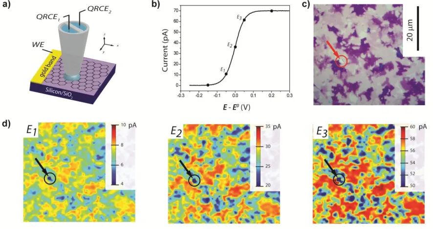
Figure 1: SECCM. (a) Schematic representation of the EC imaging setup. The graphene lies on a Si/SiO2 substrate and is connected as the
working electrode via an evaporated Cr/Au band. A SECCM probe is employed as a local and mobile EC cell for electrochemical imaging. (b) LSV for the oxidation of 2mM FcTMA+ (30 mM KCl) acquired with a SECCM setup on a graphene surface, at 100 mV s-1, with a ≈1
m diameter pipet. (c) Optical microscope image of the CVD graphene area mapped by SECCM, showing the heterogeneity of the surface and the presence of multiple-layer graphene flakes. (d) Set of three EC maps of the area shown in c) acquired by SECCM at three different substrate electrode potentials (E – Eo)indicated in the LSV in b) with labels E1, E2 and E3. All images are at the same scale as c). The ar-row-circle in part c) and d) indicates a small area where the silicon oxide was exposed and measured currents in this area are below the lower limit on the scale bar. This area was used to calibrate the number of graphene layers (Supporting Information Section 5).
Butler-Volmer model for ET22 and a uniformly active surface given the tiny area investigated. Electrochemical kinetic anal-yses are relatively insensitive to the value of the transfer coef-ficient for α = 0.5 ± 0.2 (ref 23) and so we chose α = 0.5, giv-en the large self exchange ET rate constant for ferrocgiv-ene and its derivatives.24
Comparison between the observed heterogeneity in EC ac-tivity of CVD graphene and the corresponding topography, revealed by optical microscopy or atomic force microscopy (AFM) (Supporting Information section 4) shows a clear cor-relation between electrochemical activity and the number of graphene layers. Qualitatively, there is close correspondence between dark regions (multilayers) in Figure 1c and high EC currents (Figure 1d and Supporting Information section 2).
In order to examine this relationship in more detail, EC cur-rent maps and the optical image were correlated quantitatively. Given the linear increase of green component contrast with the number of graphene layers,9,17,18 and with further confirmation from micro-Raman spectroscopy (vide infra), the full range of light contrast was segmented into 8 different bins assigned to a defined number of graphene layers (see Supporting Infor-mation section 5).
Figure 2a shows the local EC current at potential E2 versus the number of graphene layers. Similar correlations at poten-tials E1 and E3 are provided in Supporting Information section 2. From this plot, it is clear that single layer graphene exhibits the lowest EC activity, and that the activity increases systemat-ically with the number of layers, to a situation where the flakes are so active that the ET process becomes essentially
reversi-ble13 within experimental error (see Supporting Information, Figure S9).
EC current distributions were analyzed to obtain the corre-sponding ET standard rate constants (k0) for potentials E1, E2 and E3 (full details in ref 12 and Supporting Information sec-tion 3). Figure 2b reveals that the ET kinetics evolves with the number of layers towards faster ET and a broader range of k0 (and current magnitudes) from monolayer to multilayer gra-phene. This is found consistently at all three potentials. Alt-hough there will be some cross contribution of different flakes at some single point measurements (where the tip is at the boundary between flakes), the different stacking order within the graphene multilayers could also play a role in the broad-ness of ET kinetics, seen for bilayer, trilayer and thicker flakes, especially for epitaxial of CVD multilayer graphene, where non-Bernal or AB stacking order is very common.25
for the 2D peak (Figure 3d), in addition to light contrast values of 0.15 (Supporting information section 5), indicate that the A2 region actually corresponds to a non-AB stacking bilayer. The lack of AB stacking (Figure 3d) reduces electronic cou-pling between the graphene layers, so that bilayer graphene in
this configuration has electronic properties similar to that of monolayer graphene.30-32 This evidently impacts directly the EC activity: current values for the A2 spot are very similar to
the A1 region (Figure 3b and
Figure 2: (a) Pixel-by-pixel correlation between the EC current map at potential E2 and the number of graphene layers. (b) Histograms of the EC current and standard rate constant, k0, for each defined number of CVD graphene layers, for potentials E1, E2 and E3 (from left to right). The dashed line in a) and the blue area in b) denotes the conditions where the ET process becomes entirely reversible.
Supporting Information section 6), which corresponds to a single layer. It is accepted that the electronic structure and density of states play a key role in heterogeneous ET rates,22,33 and these results show that different graphene layers (mono-layer and bi(mono-layer), with closely similar band structures, behave analogously in terms of electrochemistry. This result also allows us to rule out a strong influence of charge carrier mo-bility to the electrochemical activity measured. An increase of mobility is expected for a non-AB stacking bilayer, compared to monolayer graphene, since the substrate effect is, to some extent, screened by the additional graphene layer beneath the top layer in the case of bilayer graphene34 but this does not enhance ET kinetics compared to the intrinsic activity of mon-olayer graphene.
The areas A3 and A4 are assigned to trilayer and multilayer (>trilayer), respectively, based on the much broader 2D peak (Figure 3e) and the intensity and peak position of the G peak
(Figure 3c). For these domains, an increase of EC activity is observed with the number of layers (Figure 3b), consistent with the evolution of the density of electronic states through single layer, AB-bilayer and trilayer graphene.7 These more detailed analyses (Figure 3b and Supporting Information sec-tion 6) confirm the trend (vide supra) between EC current and light contrast in the optical image (interpreted as the number of graphene layers).
[image:4.612.61.556.107.274.2]Figure 3: (a) Optical image of CVD graphene with 4 different flakes labeled A1, A2, A3 and A4, and corresponding SECCM data. Scale bar is 5 m. (b) Histograms of the EC current in each designated flake at potential E2. (c) Raman spectra acquired with an excitation wave-length of 633 nm and spot size of 500 nm at each graphene flake. The three characteristic Raman peaks for graphene are labelled as D, G and 2D. (d) Raman 2D peak for regions A1 (red line) and A2 (blue line) plotted together highlighting the ≈10 cm-1
Raman upshift charac-teristic for a non-AB stacking bilayers (blue line). Schematic of Bernal (AB-stacking) for a bilayer of graphene. The basic structure of graphene is defined with two atoms in the unit cell, denoted A (red dot) and B (blue dot). For an AB stacking bilayer, the A atom of the top layer lies directly over the B atom of the bottom layer. (e) The Raman 2D peak for areas A1 (red line), A3 (green line) and A4 (orange line)
they are responsible for local changes in the electronic struc-ture,35 but were essentially uniform (as evidenced by AFM in Supporting Information) over the entire surface area and inde-pendent of the number of layers and flakes. The Raman D peak at 1350 cm-1 is usually used to determine the density of defects on graphene,26,27 either as the peak intensity itself, or with the ratio of D and G peaks (ID/IG). In all spectra obtained,
the D peak intensity was essentially constant for all flakes studied and independent of the number of layers. Indeed, if the ID/IG ratios are compared, the multilayered flakes have the
lowest density of defects, yet have higher activity. It is further well known36,37 that edges accumulate a higher density of de-fects, but it is clear that we see no increase of EC activity along the edges of either the flakes or at the (step-edge) boundary between flakes, at the spatial resolution of the inves-tigation.
In conclusion, we have demonstrated how the ET activity of a complex graphene material can be elucidated, analyzed and correlated with intrinsic structural properties using high reso-lution SECCM in tandem with Raman microscopy, optical microscopy and AFM. The unprecedented insights on the structural controls of ET are of fundamental value, and pro-vide a rational basis for the design and use of graphene in electrochemical technologies. The SECCM methodology de-scribed is general and we expect it will find increasing use for structure – function imaging of surface and interfacial pro-cesses.
ASSOCIATED CONTENT
Supporting Information. Full experimental details of graphene synthesis, SECCM operation and complementary maps, AFM images, light contrast calibration and FEM simulations. This ma-terial is available free of charge via the Internet at http://pubs.acs.org.
AUTHOR INFORMATION
Corresponding Author [email protected]
ACKNOWLEDGMENT
This project was supported by the European Research Council through project ERC-2009-AdG 247143-QUANTIF and a Marie Curie IntraEuropean Fellowship (236885) (A.G.G). Funding from the EPSRC (EP/H023909/1) and UK National Physical Laborato-ry it is also acknowledged. Equipment used in this research was obtained through Science City (AM2), with support from Ad-vantage West Midlands and part funded by the European regional Development Fund. The authors thank Mr. Kim McKelvey for assistance in data analysis and Mr. Tom Miller and Mr. Anatolii Kuharuk for contributions to CVD graphene synthesis.
REFERENCES
(1) Zhu, Y.; Murali, S.; Stoller, M. D.; Ganesh, K. J.; Cai, W.; Ferreira, P. J.; Pirkle, A.; Wallace, R. M.; Cychosz, K. A.; Thommes, M.; Su, D.; Stach, E. A.; Ruoff, R. S. Science2011, 332, 1537.
(2) Xiao, J.; Mei, D.; Li, X.; Xu, W.; Wang, D.; Graff, G. L.; Bennett, W. D.; Nie, Z.; Saraf, L. V.; Aksay, I. A.; Liu, J.; Zhang, J.-G. Nano Lett.2011, 11, 5071.
(3) Liang, Y.; Li, Y.; Wang, H.; Zhou, J.; Wang, J.; Regier, T.; Dai, H. Nature Mater.2011, 10, 780.
(4) Schedin, F.; Geim, A. K.; Morozov, S. V.; Hill, E. W.; Blake, P.; Katsnelson, M. I.; Novoselov, K. S. Nature Mater.2007, 6, 652.
(5) Bonaccorso, F.; Sun, Z.; Hasan, T.; Ferrari, A. C. Nature Photon.2010, 4, 611.
(6) Bae, S.; Kim, H.; Lee, Y.; Xu, X.; Park, J.-S.; Zheng, Y.; Balakrishnan, J.; Lei, T.; Ri Kim, H.; Song, Y. I.; Kim, Y.-J.; Kim, K. S.; Ozyilmaz, B.; Ahn, J.-H.; Hong, B. H.; Iijima, S. Nature Nanotech.2010, 5, 574.
(7) Zhu, W.; Perebeinos, V.; Freitag, M.; Avouris, P. Phys Rev B2009, 80, 235402.
(8) Bao, W.; Jing, L.; Velasco, J.; Lee, Y.; Liu, G.; Tran, D.; Standley, B.; Aykol, M.; Cronin, S. B.; Smirnov, D.; Koshino, M.; McCann, E.; Bockrath, M.; Lau, C. N. Nature Phys.2011, 7, 948.
(9) Reina, A.; Jia, X.; Ho, J.; Nezich, D.; Son, H.; Bulovic, V.; Dresselhaus, M. S.; Kong, J. Nano Lett.2009, 9, 30.
(10) Ebejer, N.; Schnippering, M.; Colburn, A. W.; Edwards, M. A.; Unwin, P. R. Anal. Chem.2010, 82, 9141.
(11) Lai, S. C.; Dudin, P. V.; Macpherson, J. V.; Unwin, P. R. J. Am. Chem. Soc.2011, 133, 10744.
(12) Snowden, M. E.; Guell, A. G.; Lai, S. C.; McKelvey, K.; Ebejer, N.; O'Connell, M. A.; Colburn, A. W.; Unwin, P. R. Anal. Chem.2012, 84, 2483.
(13) Lai, S. C. S.; Patel, A. N.; McKelvey, K..; Unwin, P. R.;
Angew. Chem. Intl. Ed. Eng.2012, doi: 10.1002/201200564. (14) Xia, J.; Chen, F.; Li, J.; Tao, N. Nature Nanotech.2009, 4, 505.
(15) Li, W.; Tan, C.; Lowe, M. A.; Abruña, H. c. D.; Ralph, D. C. ACS Nano2011, 5, 2264.
(16) Valota, A. T.; Kinloch, I. A.; Novoselov, K. S.; Casiraghi, C.; Eckmann, A.; Hill, E. W.; Dryfe, R. A. W. ACS Nano2011, 5, 8809
(17) Blake, P.; Hill, E. W.; Neto, A. H. C.; Novoselov, K. S.; Jiang, D.; Yang, R.; Booth, T. J.; Geim, A. K. Appl. Phys. Lett.2007,
91, 063124.
(18) Ni, Z. H.; Wang, H. M.; Kasim, J.; Fan, H. M.; Yu, T.; Wu, Y. H.; Feng, Y. P.; Shen, Z. X. Nano Lett.2007, 7, 2758.
(19) Dudin, P. V.; Snowden, M. E.; Macpherson, J. V.; Unwin, P. R. ACS Nano2011, 5, 10017.
(20) Heller, I.; Kong, J.; Heering, H. A.; Williams, K. A.; Lemay, S. G.; Dekker, C. Nano Lett.2004, 5, 137.
(21) Rodolfa, K. T.; Bruckbauer, A.; Zhou, D.; Korchev, Y. E.; Klenerman, D. Angew. Chem. Intl. Ed. Engl.2005, 44, 6854.
(22) Bard, A. J.; Faulkner, L. Electrochemical methods: fundamentals and applications; Wiley: Weinheim, 2001.
(23) Mirkin, M. V.; Bard, A. J. Anal. Chem.1992, 64, 2293. (24) Nielson, R. M.; McManis, G. E.; Safford, L. K.; Weaver, M. J. J. Phys. Chem.1989, 93, 2152.
(25) Pimenta, M. A.; Dresselhaus, G.; Dresselhaus, M. S.; Cancado, L. G.; Jorio, A.; Saito, R. Phys. Chem. Chem. Phys.2007,
9, 1276.
(26) Ferrari, A. C.; Meyer, J. C.; Scardaci, V.; Casiraghi, C.; Lazzeri, M.; Mauri, F.; Piscanec, S.; Jiang, D.; Novoselov, K. S.; Roth, S.; Geim, A. K. Phys. Rev. Lett.2006, 97, 187401.
(27) Malard, L. M.; Pimenta, M. A.; Dresselhaus, G.; Dresselhaus, M. S. Phys. Rep.2009, 473, 51.
(29) Ni, Z.; Wang, Y.; Yu, T.; You, Y.; Shen, Z. Phys. Rev. B.
2008, 77, 235403.
(30) Lopes dos Santos, J. M. B.; Peres, N. M. R.; Castro Neto, A. H. Phys. Rev. Lett.2007, 99, 256802.
(31) Latil, S.; Meunier, V.; Henrard, L. Phys. Rev. B.2007, 76, 201402.
(32) Hass, J.; Varchon, F.; Millán-Otoya, J. E.; Sprinkle, M.; Sharma, N.; de Heer, W. A.; Berger, C.; First, P. N.; Magaud, L.; Conrad, E. H. Phys. Rev. Lett.2008, 100, 125504.
(33) Heller, I.; Kong, J.; Williams, K. A.; Dekker, C.; Lemay, S. G. J. Am. Chem. Soc.2006, 128, 7353.
(34) Ohta, T.; Bostwick, A.; McChesney, J. L.; Seyller, T.; Horn, K.; Rotenberg, E. Phys. Rev. Lett.2007, 98, 206802.
(35) Xu, K.; Cao, P.; Heath, J. R. Nano letters2009, 9, 4446. (36) Graf, D.; Molitor, F.; Ensslin, K.; Stampfer, C.; Jungen, A.; Hierold, C.; Wirtz, L. Nano Lett.2007, 7, 238.