http://www.scirp.org/journal/msce ISSN Online: 2327-6053
ISSN Print: 2327-6045
DOI: 10.4236/msce.2018.64015 Apr. 30, 2018 147 Journal of Materials Science and Chemical Engineering
Guidelines for Optimization of the Absorber
Layer Energy Gap for High Efficiency
Cu(In,Ga)Se
2
Solar Cells
N. Severino, N. Bednar, N. Adamovic
Institute of Sensor and Actuator Systems, Technische Universität Wien, Vienna, Austria
Abstract
This work investigates in-depth the effects of variation of the compositional ratio of the absorber layer in Cu(In,Ga)Se2 (CIGS) thin-film solar cells.
Elec-trical simulations were carried out in order to propose the most suitable gal-lium double-grading profile for the high efficiency devices. To keep the model as close as possible to the real behavior of the thin film solar cell a trap model was implemented to describe the bulk defects in the absorber layer. The per-formance of a solar cell with a standard CIGS layer thickness (2 μm) exhibits a strong dependence on the front grading height (decreasing band gap toward the middle of the CIGS layer). An absolute gain in the efficiency (higher than 1%) is observed by a front grading height of 0.22. Moreover, simulation re-sults show that the position of the plateau (the region characterized by the minimum band gap) should be accurately positioned at a compositional ratio of 20% Ga and 80% In, which corresponds to the region where a lower bulk defect density is expected. The developed model demonstrates that the length of the plateau is not playing a relevant role, causing just a slight change in the solar cell performances. Devices with different absorber layer thicknesses were simulated. The highest efficiency is obtained for a CIGS thin film with thick-nesses between 0.8 and 1.1 μm.
Keywords
Solar Cell, Thin-Film, Simulation, Material Modelling
1. Introduction
Among thin-film technologies, solar cells and modules based on the polycrystal-line Cu(In,Ga)Se2 (CIGS) absorber layer are one of the most advanced and
effi-How to cite this paper: Severino, N., Bednar, N. and Adamovic, N. (2018) Guidelines for Optimization of the Absor-ber Layer Energy Gap for High Efficiency Cu(In,Ga)Se2 Solar Cells. Journal of Mate-rials Science and Chemical Engineering, 6, 147-162.
https://doi.org/10.4236/msce.2018.64015
Received: February 15, 2018 Accepted: April 27, 2018 Published: April 30, 2018
Copyright © 2018 by authors and Scientific Research Publishing Inc. This work is licensed under the Creative Commons Attribution International License (CC BY 4.0).
DOI: 10.4236/msce.2018.64015 148 Journal of Materials Science and Chemical Engineering
cient. Efficiencies higher than 22% have been reported on the cell level [1]. The module efficiencies around 19% have been measured and confirmed under standard conditions (AM1.5 spectrum at 25˚C) [1].
CIGS is a versatile material and products based on this semiconductor can access different markets. On one side CIGS glass-encapsulated modules can an-swer the demand of the well-established PV market based on classical PV appli-cations (e.g. power plants and roof-top installations). On the other side there are significant efforts to develop flexible, lighter and durable modules with better integration capabilities, for the emerging applications in building and product integrated PV.
What makes CIGS an attractive absorber layer compared to silicon, is that it is a direct band gap material characterized by a high absorption coefficient, which allows the decrease of the absorber layer thickness; high stability and high effi-ciency devices with thicknesses between 1 - 2 µm can be readily obtained [2].
CIGS thin film can be grown using different vacuum and non-vacuum tech-niques (e.g. evaporation, sputtering, electrochemical deposition, nanoparticle printing and ion-beam deposition) [3][4][5][6] [7]. Devices with the highest performances are fabricated by a multi-stage co-evaporation process, known as the “three-stage process” [8]. This deposition technique results in a double-graded composition profile characterized by higher Ga content towards the back and the front of the film, and a plateau of low Ga content in between
[9][10]. Such controlled variable semiconductor composition represents an at-tractive possibility to tune the semiconductor’s band gap, which can be graded over a wide range by varying the [Ga]/([In] + [Ga]) ratio in the thin film layer during the growth process [11][12][13].
However, besides its interesting properties, this semiconductor compound results in a complex structure, due to the large number of layers those constitute the final solar cell. In order to allow the selection of the most suitable solar cell structure, which is able to achieve higher conversion efficiencies and to fully understand the fundamental physics behavior of the device, it is needed to de-velop numerical models which will include the described peculiarities of the ma-terial. Simulations based upon these models will reduce the number of technolo-gical experiments and enable faster and inexpensive optimization of the devices.
In this paper we analyzed and reviewed the most suitable characteristics of the CIGS absorber layer in order to reach high efficiency devices. In particular an in-depth analysis of gallium double-grading strategy was carried out. Thus, it can provide the support to the technology development.
2. Simulation Set-Up
DOI: 10.4236/msce.2018.64015 149 Journal of Materials Science and Chemical Engineering
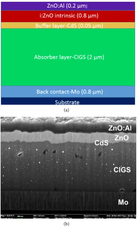
of the following layers: substrate (glass or polyimide)/Mo/CIGS/CdS/TCO. Two layers of ZnO and ZnO:Al form the transparent conductive oxide (TCO) of the solar cell. Characterized by high band gaps, these materials are transparent to the most of the solar spectrum. The chemical bath deposited CdS film is em-ployed as buffer layer in the high efficiency CIGS solar cell [16][17]. This ma-terial can uniformly and entirely cover the rough surface of the CIGS film avoiding the formation of shunt paths [18]. Additionally, the use of a buffer layer leads to the creation of an efficient p-n junction in CIGS/CdS/ZnO. A fa-vorable band alignment can be observed when a CdS buffer layer is used [19] [20][21]. A thin CIGS film, serves as the absorber (photoactive) layer. Mo was used as the back electrode. A part of the Mo layer is converted to MoSe2 when
CIGS layer is deposited at high temperature. The MoSe2 contributes to the
im-provement of adhesion at the CIGS/Mo interface and plays a significant role in the formation of a favorable ohmic contact [22]. A summary of the physical pa-rameters used in the model is shown in Table 1. The device architecture of the simulated CIGS solar cell is presented in Figure 1(a), Figure 1(b) shows an SEM analysis of cross section of the device.
[image:3.595.208.537.408.713.2]Considering initially a uniform band-gap (Eg) CIGS solar cell with an absor-ber layer thickness of 2 µm, the Eg was uniformly varied within the whole ab-sorber layer depth according to Equation (1) [23].
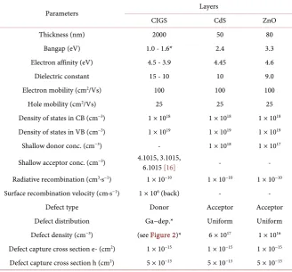
Table 1. Summary of the physical parameters used for the simulation model.
Parameters Layers
CIGS CdS ZnO
Thickness (nm) 2000 50 80
Bangap (eV) 1.0 - 1.6* 2.4 3.3
Electron affinity (eV) 4.5 - 3.9 4.45 4.6
Dielectric constant 15 - 10 10 9.0
Electron mobility (cm2/Vs) 100 100 100
Hole mobility (cm2/Vs) 25 25 25
Density of states in CB (cm−3) 1 × 10¹⁸ 1 × 10¹⁸ 1 × 10¹⁸
Density of states in VB (cm−3) 1 × 10¹⁹ 1 × 10¹⁹ 1 × 10¹⁹
Shallow donor conc. (cm−3) - 1 × 10¹⁸ 1 × 10¹⁷
Shallow acceptor conc. (cm−3) 4.1015, 3.1015,
6.1015 [16] - -
Radiative recombination (cm3·s−1) 1 × 10⁻¹⁰ 1 × 10⁻¹⁰ 1 × 10⁻¹⁰
Surface recombination velocity (cm·s−1) 1 × 10⁶ (back) - -
Defect type Donor Acceptor Acceptor
Defect distribution Ga−dep.* Uniform Uniform
Defect density (cm−3) (see Figure 2)* 6 × 1017 1 × 10¹⁶
Defect capture cross section e- (cm2) 1 × 10⁻¹⁵ 1 × 10⁻¹⁵ 1 × 10⁻¹⁵
Defect capture cross section h (cm2) 5 × 10⁻¹³ 5 × 10⁻¹³ 5 × 10⁻¹³
DOI: 10.4236/msce.2018.64015 150 Journal of Materials Science and Chemical Engineering (a)
[image:4.595.258.496.68.463.2](b)
Figure 1. (a) Device architecture of the simulated CIGS solar cell; (b) Cross-section of the CIGS solar cell, obtained by SEM.
(
)
(
)
CIGS CIS CGS
g g g
E =E 1 GGI− +GGI E⋅ − ⋅b GGI 1-GGI (1)
where CIS g
E = 1.01 eV and ECGSg = 1.636 eV are band-gaps of CIS and CGS,
respectively; GGI = [Ga]/([Ga] + [In]) and represents the compositional ratio and b is the optical bowing coefficient. Values between 0.11 and 0.24 have been reported for this parameter [17].
varia-DOI: 10.4236/msce.2018.64015 151 Journal of Materials Science and Chemical Engineering
tion of the compositional ratio was also considered. The data reported in the work of Paulson et al. [27], regarding the measured α values for different Ga contents, were implemented in the simulations.
In order to improve the accuracy of the model, the variation of the Ga ratio in the absorber layer and its influence on the CIGS trap concentration was taken into account. A trap model based on the works reported in [25][28] was used, which considers the dominant (Cu antisite) defects within CIGS composite. The dependence of these defects (traps) concentration on the Ga compositional ratio is shown in Figure 2.
In this model, the trap concentration is around 6 × 1014 cm−3 for the
composi-tional ratio GGI = 0 and decreases to 1 × 1014 cm−3 for GGI = 0.2. Above GGI = 0.2
(for Eg higher than 1.14 eV) the trap concentration is characterized by a quick and sharp increase, reaching values around 1 × 1017 cm−3 at GGI close to 1. This
[image:5.595.249.502.444.655.2]experimental data is based on a standard three stage growth process of the ab-sorber layer. In order to model the traps concentration at GGI = 1, the values reported in [28] were used. These values are based on a single-step co-evaporation process of growth. We can consider this approximation reliable, since the differences of the effects of the defects concentration with the Ga composition for a three- or a one-stage process are worthy of consideration just in the compositional ratio range between GGI = 0.2 and GGI = 0.3 [28]. In this area the trap density is lower when a three stage process is used for the absorber preparation. Using the experimental data reported in [25][28] bulk traps with an activation energy that was maintained constant for all the different Ga com-positions were considered in the model.
DOI: 10.4236/msce.2018.64015 152 Journal of Materials Science and Chemical Engineering
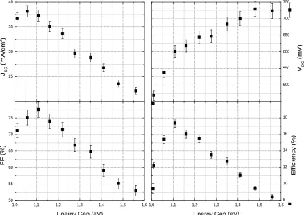
Uniform Band Gap
In order to validate the parameters in the model set-up, the dependence of the device performances on the band-gap energy was investigated considering in-itially a uniform band-gap. The main effect expected and observed by the change of GGI in the CIGS layer is the shift of the conduction band (CB) minimum [29] [30].
Current-voltage (I-V) simulations were carried out using the trap model de-scribed above. The resulting main solar cell parameters: open circuit voltage (VOC), short circuit current (JSC), fill factor (FF) and efficiency (η) are presented
in Figure 3.
The results obtained with simulations are completely in agreement with what was observed experimentally [31]. The efficiency is not rising proportionally to the increase of the band gap but it rises only in the compositional range between GGI = 0.2 and GGI = 0.3. This behaviour can be explained considering that the defect density changes with the variation of the Ga content.
3. Double Graded Band Gap and Its Optimization
When a CIGS layer is produced, it is intrinsic to observe a double-grading of the
25 30 35 40
1,0 1,1 1,2 1,3 1,4 1,5 1,6
50 55 60 65 70 75
1,0 1,1 1,2 1,3 1,4 1,5 1,6
JSC
(
m
A
/c
m
2 )
500 550 600 650 700 750
VOC
(
m
V
)
FF (
%
)
Energy Gap (eV) Energy Gap (eV)
8 10 12 14 16 18
E
ff
ici
e
n
cy (
%
[image:6.595.91.530.376.686.2])
DOI: 10.4236/msce.2018.64015 153 Journal of Materials Science and Chemical Engineering
compositional ratio in the absorber. The double grading is caused by an inade-quate inter-diffusion of the intermediate phases that results in an increase of the [Ga]/([In] + [Ga]) ratio both toward the back contact and the space charge re-gion (SCR). Therefore a typical double-grading profile is formed, which exhibits a minimum amount of Ga in the middle layer region and an increased amount toward the CIGS/Mo and the CIGS/CdS interfaces in the absorber layer. A number of studies have already demonstrated the beneficial effects of the double-grading strategy on the solar cell efficiency [8][32][33].
In order to optimise a double-grading for an enhancement of the CIGS solar cell performance we started with the study of three different grading profiles measured and reported in [16]. The different profiles, experimentally assessed by secondary ion mass spectrometry (SIMS) by Chirilă et al. [16] are shown in Fig-ure 4 (dot lines). Based on these SIMS curves the depth profiles reported in Fig-ure 4 (solid lines) were obtained and implemented in the simulation model.
In order to better study the influence of the double grading, the depth-profiles of the three samples were simplified in three separate areas: a higher front grad-ing (decreasgrad-ing band gap toward the middle of the absorber layer), a plateau characterized by a uniform band gap, and a back-graded profile that reaches a maximum and then stabilizes (Figure 4).
[image:7.595.236.514.477.669.2]The performances of the devices with the described Ga profiles (Figure 4) were analyzed by I-V curve simulations, at the temperature of 300 K with the standard AMG1.5 spectrum and considering CIGS thickness of 2 µm. The simu-lations showed the best performances for sample C (the “green” line of Ga pro-file reported in Figure 4), as it was also reported in [16]. These simulation re-sults were obtained considering the trap model for bulk defect density described in Section 2.1, which directly creates a relation between the trap concentration in
Figure 4. Ga profiles of three samples (A-C) from reference [16] showing the compositional ratio GGI along the CIGS layer depth (dot lines). Piece-wise linear Ga depth profiles (solid lines) based on [16] are implemented in the model.
0.00 0.25 0.50 0.75 1.00 1.25 1.50 1.75 2.00
0.0 0.1 0.2 0.3 0.4 0.5 0.6
G
G
I =
[G
a
]/([G
a
]+
[In
])
CIGS layer depth (µm) Model A
Model B Model C Sample A Sample B Sample C
back front
DOI: 10.4236/msce.2018.64015 154 Journal of Materials Science and Chemical Engineering
the absorber layer and the Ga content. The solar cell parameters, extracted from the simulated I-V curve and reported in Table 2 are in good agreement with the experimental results of [16].
The possible reasons for the better performance of Sample C (based on the Ga grading profiles presented in Figure 4) which are considered in the further analysis are the following:
• The front grading height (Δyf) is less pronounced for sample C (Δyf = 0.16)
than in the case of samples A (Δyf = 0.38) and B (Δyf = 0.25).
• The front grading in sample C is exactly confined to the SCR. The Ga profile
at the front of the absorber layer decreases until 1.6 μm, so considering Fig-ure 4 for an overall depth of 0.4 μm which represents the width of the space charge region, as it was confirmed by capacitance-voltage simulations. Hence, the front Ga profile does not extend beyond the space charge region. It is important to confine the front grading in this area, since a rise of Eg in the SCR will generate an additional electric field E that will work against the electric field of the p-n junction retarding the transport of electrons. In prin-ciple, this effect could be detrimental for the performances of the device. Thus, in order to avoid the deterioration of the photo-current, the front grading should be confined to the SCR where the quasi-electric field E, pro-duced by the band-gap variation, should be smaller than the field caused by the p-n junction. This will allow photo-generated electron-hole pairs to be separated without recombination avoiding a sharp decrease of the pho-to-current caused by the quasi-electric field E.
• Sample C exhibits a plateau at a CIGS layer depth which corresponds to the
region where the defects concentration approaches the minimum value (Figure 2). Therefore a lower bulk defect density is expected in this area.
3.1. Effect of Δy
fIn order to understand the effect of Δyf on the solar cell performances band
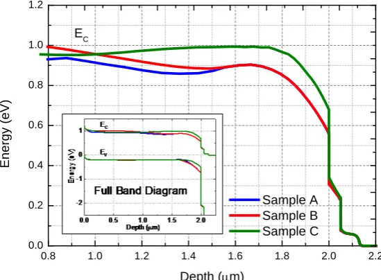
dia-gram simulations at room temperature were carried out. The results are reported in Figure 5.
Band diagram simulations show that a larger front grading height results in a more evident notch in the CB (Sample A) as it is presented in Figure 5. This notch, already visible at T = 300 K, is situated just behind the space charge re-gion. Simulations show that a larger value of Δyf results in larger barrier for
[image:8.595.206.540.656.725.2]electrons. The notch acts like a trap for electrons and its effect will be stronger at
Table 2. Solar cell main parameters of sample C, extracted from I-V curves, compared with measurement results reported in [16].
Solar cell parameters
VOC (mV) JSC (mA/cm2) FF (%) η (%)
Measured [16] 712 34.8 75.7 18.7
DOI: 10.4236/msce.2018.64015 155 Journal of Materials Science and Chemical Engineering
Figure 5. Band diagram simulations at T = 300 K for the three different Ga profiles of samples A, B and C with focus on the more prominent notch in the CB at around 1.5 μm, visible just behind the space charge region for the samples with a larger Δyf (Samples A and B).
lower temperature when the thermal energy is not sufficient for the electrons to overcome the barrier. From these results it can be concluded that a steep Ga grading profile increases the recombination probability, due to the formation of this barrier behind the space charge region. From considerations reported above, we can conclude that the double grading profile of sample C is more suitable than of samples A and B.
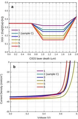
Once demonstrated and studied the reason of better performances of Sample C and assuming the possibility to control the compositional ratio in the absorber layer with high precision, we carried out several simulations considering differ-ent Ga profiles based on sample C in order to extract the most suitable double-grading profile obtaining efficient CIGS solar cell. The simulated com-positional ratios are reported in Figure 6(a) and the resulting I-V curves are shown in Figure 6(b). A summary of the solar cells parameters for the different Ga profiles are reported in Table 3.
As it can be observed from Table 3, the best solar cell efficiency is obtained for the sample 4 that presents a front grading height Δyf = 0.22, confined in the
space charge region. The plateau region for this sample is positioned at CIGS layer depth of 1.63 µm so exactly 0.37 µm of distance from the CIGS/CdS inter-face, in the area in which a minimum defects density is expected according to the trap model reported in Figure 2. This sample presents the highest values for both VOC and JSC. Due to the high thickness of the absorber layer (2 μm), the
grading at the back contact is playing a negligible role.
Preliminary simulations have also demonstrated that, in order to improve the solar cell performances, the position of the plateau in a region of minimum de-fects density is more relevant than the front grading height. Considering a fixed
0.8 1.0 1.2 1.4 1.6 1.8 2.0 2.2 0.0
0.2 0.4 0.6 0.8 1.0 1.2
E
ner
gy
(
eV
)
Depth (µm)
DOI: 10.4236/msce.2018.64015 156 Journal of Materials Science and Chemical Engineering
Figure 6. (a) Different Ga profiles implemented in the simulations in order to extract the most suitable front and back grading profiles; (b) Simulated I-V curves obtained using the different compositional ratio reported in Figure 6(a).
Table 3. Solar cells parameters for different front and double grading combinations ex-tracted from simulated I-V curves reported in Figure 6(b).
Solar cell parameters
VOC (mV) JSC (mA/cm2) FF (%) η (%) Δyf
1 707 34.75 74.75 18.4 0.11
2 (sample C) 710 35.01 75.2 18.7 0.16
3 713 35.16 75.56 18.9 0.18
4 764 37.3 75.20 21.4 0.22
5 707 36.97 73.64 19.24 0.26
6 671 36.43 72.30 17.67 0.28
Sample with uniform defects distribution at
GGI = 0.2 (Figure 3) 602 37.2 77.5 17.4 -
0.0 0.2 0.4 0.6 0.8 1.0 1.2 1.4 1.6 1.8 2.0
0.0 0.1 0.2 0.3 0.4 0.5 0.6 1
2 (sample C) 3 4 5 6 G G I = [G a ]/([G a ]+ [In ])
CIGS layer depth (µm)
a
0.0 0.2 0.4 0.6 0.8
-50 -40 -30 -20 -10 0
b
C u rre n t D e n s ity (m A /c m 2 ) Voltage (V) 12 (sample C) 3
[image:10.595.209.539.560.737.2]DOI: 10.4236/msce.2018.64015 157 Journal of Materials Science and Chemical Engineering
position for the plateau and changing just the front grading height an absolute change in the efficiency lower than 1% was observed. Simulation results for the highest performing device with uniform defect distribution at a GGI = 0.2 (see
Figure 3), which corresponds to minimum defects concentration, are reported for a comparisons in Table 3. The efficiency of the device with uniform defects distribution is shown to be lower than the efficiency of all presented devices with graded Ga profile. This behavior is mainly caused by the low VOC.
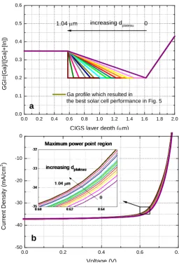
3.2. Variation of Low Ga Plateau Length
Starting from the Ga profile of sample number 4 (Figure 6(a)) which gives the best solar efficiency different lengths of the plateau were tested in order to un-derstand its relevance in the solar cell performances. The different shapes of si-mulated compositional ratios are reported in Figure 7(a).
[image:11.595.246.503.293.669.2]The simulated I-V curves obtained using the Ga profiles from Figure 7(a) are
Figure 7. (a) Ga profiles implemented in the model in order to extract the most suitable length of the plateau for high efficient CIGS solar cell; (b) Simulated I-V curves obtained using the Ga profiles reported in Figure 7(a).
0.0 0.2 0.4 0.6 0.8 1.0 1.2 1.4 1.6 1.8 2.0
0.0 0.1 0.2 0.3 0.4 0.5 0.6
a
Ga profile which resulted in
the best solar cell performance in Fig. 5
G
G
I=
[G
a
]/([G
a
]+
[In
])
CIGS layer depth (µm) 0 increasing dplateau 1.04 µm
0.0 0.2 0.4 0.6 0.8
-50 -40 -30 -20 -10 0
b
C
u
rre
n
t D
e
n
s
ity
(m
A
/c
m
2 )
DOI: 10.4236/msce.2018.64015 158 Journal of Materials Science and Chemical Engineering
presented in Figure 7(b). It can be seen that the differences in the solar cell per-formances, caused by the variation of the lengths of the plateau, are much less relevant than the front grading height. The best solar cell performance is reached for a minimum plateau length (the purple line of the Ga profile of Figure 7(a)); for higher GGI values of the plateau region the solar cell efficiencies are slightly decreasing. The changes in the solar cell efficiency values are less than 1% (21.9% for dplateau = 0, 21.1% for dplateau = 1.04 µm). It can be concluded that the
compositional ratio value at which the plateau is positioned has more impact on the cell efficiency than its length.
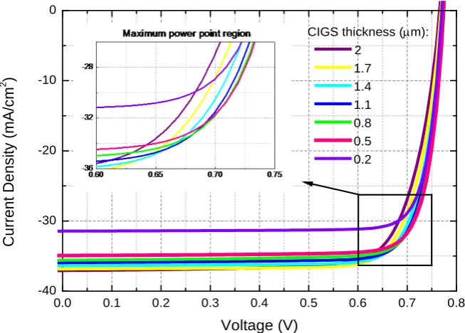
3.3. Absorber Layer Thickness Variation
Once the most suitable values and structure for the front grading height and the length and position of the plateau were established, the effect of decreased CIGS thickness on the cell performance was simulated. Thicknesses of 2, 1.7, 1.4, 1.1, 0.8, 0.5 and 0.2 µm were considered. The Ga profile which has shown the best solar cell performances in the previous simulation was used (Δyf = 0.22 and
minimum dplateau). The simulated I-V curves are reported in Figure 8.
[image:12.595.211.538.445.679.2]The best efficiency is obtained for a thickness of the absorber layer between 0.8 and 1.4 μm that provide solar cells efficiency over 22.5%, the gain in this range is also due to the beneficial effect of the grading at the back contact which becomes relevant. It can be seen that the simulated devices show almost constant high performance when an absorber layer between 0.5 - 0.8 μm is used. On the contrary a significant drop of the efficiency is observed when the CIGS thickness is further reduced. FF slightly increases when reducing the thickness of the
Figure 8. Simulated I-V curves for different thicknesses of the absorber layer, considering the Ga profile resulted in best solar cell performances reported in Figure 6. Zoom of the maximum power point region.
0.0 0.1 0.2 0.3 0.4 0.5 0.6 0.7 0.8
-40 -30 -20 -10 0
C
u
rre
n
t D
e
n
s
ity
(m
A
/c
m
2
)
Voltage (V)
CIGS thickness (µm):
2
1.7
1.4
1.1
0.8
0.5
DOI: 10.4236/msce.2018.64015 159 Journal of Materials Science and Chemical Engineering
absorber layer and VOC is almost not affected (a change less than 10 mV has been
obtained by simulations). The parameter which is the most influenced by the absorber thickness reduction is JSC, which dramatically deteriorates when
reduc-ing CIGS thickness due to reduced absorbance. The simulations results are con-firmed by the experimental studies presented in [34].
4. Conclusion
In this study, we investigated the effects of different Ga profiles on the electrical parameters of the CIGS solar cells. The aim of this work was to propose the most suitable double-grading profile in order to enhance the efficiency of the device. Our results show that an in-depth control of the front-grading is necessary in order to produce high-performing solar cell. The optimum forward double-grading needs to be confined in the SCR with a height Δyf equal to 0.22.
Higher values of Δyf bring to a deterioration of the cell performances due to the
creation of a barrier for electron just behind the space charge region. Moreover, the simulations lead to the conclusion that a good control of the position of the plateau in the Ga profile is more important that the length of the plateau itself. The plateau needs to be positioned at compositional ratio value of GGI = 0.2, in the area with the lowest defect density according to the trap model considered in the simulations. Furthermore, we showed that higher performances are reached when the CIGS thickness is reduced to 0.8 - 1.4 μm. In this thickness range de-vice efficiencies higher than 22.5% were observed. These simulations results are of considerable relevance for the material optimization of the CIGS absorber layer.
Acknowledgements
This work has been supported by the Austrian Research Promotion Agency FFG through the project SynerCIS, project No. 840706, by the European Commission FP7-NMP Programme project SolarDesign, under the grant agreement No. 310220 and also by European Community’s Framework Programme for Re-search and Innovation Horizon 2020 (2014-2020) project CABRISS under grant agreement no. 641972.
References
[1] Green, M.A., Emery, K., Hishikawa, Y., Warta, W. and Dunlop, E.D. (2017) Solar Cell Efficiency Tables (Version 51). Progress in Photovoltaics: Research and Appli-cations, 25, 668-676. https://doi.org/10.1002/pip.2909
[2] Green, M.A., Emery, K., Hishikawa, Y., Warta, W. and Dunlop E.D. (2015) Solar Cell Efficiency Tables (Version 46). Progress in Photovoltaics: Research and Appli-cations, 23, 1-9. https://doi.org/10.1002/pip.2573
[3] Niki, S., Contreras, M. Repins, I., Powalla, M., Kushiya, K., Ishizuka, S. and Matsu-bara, K. (2010) CIGS Absorbers and Processes. Progress in Photovoltaics: Research and Applications, 18, 453-466. https://doi.org/10.1002/pip.969
DOI: 10.4236/msce.2018.64015 160 Journal of Materials Science and Chemical Engineering Cu(In,Ga)Se2 Thin Film by Sputtering from Cu(In,Ga)Se2 Quaternary Target.
Progress in Natural Science: Materials, 23, 133-138.
https://doi.org/10.1016/j.pnsc.2013.02.006
[5] Lincot D., Guillemoles, J.F., Taunier, S., Guimard, D., Sicx-Kurdi, J., Chaumont, A., Roussel, O., Ramdani, O., Hubert, C., Fauvarque, J.P., Bodereau, N., Parissi, L., Panheleux, P., Fanouillere, P., Naghavi, N., Grand, P.P., Benfarah, M., Mogensen, P. and Kerrec, O. (2004) Chalcopyrite Thin Film Solar Cells by Electrodeposition. So-lar Energy, 77, 725-737. https://doi.org/10.1016/j.solener.2004.05.024
[6] Kapur, V.K., Bansal, A., Le, P. and Asensio, O.I. (2003) Non-Vacuum Processing of CuIn1-xGaxSe2 Solar Cells on Rigid and Flexible Substrates Using Nanoparticle
Pre-cursor Ink. Thin Solid Films, 431-432, 53-57.
https://doi.org/10.1016/S0040-6090(03)00253-0
[7] Lippold, G., Neumann, H. and Schindler, A. (2001) Ion Beam Assisted Deposition of Cu(In,Ga)Se2 Films for Thin Film Solar Cells. Materials Research Society Symposia Proceedings, 668, H3.9.
[8] Ramanathan, K., Contreras, M.A., Perkins, C.L., Asher, S., Hasoon, F.S., Keane, J., Young, D., Romero, M., Metzger, W., Noufi, R., Ward, J. and Duda, A. (2003) Properties of 19.2% Efficiency ZnO/CdS/CuInGaSe2 Thin-Film Solar Cells. Progress
in Photovoltaics: Research and Applications, 11, 225-230.
https://doi.org/10.1002/pip.494
[9] Gabor, A.M., Tuttle, J.R., Albin, D.S., Contreras, M.A., Noufi, R. and Hermann, A.M. (1994) High-Efficiency CuInxGa1−xSe2 Solar Cells Made from (Inx,Ga1−x)2Se3
Precursor Films. Applied Physics Letters, 65, 198-200.
https://doi.org/10.1063/1.112670
[10] Marudachalam, M., Birkmire, R.W., Hichri, H., Schultz, J.M., Swartzlander, A. and Al-Jassim, M.M. (1997) Phases, Morphology, and Diffusion in CuInx-Ga1-xSe2CuInxGa1-xSe2 Thin Films. Journal of Applied Physics, 82, 2896-2905.
https://doi.org/10.1063/1.366122
[11] Pettersson, J., Platzer-Björkman, C., Zimmermann, U. and Edoff, M. (2011) Base-line Model of Graded-Absorber Cu(In,Ga)Se2 Solar Cells Applied to Cells with
Zn1-XMgxO Buffer Layers. Thin Solid Films, 519, 7476-7480.
https://doi.org/10.1016/j.tsf.2010.12.141
[12] Lundberg, O., Edoff, M. and Stolt, L. (2005) The Effect of Ga-Grading in CIGS Thin Film Solar Cells. Thin Solid Films, 480, 520-525.
https://doi.org/10.1016/j.tsf.2004.11.080
[13] Lundberg, O., Bodegård, M., Malmström, J. and Stolt, L. (2003) Influence of the Cu(In,Ga)Se2 Thickness and Ga Grading on Solar Cell Performance. Progress in
Photovoltaics: Research and Applications, 11, 77. https://doi.org/10.1002/pip.462
[14] Burgelman, M., Nollet, P. and Degrave, S. (2000) Modelling Polycrystalline Semi-conductor Solar Cells. Thin Solid Films, 361-362, 527-532.
https://doi.org/10.1016/S0040-6090(99)00825-1
[15] Ouédraogo, S., Zougmoré, F. and Ndjaka, J.M. (2013) Numerical Analysis of Cop-per-Indium-Gallium-Diselenide-Based Solar Cells by SCAPS-1D. International Journal of Photoenergy, 2013, 421076. https://doi.org/10.1155/2013/421076
[16] Chirilă, A., Buecheler, S., Pianezzi, F., Bloesch, P., Gretener, C., Uhl, A.R., Fella, C., Kranz, L., Perrenoud, J., Seyrling, S., Verma, R., Nishiwaki, S., Romanyuk, Y.E., Bilger, G. and Tiwari, A.N. (2011) Highly Efficient Cu(In,Ga)Se2 Solar Cells Grown
on Flexible Polymer Films. Nature Materials,10, 857-861.
DOI: 10.4236/msce.2018.64015 161 Journal of Materials Science and Chemical Engineering [17] Jackson, P., Hariskos, D., Lotter, E., Paetel, S., Wuerz, R., Menner, R., Wischmann, W. and Powalla, M. (2011) New World Record Efficiency for Cu(In,Ga)Se2
Thin-Film Solar Cells beyond 20%. Progress in Photovoltaics: Research and Appli-cations,19, 894-897. https://doi.org/10.1002/pip.1078
[18] Hashimoto, Y., Kohara, N., Negami, T., Nishitani, N. and Wada, T. (1988) Chemi-cal Bath Deposition of Cds Buffer Layer for GIGS Solar Cells. Solar Energy Mate-rials and Solar Cells,50, 71-77.
[19] Minemoto, T., Matsui, T., Takakura, H., Hamakawa, T., Negami, T., Hashimoto, Y., Uenoyama, T. and Kitagawa, M. (2001) Theoretical Analysis of the Effect of Con-duction Band Offset of Window/CIS Layers on Performance of CIS Solar Cells us-ing Device Simulation. Solar Energy Materials and Solar Cells,67, 83-88.
https://doi.org/10.1016/S0927-0248(00)00266-X
[20] Parisi, A., Pernice, R., Rocca, V., Curcio, L., Stivala, S., Cino, A.C., Cipriani, G., Di Dio, V., Galluzzo, G.R., Miceli, R. and Busacca, A.C. (2015) Graded Carrier Con-centration Absorber Profile for High Efficiency CIGS Solar Cells. International Journal of Photoenergy,2015, Article ID: 410549.
https://doi.org/10.1155/2015/410549
[21] Pettersson, J., Torndahl, T., Platzer-Bjorkman, C., Hultqvist, A. and Edoff, M. (2013) The Influence of Absorber Thickness on Cu(In,Ga)Se2 Solar Cells with
Dif-ferent Buffer Layers. IEEE Journal of Photovoltaics,3, 1376.
[22] Wadaa, T., Kohara, N., Nishiwaki, S. and Negami, T. (2001) Characterization of the Cu(In,Ga)Se2/Mo Interface in CIGS Solar Cells. Thin Solid Films,387, 118-122.
[23] Kuo, S.-Y., Hsieh, M.-Y., Hsieh, D.-H. and Kuo, H.-C. (2014) Device Modeling of the Performance of Cu(In,Ga)Se2 Solar Cells with V-Shaped Bandgap Profiles.
In-ternational Journal of Photoenergy,2014, Article ID: 186579.
https://doi.org/10.1155/2014/186579
[24] Schroeder, D.J., Hernandez, J.L. and Rockett, A.A. (1997) Point Defects and Hole Transport in Epitaxial CuIn1-xGaxSe2. Proceedings of the 11th International Con-ference on Ternary and Multinary Compounds, Salford, 8-12 September 1997, 749-752.
[25] Song, S.H., Nagaich, K., Aydil, E.S., Feist, R., Haley, R. and Campbell, S.A. (2010) Structure Optimization for a High Efficiency CIGS Solar Cell. 35th IEEE Photovol-taic Specialists Conference, Honolulu, 20-25 June 2010, 2488-2492.
[26] Song, J., Li, S.S., Huang, C.H., Crisalle, O.D. and Anderson, T.J. (2004) Device Modeling and Simulation of the Performance of Cu(In1−x,Gax)Se2 Solar Cells.
Sol-id-State Electronics,48, 73-79.
[27] Paulson, P.D., Birkmire, R.W. and Shafarman, W.N. (2003) Optical Characteriza-tion of CuIn1−xGaxSe2 Alloy Thin Films by Spectroscopic Ellipsometry. Journal of
Applied Physics,94, 879-888. https://doi.org/10.1063/1.1581345
[28] Hanna, G., Jasenek, A., Rau, U. and Schock, H.W. (2001) High Quality Baseline for High Efficiency, Cu(In1−x,Gax)Se2 Solar Cells. Thin Solid Films, 387, 71-72.
[29] Wei, S.H. and Zunger, A. (1995) Band Offsets and Optical Bowings of Chalcopyrites and Zn-Based II-VI Alloys. Journal of Applied Physics,78, 3846.
https://doi.org/10.1063/1.359901
[30] Gorji, N.E., Perez, M.D., Reggiani, U. and Sandrolini, L. (2012) A New Approach to Valence and Conduction Band Grading in CIGS Thin Film Solar Cells. Internation-al JournInternation-al of Engineering & Technology,4, 573-576.
DOI: 10.4236/msce.2018.64015 162 Journal of Materials Science and Chemical Engineering (1997) Prospects of Wide-Gap Chalcopyrites for Thin Film Photovoltaic Modules Solar. Energy Materials and Solar Cells, 49, 227-237.
[32] Dullweber, T., Rau, U., Contreras, M.A., Noufi, R. and Schock, H.-W. (2000) Pho-togeneration and Carrier Recombination in Graded Gap Cu(In,Ga)Se2 Solar Cells.
IEEE Transactions on Electron Devices, 47, 2249-2254.
[33] Gloeckler, M. and Sites, J.R. (2005) Band-Gap Grading in Cu(In,Ga)Se2 Solar Cells.
Journal of Physics and Chemistry of Solids,66, 1891-1894.
https://doi.org/10.1016/j.jpcs.2005.09.087
[34] Lundberg, O., Bodegaerd, M., Malmstroem, J. and Stolt, L. (2003) Influence of the Cu(In,Ga)Se2 Thickness and Ga Grading on Solar Cell Performance. Progress in
![Figure 2. Variation of the traps (defects) concentration with Ga composition implemented in the model in order to model bulk de-fects in the absorber layer [25]](https://thumb-us.123doks.com/thumbv2/123dok_us/9294531.426554/5.595.249.502.444.655/figure-variation-traps-defects-concentration-composition-implemented-absorber.webp)
![Figure 4. Ga profiles of three samples (A-C) from reference [16] showing the compositional ratio GGI along the CIGS layer depth (dot lines)](https://thumb-us.123doks.com/thumbv2/123dok_us/9294531.426554/7.595.236.514.477.669/figure-profiles-samples-reference-showing-compositional-ratio-cigs.webp)
![Table 2. Solar cell main parameters of sample C, extracted from I-V curves, compared with measurement results reported in [16]](https://thumb-us.123doks.com/thumbv2/123dok_us/9294531.426554/8.595.206.540.656.725/table-solar-parameters-extracted-compared-measurement-results-reported.webp)