Controller Implementation for PV Interconnection Based
Three-Phase UPS Systems Operating Under Highly
Nonlinear Loads
1
P. Muni Sravani,
2D
. Srilatha
,
3M. Bala Subba Reddy
1M.Tech, Scholar,
2Associate Professor,
3Associate Professor& H.O.D
Dept of EEE, Prakasam Engineering College, Kandukur.
Abstract—This paper presents the design of a PV
interconnection system based three-phase uninterruptible power supply (UPS) systems that are operating under highly nonlinear loads. The classical high-performance sinusoidal pulse width modulation (SPWM) control method is quite effective in controlling the RMS magnitude of the UPS output voltages. However, it is not good enough in compensating the harmonics and the distortion caused specifically by the nonlinear currents drawn by the rectifier loads. This study proposes a new design strategy that overcomes the limitations of the classical RMS control. It adds inner loops to the closed-loop control system. Simulink is used to analyze, develop, and design the controller using the state-space model of the inverter. By the implementation of PV system based inverter we are analyzing the efficiency of proposed model of SPWM. Simulation performance is evaluated for a three-phase 10 kVA transformer isolated UPS under all types of load conditions. In conclusion, the simulation results demonstrate that the controller successfully achieves the steady-state RMS voltage regulation specifications as well as the total harmonic distortion and the dynamic response requirements of major UPS standards.
Index Terms— PV system, Inverter, nonlinear
load, sinusoidal pulse width modulation (PWM) control, uninterruptible power supply (UPS).
I. INTRODUCTION
The increased use of rectifiers in critical loads employed by the information technologies, and medical and
military equipment mandate the design of uninterruptible
power supplies (UPS) with high-quality outputs [1]–[3]. The highly nonlinear currents drawn especially by high-power single-phase rectifier loads greatly distort the UPS outputs. The distorted UPS voltages cause generation of
low dc voltage at the output of the rectifier loads, which causes high current flow, increased power losses, and possibly the malfunction of the critical load or the UPS.
The distortion is resulted mainly by the voltage drop
across the inductive element of the LC filter due to the non
sinusoidal current at the output of the inverter [4]–[6]. In a UPS system the inverter is responsible for synthesizing sinusoidal voltages from a dc source through the pulse width modulation (PWM) of the dc voltage, for the selected switching frequency and the power level, an optimum filter with a smallest inductance can be designed, but the distortion cannot be completely avoided, and the regulations and the customer specifications may not be satisfied.
However, the classical sinusoidal PWM (SPWM) method is still preferred by many manufacturers because of its implementation simplicity, easy tuning even under load, flexibility, and most importantly the advantages of controlling each phase independently. Although the classical SPWM method is quite effective in controlling the RMS magnitude of the UPS output voltages, it is not good enough in compensating the harmonics and the distortion caused specifically by the nonlinear loads [8], [9].
It uses a droop strategy to cancel the power transfer at the harmonic frequencies and therefore eliminate the distortion at the output voltage caused by the voltage drop across the inverter impedance due to the harmonic currents.. However, the significance of the proposed multiloop controller compared to other methods is as Follows:
1) The execution time is less and allows higher
switching frequencies. The complex control algorithms take longer execution times and may limit the upper boundary of the switching frequency where you have actually some allowance for higher switching frequency operation [36]. Examples to the complex controllers are the
repetitive, predictive, and harmonic droop
controllers.
2) The cost is low. Some control algorithms require
precise floating point calculations either because they depend on a precise model or they use frequency-dependent sensitive controller gains. In brief, the precision dictates use of high-performance floating point expensive microcontrollers.
3) The easy tuning even under load: Some are robu st to this kind of tuning and some may not. This feature is preferred by some manufacturers. The
easy tuning of the proposed method under load is verified during the experimental studies.
4) The flexibility: It means that you can modify your controller and optimize it according to the customer specifications at the time of installation or later in use. The optimization may include obtaining the lowest THD or the best tracking of the RMS value or the fastest dynamic response. So, the controller should be flexible anytime to do any of the aforementioned optimizations without significantly affecting the others. We have also verified this feature experimentally.
5) The scalability: It means that the controller is easy to design and tunable for any power level.
Fig.1. Single-line diagram of a typical three-phase four-wire transformer isolated UPS system.
II. SYSTEM DESCRIPTION
The single-line diagram of a typical three-phase four-wire transformer isolated UPS system is
inverter (VSI) creates balanced three-phase sinusoidal voltages across the load terminals at the
utilization frequency and magnitude. The LC
low-pass filter removes the harmonics generated by the PWM switching. The Δ-winding of the transformer blocks the third harmonic currents at the inverter
side, and the zigzag winding provides a neutral point and zero phase difference for the load-side voltages. The load can be a three-phase or a single phase load ranging from linear to nonlinear load with a crest factor up to 3. The UPS uses a digital controller implemented in a fixed-point DSP controller.
III. ANALYSIS OF THE UPS INVERTER POWER STAGE
This section obtains the state-space model of the inverter stage of a three-phase UPS in order to design the controller for the inverter. The developed model is also used to study the controller performance for the lowest THD of the output voltage while maintaining the stability and a good dynamic response under all load conditions. The model is developed based on the circuit schematic given in Fig. 2.
As shown in Fig. 2, an insulated gate bipolar transistor (IGBT)-based three-phase inverter is used to produce pulse-width modulated voltages across the terminals labeled as 1, 2, and 3. Moreover, L is the external filter inductor used to reduce ripple at the line current, Llk1 is the primary side leakage, and Lμ is the magnetizing inductance of the transformer; then L_lk2 is the secondary side leakage inductance, C_is
the filter capacitor, and finally R_ is the load
resistance (the prime symbol represents the parameters referred to the Δ-side of the transformer). Writing the voltage equations at the Δ-side of the transformer yields the following sets of equations for the line-to-line voltages across the inverter terminals, (1) as shown at the bottom of the page. Similarly, writing the current equations yields the following sets of equations for the derivative of the transformer secondary currents:
Likewise, the following sets of equations are obtained for the derivative of the referred output voltages based on the output parameters:
In addition, the inverter terminal voltages given in (1) can also be written in terms of the moving average of the switching functions, the modulation ratio ma , and the dc bus voltage Vdc. The
moving average of the switching functions is actually equal to the control signals that are applied to the comparators to generate the PWM signals for the inverter switches.
Consequently, the following sets of
Fig.2.UPS inverter stage including the Δ-zigzag transformer equivalent circuit and the resistive load.
Where ucont abc represents the control signals produced
by the controller for each inverter leg. The modulation ratio ma is equal to the peak of the control signal _U cont divided by the peak of the triangular carrier waveform
_Vtri . Although the parameter _V tri is always constant;
Vdc may be changing depending on the grid conditions.
It is relatively constant when grid is okay due to the controlled rectifier, but it is varying when grid is gone and the inverter works from the battery pack. These conditions are studied during the performance testing of the controller.
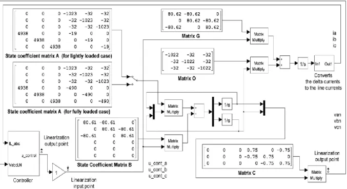
Deriving the derivative of the delta winding currents from (1) first, and then using them in (2), and also using (4) for the inverter terminal voltages, the following sets of the state-space equations are obtained. These equations are based on selecting the referred transformer secondary currents and the output voltages as the state variables and the control signals as the inputs
Defining the parameters L1, L2 , and L3 as given next
allows compact entries of the matrices A and B
TABLE I
MAJOR UPS DESIGN SPECIFICATIONS
We also need to determine the current through the external filter inductors at the inverter output (ia, ib ,
and ic ) since they are used as the feedback in the
closed-loop control system. These currents are the transformer delta winding currents converted into the line currents. The following sets of equations yield the derivatives of the delta winding currents:
The entries Oij and Gij in the aforementioned matrices
are found using
The state-space model of the proposed inverter design is given in the next section after the design parameters are determined based on the given specifications.
IV. DESIGN OF THE INVERTER POWER STAGE
The specifications used for the design of the inverter power stage are given in Table I. The design process initially assumed a resistive load and used the classical methods and the rule of thumbs suggested in the power electronics literature. However, this design did not give a good performance under nonlinear loads. Then, it is improved via simulation studies until the desired performance is achieved for all load cases.
The improvements included determination of the proper dc bus voltage, switching frequency, transformer parameters, and the element values of the LC filter.
Our preliminary design goal is to maintain the THD always below 4% under the worst case. The worst case is defined as the instant dc bus voltage is at the minimum while the UPS is delivering the rated nonlinear load.
The simulation studies have shown that if the controller goes into over modulation region, the THD specification cannot be satisfied. Therefore, the nominal dc bus voltage is maintained at 405 V when grid is okay and it is allowed to reduce down to 300 V when grid is gone and the UPS operates from the battery pack. One string of the battery pack consists of 30 pieces of 12 V lead-acid batteries connected in series.
Simulation studies, it has been realized that the output impedance of an inverter plays an important role in reducing the THD of the output voltage. And the results show that the THD of the voltage can be improved if the output impedance is reduced [5] or the impedance is modified to become even more capacitive in nature [6]. Our approach to design the LC filter is to start first with finding practically the smallest inductance value, and then finding the capacitance value based on filtering requirement of the switching frequency ripple at the output voltage. Generally, the inductance is selected based on the current ripple, size, and dynamic response criteria. Since we want the smallest inductance, we base our inductor design on the ripple requirement. The current through the inductor also flows through the IGBTs of the three-phase inverter at every switching cycle. So, based on our experience, allowing 30% ripple at the current is considered a good compromise between the size and the efficiency requirements. More than 30% ripple allows smaller inductance but causes larger turn-off switching losses.
Hence, the inductance is calculated based on the forementioned ripple specification, and then the capacitance value is calculated in such a way
that the LC filters produces 30 dB attenuation at the
the inverter side and the capacitor is 120 μF placed at the load side. The calculated inductance yields around 30% current ripple at the inverter line currents at the full linear load and a corner frequency of 352 Hz for
the LC filter. As shown in Fig. 3, an external inductor
equal to 30μH is added at each line to arrive at the required filter inductance value. Finally, the test loads are designed as three different Y connected loads: the first one represents a linear light load at 338 W, the second one is the linear load at 8.5 kW, and the last one is the nonlinear rectifier load at 10 kVA. The nonlinear load, which consists of three full-bridge rectifiers connected between each phase and the neutral. The rectifier load resistor is selected as 33 Ω
to dissipate total 6.6 kW equal to 66% of the rated three-phase output power, and the series input resistor is selected as 0.58 Ω to dissipate total 400 W equal to 4% of the rated output power. Additionally, the selected rectifier parameters generate a current waveform with a crest factor of 3 when tested with good mains voltages. The value of crest is important since the specification of products requested by many customers today require the UPS to handle loads up to 3 crest factor while allowing a THD no more than 5%.Finally, the schematic of the inverter with the parameter values optimized for all load conditions is shown in Fig. 3.
Fig.3. PLECS model of the designed inverter power stage including delta–zigzag transformer, the LC filter, the
measurements, and the linear and nonlinear loads.
V. STATE-SPACE MODEL OF THE INVERTER POWER STAGE
The state-space model of the plant (three-phase inverter) is needed to develop and test the controller performance So, using L = 30 μH, Lμ = 1 H, Llk1 = 820 μH, L_ lk2 = 100 μH, C_ = 202 μF, Vdc = 405 V, Vtri = 2487, R_ = 10 Ω for full load and R_ = 255 Ω for the light load case in (5) through (13), the
state-space model of the plant is obtained as shown in Fig. 4. The peak of the carrier waveform is obtained based on the type of the selected DSP and the switching frequency. The details of the controller are discussed in the next section.
VI.
C
ONTROLLERD
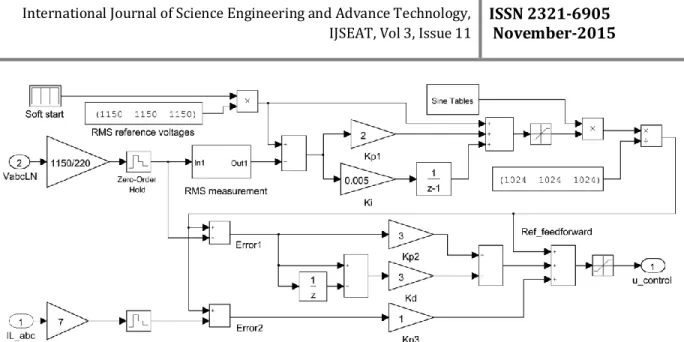
ESIGNon the multiloop SPWM method as shown in Fig. 5, which is also shown as a block in Fig. 4. The controller topology is very similar to the classical state-feedback multiloop controllers [8], [9], except that all the loops are combined (instead of cascade connection) before they are applied to the PWM generator. This feature basically adds the relative benefits of each loop and creates a more effective multiloop strategy. In order to facilitate the understanding of the proposed controller, the reasoning behind the selected control topology can be explained as follows.
The control system shown in Fig. 5 consists of one outer voltage loop and three inner loops. The outer loop is the main voltage loop, which regulates the fundamental frequency component of the output voltage and its steady-state RMS value using a PI compensator; for that reason, it has slower dynamics. The first of the inner loops is the voltage reference feedforward loop which provides fast transient response but less benefit to the compensation of the harmonic distortions. The second inner loop is the
voltage loop where the measured ac output voltages are instantaneously compared to the reference ac voltages created by the main loop and the error (Error1) is found; then the loop is compensated using a PD controller.
This loop is responsible for correcting the phase shift and improving the waveform quality of the output voltages. The simulation results confirm that the gain Kp2 controls the THD of the voltages effectively and improves the waveform quality. The dynamic characteristic of this loop is relatively fast since there is no integrator. Actually, the fast dynamic with high gain is desired since it generates the corrective control actions to compensate for the distortion caused by the nonlinear currents, but this feature easily pushes the system into instability. One solution to this problem is to add a derivative control; however, it provides a minor help to stabilizing the system. The more effective solution is to add an ac current inner loop which provides the feedback about the voltage drop across the inductive
Fig.5. Simulink model of the proposed multiloop controller.
element of the LC filter, which makes the part of the
compensation against the harmonic distortions at the voltage. In this loop, the measured inductor currents are instantaneously compared to the reference currents created by the main loop and the resulted error (Error2) is combined to the main control output after it is multiplied by the gain Kp3, as shown in Fig. 5. Our studies have shown that the ac current loop with the gain Kp3 stabilizes the control system effectively. In addition, the inductor currents that are measured for the closed-loop control are also used for overload protection and current limiting purposes. So, the cost of the current transformers is justified in this design.
The advantage of the multiloop control system proposed here is that the loops can be optimized for the best performance relatively independent of each other. For example, the outer voltage loop is tuned first for the best voltage regulation, and then the inner loops can be optimized relatively independently for the best THD of the output voltage while effectively managing and maintaining the stability. The controller parameters are determined as follows. Based on the steady-state
voltage regulation and transient response
specifications given in Table I, first the gains of the main voltage loop are determined as Kp1 = 2 and Ki = 0.05, as shown in Fig. 5. Then, the Kp2 = 3 is determined for the practical lowest THD while Kd and Kp3 are adjusted to maintain a stable operation. The proper gains for Kd and Kp3 are obtained using the control design tool for the lightly loaded case in
the model shown in Fig. 4. The lightly loaded case is the worst case in terms of the stability. Fig. 6 shows the results of the step response analysis and also illustrates the steps of the process how the controller parameters are determined
Fig. 6. Step response analysis of the closed-loop control system: (a) for Kp2 = 3, Kd = 0, and Kp3 = 0;
(b) for Kp2 = 3, Kd = 3, Kp3 = 0 (blue), Kp3 = 0.75 (green), and Kp3 = 1.0 (red).
Fig. 6(a). On the other hand, the derivative control where Kp2 = 3, Kd = 3, and Kp3 = 0 stabilizes the system, but not very effectively [the blue waveform in Fig. 6(b)]. However, a more effective stable operation is obtained when the third loop (the inner ac current loop) is activated. Fig. 6(b) shows the results for Kp2 = 3, Kd = 3, and Kp3 = 0.75 as the green waveform, and for Kp2 = 3, Kd = 3, and Kp3 = 1 as the red waveform. Consequently.
The high switching frequency allows a larger voltage loop bandwidth which enables the
controller to produce corrective actions to
compensate for the fast changing oscillations at the
voltage waveform effectively. Therefore, the
switching frequency should be optimized based on the acceptable THD versus the switching losses and the efficiency. Based on the simulation results, it is found that 10.05 KHz is the optimum switching frequency for the given application (10 kVA three-phase UPS using the PWM switching method).
VII. SIMULATION RESULTS
Proposed Multiloop Controller
The simulations are done in the
MATLAB/Simulink environment using the Simulink and PLECS model of the inverter and the controller as shown in Fig. 8. The results are evaluated based on steady-state error, transient response, and the THD of the output voltage. Fig. 9 shows the RMS value and the percent THD of the output voltage versus three different loads. According to Fig. 9, when the linear load at 8.5 kW is applied, the controller achieves 0.3% THD, and similarly when the nonlinear load at 10 kVA is applied, the controller achieves 3.1% THD. In addition, the RMS voltages are very well regulated at 220 V for each phase with an excellent transient response for the linear load but a fair response for the nonlinear load case. The transient response from no-load to the rated nonlinear load is oscillatory and it takes 1.1 s; however, the maximum
fluctuation in the RMS voltage is less than •}10% of
the nominal (198–242 V).We consider this as an expected behavior for the nonlinear load case since the capacitor of the rectifier is made fairly large to get the desired crest in current; additionally, it is all empty before the load is applied. At the instant, the
rectifier loads are switched in, a very large inrush current flows into these capacitors. So, it is this current that causes the oscillatory behavior. As mentioned before, the nonlinear load is a full-bridge diode rectifier load
Fig.7. Proposed multiloop inverter controller implemented in the
The simulated load consists of a light load, the linear full load, and the nonlinear full load. placed between each phase and the neutral as shown in Fig. 3.
Fig.8. Simulink model of the inverter system.
Fig.9. RMS fluctuations (top trace) and the profile of the percent THD of the output voltages (second trace)
versus the load delivered by the inverter (bottom trace).
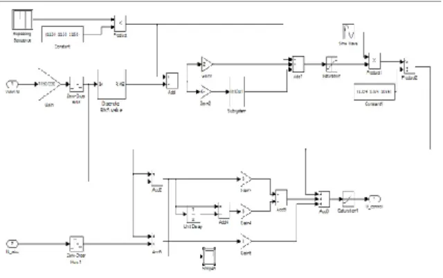
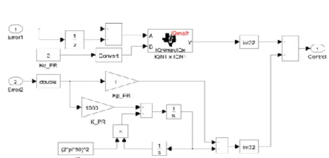
Fig.10. Inner loops of the control system: the PR controller is combined with the derivative controller.
Fig.11. Inner loops of the control system: the PR controller is combined into the proposed multiloop
controller.
Fig.12.three-phase controlled output voltages
Fig.13.Three-Phase Output Voltages (Upper) And The Load Currents (Down) And Control Voltages
(Middle)
A UPS system rated at 10 kVA, 50 Hz, 380 V was built and tested to evaluate the performance of the controller and the design. The implemented system uses the component values given in the PLECS simulation model of the converter shown in Fig. 3 (in Section IV) for the inverter part and the values given in Fig. 7 (in Section VI) for the controller part.
In Fig. 12, we compare the results of the multiloop design against the single-loop (only the RMS control) design in order to demonstrate the performance of the proposed multiloop controller. Fig. 13 compares the measured three-phase output voltages and the current of one phase for two loading conditions: the linear full load and the nonlinear full load. Fig. 12 and 13 show the results when only the RMS control is used (single-loop), for this case the control achieves 1.96% THD for the linear and 9.68% THD for the nonlinear load. It is clear that the RMS control alone cannot achieve an acceptable THD under nonlinear loading at the rated UPS output power.
The waveforms in Fig. 12 show the results when the proposed multiloop controller is used for the same loading conditions. In this case, the controller achieves 1.11% THD for the linear load and 3.8% THD for the nonlinear load. The crest factor of the current in Fig. 13 is measured as 2.8.
VIII. SIMULINK RESULTS OF PV BASED INVERTER
Fig.15.PV Simulink Model
Fig.16.THD of Output Voltage
Fig.17.RMS Value of Output Voltage
Fig.18.The Load Delivered By The Inverter Consists Of A Light Load, The Linear Full Load, And The
Nonlinear Full Load.
Fig.19.Inverter Input Reference Currents
Fig.20.Inverter Output Currents
IX. CONCLUSION
This paper presents the analysis and design of a high performance SPWM controller for three-phase pv interconnected UPS systems powering highly nonlinear loads. Although the classical SPWM method is very successful in controlling the RMS magnitude of the UPS output voltages, it cannot effectively compensate for the harmonics and the distortion caused by the nonlinear currents drawn by the rectifier loads. Therefore, this paper proposes a new strategy with a new design that overcomes the limitations of the classical RMS control. It adds inner loops to the closed loop control system effectively that enables successful reduction of harmonics and compensation of distortion at the voltages.
REFERENCES
[1] Uninterruptible power systems (UPS)—Part 3: Method of specifying the performance and test requirements, First Edition 1999-03, International Standard IEC 62040-3.
[2] F. Botter´on and H. Pinheiro, ―A three-phase UPS that complies with the standard IEC 62040-3,‖ IEEE Trans. Ind. Electron., vol. 54, no. 4, pp. 2120–2136, Aug. 2007.
[3] S. Jiang, D. Cao, Y. Li, J. Liu, and F. Z. Peng, ―Low THD, fast transient, and cost-effective synchronous-frame repetitive controller for three-phase UPS inverters,‖ IEEE Trans. Power Electron., vol. 27, no. 6, pp. 2294– 3005, 2012.
[4] U. Borup, P. N. Enjeti, and F. Blaabjerg, ―A new space-vector-based control method for UPS systems powering nonlinear and unbalanced loads,‖ IEEE Trans. Industry Appl., vol. 37, no. 6, pp. 1864–1870, Nov./Dec. 2001.
[5] Q.-C. Zhong, F. Blaabjerg, J. Guerrero, and T. Hornik, ―Reduction of voltage harmonics for parallel-operated inverters equipped with a robust droop controller,‖ in Proc. IEEE Energy Convers. Congr. Expo., Phoenix, AZ, 2011, pp. 473–478. [6] Q.-C. Zhong and Y. Zeng, ―Can the output impedance of an inverter be designed capacitive?‖ in Proc. 37th Annu. IEEE Conf. Ind. Electron., 2011, pp. 1220–1225.
[7] P.Mattavelli, ―Synchronous-fame harmonic control for high-performance AC power supplies,‖ IEEE Trans. Ind. Appl., vol. 37, no. 3, pp. 864–872, May/Jun. 2001.
[8] N. M. Abdel-Rahim and J. E. Quaicoe, ―Analysis and design of a multiple feedback loop control strategy for single-phase voltage-source UPS inverters,‖ IEEE Trans. Power Electron., vol. 11, no. 4, pp. 532–541, Jul. 1996.
[9] M. J. Ryan, W. E. Brumsickle, and R. D. Lorenz, ―Control topology options for single-phase UPS inverters,‖ IEEE Trans. Ind. Appl., vol. 33, no. 2, pp. 493–501, Mar./Apr. 1997.
[10] F. Botter´on, H. Pinheiro, H. A. Grundling, and J. R. P. H. L. Hey, ―Digital voltage and current controllers for three-phase PWM inverter for UPS applications,‖ in Proc. 36th Annu. Meeting IEEE Ind.
Appl., Chicago, IL, Sep./Oct. 2001, vol. 4, pp. 2667– 2674.
[11] P. C. Loh, M. J. Newman, D. N. Zmood, and D. G. Holmes, ―A comparative analysis of multiloop voltage regulation strategies for single and three-phase UPS systems,‖ IEEE Trans. Power Electron., vol. 18, no. 5, pp. 1176–1185, Sep. 2003.
[12] E. Kim, J. Kwon, J. Park, and B. Kwon, ―Practical control implementation of a three-to single-phase online UPS,‖ IEEE Trans. Ind. Electron., vol. 55, no. 8, pp. 2933–2942, Aug. 2008. [13] T. Kawabata, T. Miyashita, and Y. Yamamoto, ―Dead beat control of three phase PWM inverter,‖ IEEE Trans. Power Electron., vol. 5, no. 1, pp. 21– 28, Jan. 1990.
[14] Y.-Y. Tzou, R.-S. Ou, S.-L. Jung, and M.-Y. Chang, ―High-performance programmable AC power source with low harmonic distortion using DSP based repetitive control technique,‖ IEEE Trans. Power Electron., vol. 12, no. 4, pp. 715–725, Jul. 1997.
PERAM.MUNI SRAVANI currently pursuing her
M.Tech in power electronics in prakasam
engineering college, kandukur, andra pradesh, india affiliated to jntu university, kakinada. She has done his B.Tech degree from krishna chaitanya institute of technology and sciences, affiliated to jnt university, kakinada, andhra pradesh, India and her fields of interest include power electronic drives and renewable energy sources and advanced controllers.
D. SRILATHA presently working as Assistant professor in prakasam engineering college, kandukur, andhra pradesh, India. Pursuing her Ph.D from jnt university, kakinada. Her fields of interest include non conventional energy sources, advanced control techniques and electrical drives.