Effect of HNO3 Concentration on Etch Rate and Structure of Si Wafer Etched
in the Mixture of HF and HNO3 Solutions
F. Nurhaziqah K1, C. K. Sheng2∗, K. A. M. Amin2, M. I. N. Isa2, M. F. Hassan2, E. A. G. E. Ali2, K. H. Kamarudin2 and R. Aarif1
1Universiti Malaysia Terengganu, School of Ocean Engineering,
21030 Kuala Nerus, Terengganu, Malaysia.
2Advanced Nano Materials (ANoMa) Research Group,
Universiti Malaysia Terengganu, School of Fundamental Science,
21030 Kuala Nerus, Terengganu, Malaysia.
The new microelectronic products require the silicon (Si) wafer to be thinned to less than 150µm in thickness. Residual defect on the wafer surface that leads to wafer breakage with a rough surface still be produced by mechanical grinding. Thus, chemical etching method is essentially applied to produce a reliable thin wafer with smooth surface of desired thickness. In this work, we studied the wet chemical etching effect of different HNO3concentrations on
total thickness and weight loss, etch rate, morphological and structural properties of Si wafer in the mixtures of HNO3 and HF. The results showed that the total thickness and weight
loss increases with the increasing of HNO3 concentration and etching time. Higher HNO3
concentration causes higher etch rate, and the etch rate decreases at prolonged etching time. A smoother and clearer homogeneous Si surface image was observed by optical microscope as the etching time and HNO3 concentration increase. XRD analysis shows that the intensity
of etched Si wafer is higher than the pure one, which might indicate the smoother surface formation after etching. The findings of present study can be valuably referred to produce a reliable and desired Si thin wafer which is crucial in integrated circuit fabrication.
Keywords: etch rate, silicon, nitric acid, structure, microscope
I. INTRODUCTION
Thin wafers have become a basic need for a wide variety of new microelectronic products. These include power devices discrete semicon-ductors, optoelectronic components and inte-grated circuits for Radio Frequency Identifica-tion (RFID) systems. New concepts in
micro-∗
Corresponding author:[email protected]
the damage layer that is created by the coarse grinding step. However, there still remains a de-fect band near the wafer surface. The thickness of this defect zone is dependent upon the grind-ing conditions. The residual defects can cause stress in the thinned wafer that leads to addi-tional bow and can result wafer breakage. The most cost effective process is wet etching. Wafer that have been thinned using a final wet etch process on the backside will have less stress com-pared with mechanical grinding. Wafer breakage will be reduced and after dicing the chips, it will have fewer cracks and chip-outs [1]-[4]
The new microelectronic products require wafer to be thinned at the desired thickness. Residual defect on the wafer surface that leads to wafer breakage with a rough surface still pro-duced by mechanical grinding. Etching process is applied in this study to produce a reliable thin wafer with smooth surface of desire thick-ness. Abdur-Rahmanet al. (2017) has reported the influence of IPA concentration and the etch-ing time on the pyramidal surface structures on etched mc-Si in alkaline solutions [5].Narasimha Rao et al. (2017) has studied the etching be-haviour of Si in 20 wt% KOH with addition of hydroxylamine for the fabrication of bulk micro-machined MEMS, in which the etch rate and un-dercutting are improved significantly [6]. High etch rate is very useful to achieve larger etch depth in less time in comparison to common etchant.
In the manufacturing company, high etch rate
is demanded to increase the productivity that eventually reduces the cost of end product. In this study, we investigated the isotropic wet etching effect of HNO3 concentration on total
thickness and weight loss, etch rate, morpho-logical and structural properties of Si wafer in the mixtures of HF and different HNO3
con-centrations. The total thickness and weight loss percentage were measured using gravimetric method, the morphological image was obtained by optical microscope and the crystalline struc-ture was characterized by XRD
II. MATERIALS AND METHODS
The chemicals used are HNO3 (Merck Co.),
wafers were rinsed in distilled water and further dried in air
The chemical consists of different concentra-tions of etchant mixture which are constant con-centration of HF with different concon-centrations of HNO3. In this study, three different etchant
concentrations were used to study the effect of chemical etching on Si wafer, in which 20 wt%, 23 wt% and 26 wt% HNO3 etchant
concentra-tions were mixed with 48 wt% HF etchant con-centration for each Si wafer. Therefore, there are three different sets of etchant concentration mixture: HF 48 wt% / HNO3 20 wt%, HF 48 wt% / HNO3 23 wt%, and HF 48 wt% / HNO3
26 wt% with volume ratio of 1:1. Each of the Si wafers were etched for 70 minutes with time interval of 10 minutes. An analytical semi-micro balances model GH-202 was used to measure the total weight loss while the DTG03 digital mi-crometre was used to determine the variation of total thickness loss of Si. TM-1000 Hitachi opti-cal microscope and X-Ray diffractometer (XRD) model Rigaku MiniFlex II were used to study the surface morphology and crystalline structure of Si before and after etching, respectively.
III. RESULTS AND DISCUSSIONS
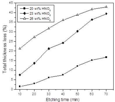
Figure 1 and 2 show the total thickness and weight loss versus the etching time, respectively for the Si etched at three different HNO3
concen-trations of 20 wt%, 23 wt% and 26 wt% mixed with 48 wt% HF. Both figures show that the
to-tal thickness and weight loss of Si wafers etched by 23 wt% and 26 wt% HNO3etchant
concentra-tions increase more rapidly as compared to the one etched by 20 wt% HNO3 etchant
concen-tration, which is the lowest among them. From the figure, the total thickness and weight loss in-crease with the increasing of etching time. The wafer thickness etched at 20 wt% HNO3
concen-tration does not show any significant variation with etching time. However, the total thick-ness loss shows a significant increase with etch-ing time at higher HNO3 concentrations of 23
wt% and 26 wt%, in which the total thickness loss for 26 wt% HNO3 is 43.06 %, which is the
highest among them, and the 20 wt% and 23 wt% HNO3 give the total thickness loss of 16.67
% and 39.40 %, respectively. The etching at 26 wt% HNO3 etchant concentration has thinned
the Si wafer into 440 µm with final weight of 0.3501 mg. Also, at 26 wt% HNO3
concentra-tion, the thickness loss variation curve becomes steeper as compare with the others, which in-dicates faster etching process occurred on the Si wafer that aggressively dissipated the sam-ple thickness. On the other hand, the variation of total weight loss shows similar behavior, in which the highest total weight loss determined for Si wafer is 9.56 % for 26 wt % HNO3,
mean-while for HNO3 concentrations of 20 wt% and
How-ever, the etching process would be active when both acids of HF and HNO3 are mixed together,
depending on the percentage of etchant concen-tration and the initial thickness of Si wafer to be etched. According to the Milind and Henry, they stated in their work that a mixture of HF and HNO3 has density and viscosity closer to
those of water [8]. Hence, the mass-transfer re-sistance or thickness of the effective transport-film for such a mixture can be quite low. Addi-tion of thick viscous acid to the mixture which does not chemically participate in the etching reaction should not alter the chemical kinetics, but should increase the mass-transfer as a result of increase in viscosity [8]. The percentage of etchant concentration would be lower than the original concentration if the initial thickness was quite thin. It is because the Si wafer would be etched faster and vigorously which lead to the bigger variation if both original percentage con-centrations was not used to mixed together.
In this study, since the initial thickness of Si wafer was only 660 µm. Thus, based on the present results, the percentage variation of total thickness and weight loss of Si wafer for 48 wt% HF/ 26 wt% HNO3 gives the best Si
thinned effect that is essential to be used in micro-electronics devices.
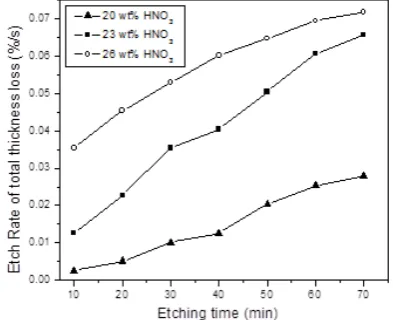
Figure 3 and 4 display the etch rate of total thickness and weight loss versus etching time, respectively for the Si etched at three different HNO3 concentrations of 20 wt%, 23 wt% and 26
wt%. The etch rate shows a decreasing trend
Figure 1. Total thickness loss versus etching time
Figure 2. Total weight Loss versus etching time
as the etching time increases, which indicates a controllable silicon thinning process can be performed in order to obtain a desired silicon wafer thickness. Furthermore, it is worth to no-tice that the etch rate of silicon wafer increases when the HNO3etchant concentration is getting
higher. This effect can be ascribed to the oxida-tion on Si surface by hole injecoxida-tion from HNO3
lead-ing to faster dioxide dissolution by HF on Si [9]. The highest etch rate of thickness loss obtained for Si wafer is 0.0718 %/s for 26 wt% HNO3
fol-lowed by 23 wt % and 20 wt % HNO3 with
max-imum etch rate of 0.0657 %/s and 0.0278 %/s, respectively. This means an appropriate etching speed can be selected dependent on the fabrica-tion condifabrica-tion. Similar effect can be observed for the etch rate determined from the total weight loss, at which the etch rate for 26 wt% HNO3
is amongst the highest for these concentrations, followed by 23 wt % and 20 wt % HNO3.
Figure 3. Etch rate of total thickness loss versus etching time
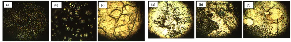
The surface image of the Si wafer before and after etching was monitored using optical micro-scope as presented in Figure 5, 6 and 7 with 100X magnification at different etching times of 10 minutes, 40 minutes and 70 minutes, re-spectively. From the figures, it can be clearly seen that there is a significant modification of Si wafer morphology, in which the Si wafer sur-face becomes smoother with clearer and brighter
Figure 4. Etch rate of total weight loss versus etching time
homogeneous structure observed as the increase of etching time and also the HNO3
concentra-tion. This observed phenomena can be due to the more diffusion limited reaction occurred on the Si wafer with better polishing efficiency at higher etching time and HNO3 concentration.
In the industry, it has been observed that addi-tion of a few viscous acids to the mixture of HF and HNO3 decreases the roughness of Si wafer
more efficiently for the same removal. Also, in-creasing the concentration of the thickener would increase the polishing efficiencies [8]. In this study, the polishing efficiency increases with in-creasing HNO3 concentration and etching time,
which leads to the formation of smooth and ho-mogeneous surface. Thus, the HNO3
concentra-tion can be increased to improve the polishing efficiency. However, at higher HNO3
Figure 5. Surface morphology of silicon wafer etched at 20% HNO3 with etching time: (a) 10
minutes, (b) 40 minutes and (c) 70 minutes.
Figure 6. Surface morphology of silicon wafer etched at 23% HNO3 with etching time: (a) 10
minutes, (b) 40 minutes and (c) 70 minutes.
Figure 8 depicts the typical XRD spectra of Si wafer etched with 23 wt% HNO3
concentra-tion at different etching times. From the figure, the intensity of etched Si wafer is higher than the pure one and increases with the increasing of etching time, which might also indicate the smoother surface formation due to removal of sil-icon dioxide after etching. From the figure, two main peaks can be observed for pure Si and also for etched Si wafer, which may correspond to the reflectance from planes of bulk and polished Si surface. Both peaks shift slightly to lower value of 2 with the increasing of HNO3 concentration,
indicating the higher values for inter planer spac-ing (d values) of atomic layers in Si. Similar effect is also observed for other HNO3
concen-trations at 20 wt% and 26 wt%, which is crucial
Figure 7. Surface morphology of silicon wafer etched at 26% HNO3 with etching time: (a) 10
minutes, (b) 40 minutes and (c) 70 minutes.
in integrated circuit fabrication.
Figure 8. XRD spectra of silicon etched at 23 % HNO3 concentration with different etching
times.
IV. SUMMARY
In summary, the etch rate of thickness and weight loss of Si immersed in the mixture of HNO3 and HF increase with the increasing of
etching time and HNO3 etchant concentration.
A smooth and homogeneous Si structure was observed when etched at higher etching time and HNO3 concentration due to polishing
increases with the increasing of etching time. Si wafer that etched with the mixtures of 26 wt% HNO3 and 48 wt% HF gives the best etching
rate when compared to the others. The present etching study indicates the etched Si can be po-tentially fitted into thinner packaged for micro-electronics products fabrication.
V. ACKNOWLEDGMENT
The authors would like to thank School of Fundamental Science and School of Ocean En-gineering, Universiti Malaysia Terengganu for the assistantships and supports for this research work.
[1] Steinert, M, Acker, J, Wetzig, K, 2008. New aspects on the reduction of nitric acid during wet chemical etching of silicon in concentrated HF/HNO3 mixtures. The Journal of Physical Chemistry, C. vol. 112, pp. 14139-14144.
[2] Kooij, ES, Butter, K, Kelly, JJ, 1999. Silicon etching in HNO3/HF solutions: Charge Balance for Oxidation Reaction. Electrochemical Solid State Letters, vol. 2, pp. 178-180.
[3] Prosenjit RC, 1997. Handbook of microlithogra-phy, micromachining and microfabrication, Vol-ume 2: micromachining and microfabrication, Society of Photo Optical.
[4] Shimura, F, 1989. Semiconductor silicon crystal technology, Academic Press, San Diego.
[5] Eyad, AR, Ibrahim, A, Hassan, A, 2017. Effect of Isopropyl Alcohol Concentration and Etching Time on Wet Chemical Anisotropic Etching of Low-Resistivity Crystalline Silicon Wafer. Inter-national Journal of Analytical Chemistry, vol. 2017, pp. 1-9.
[6] Narasimha Rao, AV, Swarnalatha, V, Pal, P, 2017. Etching characteristics of Si110 in 20 wt% KOH with addition of hydroxylamine for the fab-rication of bulk micromachined MEMS. Micro and Nano Systems Letters, vol. 5, pp. 1-9. [7] Kikuyama, H, Waki, M, Miyashita, M, Yabune,
T, Miki, N, Takano, J, Ohmi, T, 1994. A study of the dissociation state and the SiO2 etching reac-tion for HF solureac-tions of extremely low concentra-tion,Journal of the Electrochemical Society, vol. 141, pp. 366-374.
[8] Milind, SK, Henry, FE, 2000, Acid-Based Etching of Silicon Wafers: Mass-Transfer and Kinetic Ef-fects.Journal of the Electrochemical Society, vol. 147, pp.176-188.
[9] Chan, KS, Dwight, THE, 2018. Photolumines-cence, morphological and electrical properties of porous silicon formulated with different HNO3