e-ISSN: 2250-3021, p-ISSN: 2278-8719 Vol. 3, Issue 8 (August. 2013), ||V6|| PP 10-16
The Application of Dynamic Voltage Restorers (Dvr) On Power
Distribution Systems For Mitigation Of Voltage Sags / Swells
Dr.K.Ravichandrudu, V.Nalini, Mr.P.Yohan Babu, Mr.G.V.P.Anjaneyulu
1,2,3
Krishnaveni Engineering College for Women,Narasaraopet,Guntur,AP,India.
4
Reaserch scholar SVU College of engineering,S.V.U.,Tirupathi.
Abstract: - This project presents voltage sag/swell mitigation device in electric power distribution networks. Voltage sag/swell is one of the most important power quality problems challenging the utility industry. Voltage sag/swell can be compensated for voltage and power injection into distribution system. The DVR is the excellent device for dynamic responses. A new topology based on Z-source inverter is presented in order to enhance the voltage restoration property of DVR. The derived controllers are based on a suitable stabilizing damping injection scheme. The modeling of Z- source based DVR is carried out component wise and their performances are analyzed using MATLAB software. The simulation shows that the control technique is very effective and yields excellent compensation for voltage sag/swell mitigation.
I. INTRODUCTION
Modern power systems are complex networks, where hundreds of generating stations and thousands of load centers are interconnected through long power transmission and distribution networks.. However, in practice. As a result, the purity of waveform of supply lost. This ends up producing many power quality problems.. The consequence of power quality problems could range from a simple nuisance flicker in electric lamps to a loss of thousands of rupees due to power shutdown.. Power quality problems associated with an extensive number of electromagnetic phenomena in power systems with broad ranges of time frames such as long duration variations, short duration variations and other disturbances.
To compensate the sag/swell in a system, appropriate devices need to be installed at suitable locations has recently been proposed as an alternative power conversion concept as they have both voltage buck and boost capabilities. The Zsource converter employs a unique X-shaped impedance network on its dc side for achieving both voltage buck and boost capabilities this unique features that cannot be obtained in the traditional voltage-source and current-source converters. In this paper the modeling and control of voltage sag/swell compensation using Z-Source inverter based dynamic voltage restorer are simulated using MATLAB software. The simulation results are presented to show the effectiveness of the proposed control method
II. DYNAMIC VOLTAGE RESTORER
The DVR employs IGBT solid-state power-electronic switching devices in a pulse-width modulated (PWM) inverter structure and is capable of generating or absorbing independently controllable real and reactive power at its ac output terminal. Its dc input terminal is connected to an energy source or an energy storage device of appropriate capacity. The DVR is a solid-state dc to ac switching power converter that injects a set of three-phase ac output v in series and synchronism with the distribution voltages. the DVR is partial power to the load a rechargeable energy e attached to the DVR dc terminal. During normal line transmission system. For large variations (sags) in the voltages are variable thereby allowing control of the voltage conditions following the sag the energy storage reactive power exchange between the DVR and the device is recharged from the ac system by the DVR.
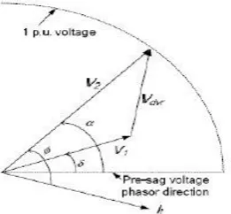
The method Widely used in present DVR control is the so called in phase voltage injection technique where the load voltage V2 is assumed to be in-phase with the pre-sag voltage.
Fig:2 Vector diagram of voltage injection
Let the voltage quantities Il, φ, δ and α represent the load current, load power factor angle, supply voltage phase angle and load voltage advance angle respectively. Although there is a phase advancement of α in the load voltage with respect to the pre-sag voltage in Fig. 2, only in-phase compensation where the injected voltage is in phase with the supply voltage (α = δ) is considered.
III. Z-SOURCE INVERTER
Z-source inverter has X-shaped impedance network on its DC side, which interfaces the source and inverter H-bridge.. The impedance network composed of split inductors and two capacitors. The supply can be DC voltage source or DC current source or AC source. Z-source inverter can be of current source type or voltage source type. Fig. 3 shows the general block diagram of Z-Source inverter.
Fig:3 Block diagram of Z-Source inverter
Source inverter operation is controlled by multiple pulse width modulation. The output of the Z-Source inverter is controlled by using pulse width modulation, generated by comparing a triangular wave signal with an adjustable DC and hence the duty cycle of the switching pulse could be varied to synthesize the required conversion. A stream of pulse width modulation is produced to control the switch as shown in fig.4. As shown in Table I, the single-phase Z-Source inverter As shown in Table I, the single-phase Z-Source inverter.
When source voltage is applied to load, two zero modes in which the inverter’s output terminals are short circuited by S1 and S3 or S2 and S4 switches and a shoot-through mode which occurs as two switches on single leg are turned on.
Applying a distinctive PWM method is necessary for ZSI considering the defined operational modes. In a symmetrical impedance network, the following equations are valid.
Fig. 5 Shoot through mode
C1 = C2 = C --- (1)
L1 = L2 = L ---- (2) I L1 = I L2 = I L (3) V C1 = V C2 = V C --- ((4)
The voltage of capacitors in a symmetric impedance network is as follows:
V i = β V dc --- (5) β = 1/[1 – 2(T0/T) --- (6)
Where, T0 and T show the shoot-through mode application period and switching period, respectively. Also, the following relation is valid in symmetric impedance networks:
Vi = 2VC –Vdc --- (7)
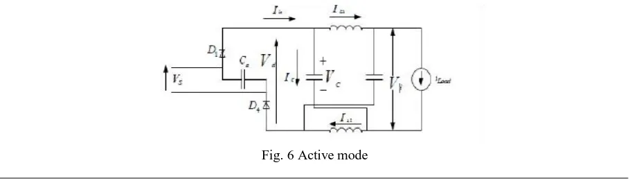
voltage. Diodes D1 and D4 are turned on if the input voltage of rectifier is positive. Diodes D3 and D2 are turned on if the input voltage of rectifier is not positive.
The equivalent circuits of rectifier fed ZSI in shoot- through and active modes are presented in Figs. 5 and 6 respectively. Fig. 7 shows the equivalent circuit of inverter in shoot-through mode. The following is obtained according to that equivalent circuit:
Vd = VL1 +VC2 --- (8) VL1 =VC1 --- (9)
Where Vd is the impedance network input voltage. Considering (4), (8) and (9), the following relation is obtained:
Vd = 2VC --- (10)
In shoot-through mode operation, the rectifier is not able to inject current and energy to impedance network. Fig. 6 shows the equivalent circuit of ZSI in active mode. Considering Fig. 6, the following relation is obtained,
Vd = Vs (t) - 2Vg --- (11)
IV. VOLTAGE SAG COMPENSATION IN DVR SYSTEM
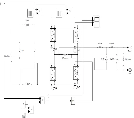
In order to meet the requirement of constant voltage control, closed loop operation is performed for the desired value of the voltage according to the need. The Simulink model of closed loop control of voltage sag compensation in a DVR system is shown in the Fig. 7. Initially the system was subjected to 25% voltage sag at t=300ms and remains up to t=700ms with the total voltage sag duration of 400ms, in a run of 1000ms.
Fig:7 Closed Loop Control of Voltage Sag Compensation in a DVR System
Fig.8 shows the subsystem 1 of the closed loop DVR system. It contains the PI controller. The AC output voltage is rectified to DC supply and then a reference voltage is given for the error. This error is sent to the PI controller. The saturator value is given as pulses for controlling the Z- Source inverter.
Fig: 8 Subsystem 1 of Closed Loop Control of Voltage Sag Compensation in a DVR System
Fig. 9 Subsystem 2 of Closed Loop Control of Voltage Sag Compensation in a DVR System.
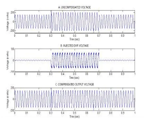
Fig.10.B shows the injected DVR voltage. Fig. 10.C gives the compensated output voltage.
In Fig. 11, the Fast Fourier Transform (FFT) analysis is performed for the compensated output voltage. Here the Total Harmonic Distortion (THD) value is 7.21%. The simulation was done under transient performance at the sag front and recovery was observed. The load voltage is maintained at the same value throughout the simulation including the voltage period. Thus voltage sag compensation using closed loop control is simulated.
Here the Total Harmonic Distortion (THD) value is 7.21%. The simulation was done under transient performance at the sag front and recovery was observed. Thus voltage sag compensation using closed loop control is simulated.
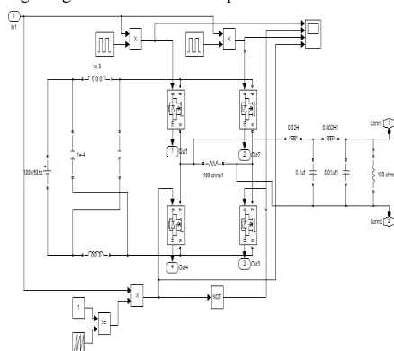
V. VOLTAGESWELL COMPENSATION IN DVR SYSTEM
Fig: 12 Closed Loop Control of Voltage Swell Compensation in a DVR System
Fig. 13 shows the subsystem 1 of the closed loop DVR system. It contains the PI controller. The AC output voltage is rectified to DC supply and then a reference voltage is given for the error.. In this case multiple pulses are given to the switch 2 and of the inverter.
Fig. 10 Simulation results of Closed Loop Control DVR under 25% sag
Fig. 13 Subsystem 1 of Closed Loop Control of Voltage Swell Compensation in a DVR System
In the Fig. 14, subsystem 2 has the Z- Source inverter which is being controlled by the PI controller. The Z-Source starts conducting when it obtains the pulse from the saturator. Fig. 15 shows the output waveform of closed loop control of voltage swell compensation. Fig. 15.A shows the uncompensated AC voltage with 30% swell. Fig.
15.B is the injected DVR voltage. Fig. 15.C shows the compensated with out voltage.
Fig. 15 Simulation results of Closed Loop Control DVR with 30% swell
Here the THD value is 6.92%. The simulation was done under transient performance at the swell front and recovery was observed. The load voltage is maintained at the same value throughout the simulation. Thus voltage swell compensation using closed loop control is simulated.
VI. CONCLUSION
In this paper voltage sag/swell compensation using Z-Source inverter based Dynamic Voltage Restorer is considered. The control technique is designed using in-phase compensation and used a closed loop control system to detect the magnitude error between voltage during pre-sag and sag periods. The modeling and simulation of closed loop contorl of voltage sag/swell mitigation were carried out using MATLAB software.
The simulation results show that the developed control technique with proposed single phase DVR is simple and efficient. From the Simulation results it was observed that dynamic voltage restorer compensates 25% of voltage sag and 30% of voltage swell.
REFERENCES
[1]. Choi S. S, Li B. H, and Vilathgamuwa D. M (2000) “Dynamic voltage restoration with minimum energy injection,” IEEE Trans. Power Systems, vol.15, pp. 51-57.
[2]. Gajanayake C. J, Vilathgamuwa D. M, and LohP. C (2005) “Smallsignal and signal-flow-graph modeling of switched Z-source impedance network,” IEEE Power Electronics Letters, vol. 3, pp. 111-116.
[3]. Jimichi T, Fujita H., and Akagi H. (2005) “Design and experimentation of a dynamic voltage restorer capable of significantly reducing an energystorage element,” in Conf. Record Industry Applications Conference,14th IAS Annual Meeting..
[4]. Loh P. C, Vilathgamuwa D. M, Lai Y. S, Chua G. T, and Li Y (2004) “Pulse-width modulation of Z-source inverters,” in Conf. Record IEEE Industry Applications Conference, 39th IAS Annual Meeting. [5]. Peng F. Z. (2003) “Z-source inverter,” IEEE Trans. Industry Applications, vol.39, pp. 504-510. [6]. Samra N. A, Neft C, Sundaram A, and Malcolm W (1995) “The distribution system dynamic voltage
restorer and its applications at industrial facilities with sensitive loads,” in Proc. Power Conversion ntell. Motion Power Quality Long Beach, CA.
[7]. Sira-Ramirez H and Ortega R (1995) “Passivity-based controllers for the stabilization of DC-to-DC power converters,” in Proc. 34th IEEE Conference on Decision and Control.