ISSN (e): 2250-3021, ISSN (p): 2278-8719
Vol. 04, Issue 06 (June. 2014), ||V3|| PP 22-31
Comparative Study of Simulated Floating Inductances Using Ota
in Low Pass Filter
Manjula V. Katageri
1, M. M. Mutsaddi
2, Rajeshwari S. Mathad
31
Government First Grade College, BAGALKOT, India
2,3
Basaveshwar Science College, BAGALKOT, India
Abstract: - Several methods of realization of floating inductance with current conveyors, current feedback
amplifier has been reported. The methods for the realization of inductance simulation with electronically tunable properties using current controlled conveyors required well matching of transistors. These devices have limited performance due to component matching. Simulation of inductance is also obtained from second generation current conveyors with excessive number of components. The simulated inductance is varied through passive elements and the approach is based on the use of current differencing buffer amplifier realized with CMOS technology and is unavailable in integrated form. Operational transconductance amplifier has an attractive feature of transconductance gain which is linearly controlled over more than 4 decades from the bias current. The OTA is a commercial low cost device and also easy to implement in monolithic integrated form. The realization of floating inductance simulation is more attractive. A commercial OTA with least number of active and passive elements exhibit an attractive method to simulate a floating inductance. A review on floating inductance using number of OTAs with resistor and single capacitor is reported in terms of searching for the best method of simulating the floating inductance in the design of low pass filter.
Key words: Floating inductance, LPF-low pass filter, OTA- Operational Transconductance Amplifier.
I.
INTRODUCTION
Floating inductance simulation is one of the important components in active filter design, oscillators and system response compensation. Several methods for realization of the floating inductance simulation have been reported [1-16]. An approach is based on second generation of current conveyors (CCCIIs), current differing buffer amplifiers (CDBAs), current feedback amplifiers (CFAs)[1,5,6,15]. The CCCII conveyors required component matching condition which is not in the view of commercial and in tunability aspect requires excessive number of active elements. Using the dual output current conveyor, the simulated inductance is varied with passive component. The approach with CDBA and CFA realization with CMOS technology is unavailable in commercial integrated form. The economic advantage in circuit design with operational transconductance amplifier (OTA) has one of the attractive features, i.e. transconductance gain which is linearly controlled over four decades. Therefore the realization technique of the floating inductance simulation based on OTA is more attractive. In this paper a review on the technique to realize the floating inductance simulation using 5-OTA, 4-OTA, 3-OTA and 2-OTA are reported and verified through software Protuse Professional 7 [ 8-13]. The validity of their values is tested in low pass filter structure explaining the agreement in values of inductance implemented in the circuit.
2. Circuit description
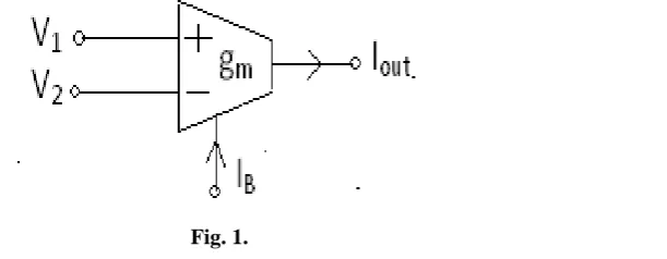
IdeallytheOTA is the voltage controlled current source, which is described mathematically as:
( (1)
Where is output current, , is transconductance gain in which VT is thermal voltage and V1 and V2
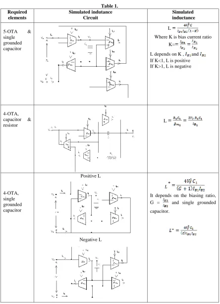
Table 1. Required
elements
Simulated indutance Circuit
Simulated inductance
5-OTA & single grounded capacitor
L
Where K is bias current ratio
K=
L depends on K , and If K<1, L is positive If K>1, L is negative
4-OTA, capacitor &
resistor L
4-OTA, single grounded capacitor
Positive L
Negative L
It depends on the biasing ratio, G = and single grounded
(Gyrator) 4-OTA & single grounded capacitor
L
for gm1=gm2=gm3=gm4=gm
3-OTA & single grounded capacitor
L
3-OTA & single grounded capacitor
L
for gm1=gm2=gm3=gm
(Gyrator) 3-OTA & single grounded capacitor
L= =
=
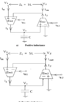
a) Positive inductance
b) Negative inductance
Fig. 2
Using the property of operational transconductance amplifier, the positive floating inductance simulation is shown in Fig. 2a, the output currents of OTA1 and OTA2 are:
( (2)
( (3)
(4)
Substitute Eqn. (4) in Eqn. (3) we get,
(5)
This gives the input impedance as:
(6)
So it is evident that the input impedance contains the inductance property as:
(7)
Thus the resulting positive inductance can be electronically varied by tuning the external bias current IB1 or IB2.
This positive inductance simulation (+L) can also occur if input terminal and output feedback is connected to negative terminal of OTA’s.
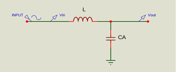
The experimental arrangement of passive low pass filter shown in Fig 3. Using all types of simulated floating inductances LPF is studied by replacing passive inductor with active inductors, which is verified by Proteus Professional 7 Software. The limitation of simulation is discussed in search of best simulation circuit for floating inductance.
CA
L
INPUT Vin Vout
Fig.3
The simulated floating inductance is verified in low pass filter with filter capacitor CA = 1nF for all bias
currents from 1µA to 2000µA of LM13600 OTA. The corresponding inductances are getting from 2.712 H to 0.678µH respectively at C1 = 1nf, which is verified in second order low pass filter, at cutoff frequency, f0 =
. The cutoff frequency response curves for all types of simulated inductance circuits are studied and are
given in Table 2.
In 5-OTA low pass filter simulation circuit it has good response for positive floating inductance at K<1. The cut off frequencies matches with theoretical values with 20% error. If K>1 for negative floating inductance the gain reduces to -200dB and fails to pass the frequency below the cut off frequency.
In 4-OTA with a resistor and single capacitor simulation circuit of low pass response the cut off frequencies does not matches with theoretical values and the low pass response is observed only above 500µA of biasing current with ripples. In another 4-OTA with only single grounded capacitor for both positive and negative inductor low pass filter, the positive floating inductor shows an exact matching of -3dB frequencies for biasing currents 1µA to 1000µA with ±6% error. The negative floating inductance low pass filter has frequency response without ripples, which does not match in cut off frequencies. This shows the 4-OTA simulator is unable to simulate negative inductance. The Gyrator 4-OTA low pass filter shows a good response for positive inductance for all bias currents of 1µA to 2000µA with an error of ±6%. In negative simulation inductance low pass responses have without ripples and shows its cut off frequencies matches with -6dB frequencies.
In 3-OTA simulated inductance circuits, the first two circuits shows the simulation occurred with ±30% and ±7% error respectively, which are observed through low pass filter. The ripple of the first circuit is less compared to second circuit. The third, gyrator 3-OTA circuit shows for all biasing currents form 1µA to 2000µA the cut off frequencies matches with -6dB frequencies instead of -3dB without ripples, which is similar with responses of negative inductance simulator of 4-OTA Gyrator low pass circuit.
The proposed 2-OTA floating simulated inductance circuit of low pass response shows the simulation is carried with ±5% error with ripples at cutoff frequencies in positive inductance. The 2-OTA negative floating inductance also shows the same responses as 4-OTA and 3-OTA negative gyrator circuit, i.e. cut off frequencies that are matching with -6dB frequencies. This shows the Bessel’s filter parameter structure.
Table 2.
5-OTA+C 3 4 5 11 6 1 2 7 8 U1:A LM13600 14 13 12 11 6 16 15 10 9 U1:B LM13600 3 4 5 11 6 1 2
7 8 U2:A
LM13600 14 13 12 11 6 16 15 10 9 U2:B LM13600 3 4 5 11 6 1 2 7 8 U3:A LM13600 C1 1nF CA 1nF U1:B(V-) U1:B(V+) U1:A(AMPBIAS) VALUE=600u input out1 U3:A(AMPBIAS) VALUE=200u
For K<1( f0=420KHz )
IB1=IB2=IB3=200µA and IB4=IB5=100µA
For K>1 at IB1=IB2=IB3=100µA and
IB4=IB5=200µA
4-OTA+C+R 3 4 5 1 1 6 1 2 7 8 U1:A LM13600 14 13 12 1 1 6 1 6 1 5 1
0 9 U1:B
LM13600 3 4 5 1 1 6 1 2 7 8 U2:A LM13600 14 13 12 1 1 6 1 6 1 5 1 0 9 U2:B LM13600 R1 10k C1 1nf U1:B(V-) U1:A(V+) input out1 CA 1nf U2:B(AMPBIAS) VALUE=1000u U1:B(AMPBIAS) VALUE=1000u
L=1.041mH,C=1nf, (f0)th=155.8KHz
(f0)pr = 623.0KHz
4-OTA+C(positive L) 3 4 5 11 6 1 2 7 8 U3:A LM13600 14 13 12 11 6 16 15 10 9 U3:B LM13600 14 13 12 11 6 16 15
10 9 U4:B
LM13600 3 4 5 11 6 1 2 7 8 U4A LM13600 C11 1nf CAA 1nF U4A(AMPBIAS) VALUE=400u U3:A(V-) U3:A(V+) input2 ou t2
L = 134µH, C=1nf, (f0)th=434.3KHz
(f0)pr = 422.0KHz
4- OTA (Negative L) L = 268µH, C=1nf, (f0)th=307.1KHz
3 4 5 11 6 1 2 7 8 U1:A LM13600 14 13 12 11 6 16 15 10 9 U1:B LM13600 3 4 5 11 6 1 2 7 8 U2:A
LM13600 14 13 12 11 6 16 15 10 9 U2:B LM13600 C1 1nf CA 1nF U2:B(AMPBIAS) VALUE=400u U1:A(V-) U1:A(V+) input1 ou t1 4-OTA Gyrator For positive feedback L
3 4 5 1 1 6 1 2 7 8 U:A LM13600 14 13 12 1 1 6 1 6 1 5 1 0 9 U:B LM13600 3 4 5 1 1 6 1 2 7 8 U:AA LM13600 14 13 12 1 1 6 1 6 1 5 1 0 9 U:BB LM13600 C1 1nf
input 1 output1
U:A(V+) U:B(V-) CA 1nf U:AA(AMPBIAS) VALUE=400u
For negative feedback L
3 4 5 1 1 6 1 2 7 8 U1:A LM13600 14 13 12 1 1 6 1 6 1 5 1 0 9 U1:B LM13600 3 4 5 1 1 6 1 2 7 8 U2:A LM13600 14 13 12 1 1 6 1
6 15
1
0 9 U2:B
LM13600 C1 1nf input output U1:A(V+) U1:B(V-) CA 1nf U2:A(AMPBIAS) VALUE=2000u
L = 271.0µH, C = 1nf, (f0)th=305.0KHz
(f0)pr = 315KHz
L = 271.0µH, C = 1nf, (f0)th=305.0KHz
(f0)pr = 196KHz(-3dB), 304KHz(-6dB)
3-OTA +C L = 1.084mH, C = 1nf, (f0)th=152.8KHz
3 4 5 1 1 6 1 2 7 8 U1:A LM13600 14 13 12 1 1 6 1
6 15
1
0 9 U1:B
LM13600 3 4 5 1 1 6 1 2 7 8 U2:A LM13600 C1 1nf CA 1nf U1:B(V-) U1:A(AMPBIAS) VALUE=150u input o u t1 U1:B(V+) 3-OTA +C 3 4 5 1 1 6 1 2 7 8 U1:A LM13600 14 13 12 1 1 6 1 6 1 5 1 0 9 U1:B LM13600 C1 1nF CA 1nF 3 4 5 1 1 6 1 2 7 8 U2:A LM13600 U1:A(AMPBIAS) VALUE=150u U1:B(V+) U1:A(V-) input out1
L = 1.084mH, C = 1nf, (f0)th=152.8KHz
(f0)pr = 159.0KHz
3-OTA +C (Gyrator)
3 4 5 11 6 1 2 7 8 U1:A
LM13600 14 13
1 2 11 6 16 15 10 9 U1:B LM13600 3 4 5 11 6 1 2 7 8 U2:A LM13600 C1 1nF U1:A(AMPBIAS) VALUE=150u U2:A(V-) U2:A(V+) input out1 CA 1nf
L = 1.084mH, C = 1nf, (f0)th=152.8KHz
(f0)pr = 98.0KHz(-3dB), 153KHz(-6dB)
2-OTA+C For positive L
L = 271.0µH, C = 1nf, (f0)th=305KHz
3 4
5
11 6
1 2
7 8
U1:A
LM13600
1
4
1
3
1
2
11 6
16 15 10
9
U1:B
LM13600 U1:A(V+)
U1:B(V-) U1:B(AMPBIAS)
VALUE=200u
CA
1nf
C1
1nf
input output
For negative L
3 4
5
11 6
1 2
7 8
V1:A
LM13600
1
4
1
3
1
2
11 6
16 15 10
9
V1:B
LM13600 V1:A(V+)
V1:B(V-) V1:B(AMPBIAS)
VALUE=80u
C1I
1nf input
CAA
1nf output
L = 271.0µH, C = 1nf, (f0)th=305KHz
(f0)pr = 196KHz(-3dB), 305(-6dB)
II.
CONCLUSION
The simulation of floating inductance with less number of commercially available active devices with single grounded capacitor is one of important aspect of design in filter application. The tunable property of transconductance gain of OTA, the simulation of floating inductance with 2-OTA gives exactly matching frequencies with less error compared with 5-OTA, 4-OTA and 3-OTA low pass responses. The negative inductance simulation cut off frequencies matches with -6dB frequencies, which shows Bessel’s filter characters. It is concluded that 2-OTA floating inductance simulation of positive and negative inductance is considered to be more suitable in LC ladder filter structures.
III.
ACKNOWLEDGEMENT
Authors of the paper acknowledge the help rendered by VGST for studying the filter properties and simulation techniques under the project “Active filter design and their applications in high frequency region”. We acknowledge the Principal and staff of Bharata Ratna C.N.R. Rao, research centre of BVVS Basaveshwar Science College Bagalkot
REFERENCES
[1] A.U. Keskin and E. Hangeioglu, CDBA based synthetic floating inductance circuits with electronic tuning properties, ETR J, Vol 27, No-2, 2005, 239-242
[2] Abdullah Ferikoglu, Toner Topal, Inductor Simulation With Operational Devices”, G.U. Journal of
Sciences , Vol. 18(1),2005,143-151
[3] Khanittha Kaewdang, K. Kumwachara and W.Surakampontorn, Electronically Tunable Floating CMOS Resistor Using OTA,IEEE ISCIT,2005, 705-708
[4] Shahram Minaei, Erkan Yuce, Oguzhan Cicekoblu, Lossless active floating inductance simulator, Third
IEEE International workshop on electronic design, tests and applications, 2005
[5] H. Kuntman, M Gulsoy,O. Cicekoglu, Actively Simulated Grounded Lossy Inductors Using Third Generation Current Conveyors, Elsevier, Microelectronics Journal 31, 2000 , 245-250.
[7] W. Kiranon and P. Pawarangkoon, Floating Inductance Simulation Based On Current Conveyors,
Electronics letters, Vol. 33, No. 21, 1997, 1748- 1749
[8] Ivan S. Uzunov : Theoretical Model Of Ungrounded Inductance Realized With Two Gyrators, IEEE
Transactions on circuits and systems ,Vol-55,No.10 [2008], 981-985
[9] Wandee Patechmaneelumka : Simple Floating Inductance Simulators Using OTAs, IEEE, International
instrumentation and measurement Technology Conference, Singapore, May 2009, 5-7
[10] Wandee Patechmaneelumka : OTAs-based Positive/Negative floating inductance simulator, International
Multi Conference of Engineers and computer Scientists ,Vol. II, Hong Kong, [ March 2009]
[11] Priyanka Soni, Pr.B.P.Singh, Monika Bhardwaj: Design of OTA based Floating inductor, IEEE,2011 [12] Kittisik Longsomboon, Wandee Petchmaneelumka, Thepjit Cheypoca and Vanchai Riewruja : OTA-
based Electronically variable Floating inductance simulator, International Conference on Control,
Automation and systems Korea, 2011,221-224
[13] Neha Gupta, Meenakhi Sutar, Sapna Singh, Priyanka Soni : Active Filter Design Using Two OTA Based Floating Inductance Simulator, International Journal of VLSI & Single Processing Applications, Vol2,[Feb 2012], 47-50
[14] Abhishek Saini, Ankit Aswal, Ajit Singh, Flooded Cascade OTA Based Gm-C Filter Designing , Int.J. Of
Advanced Research In Electronics And Communications Engineering (IJARECE) Vol.2, Issue 9, 2013
[15] Bhaskar, R.Senani, Raj, Simulation Of A Floating Inductance: A New Two CFOA Based Configuration”