EFFICIENT AND EFFECTIVE ECO-FRIENDLY
VEHICLES
Kanchanamala
1, V.Priya
21
Student, Power Electronics and Drives, CSI College of Engineering, Tamil Nadu, (India)
2
Assistant Professor, Electrical and Electronics, CSI College of Engineering, Tamil Nadu, (India)
ABSTRACT
This paper proposes a high gain non –isolated soft switching bi- directionaldc–dc converter. This converter is
suitable for high step-up and step-down applications. The proposed converter can achieve zero voltage
switching turn on of all switches and zero-current-switching turn off of some switches in continuous conduction
mode in both forward and reverse modes. This improves efficientcharge of regenerative energy as well as
voltage boost and regulation for efficient operation of inverters and motors. An optimized switching strategy is
presented to minimize switch current rating and achieve soft switching in wider range. An intermediate
switching pattern is introduced to carry out seamless mode change. Experimental results from a 5-kW prototype
are provided to validate the proposed concept.
Keywords: Bi-Directional Dc–Dc Converter (BDC), Continuous Conduction Mode (CCM), High
Step-Up, High Voltage Gain, Non-Isolated, Soft Switched.
I. INTRODUCTION
1.1 Existing System
The basic nature and the previous work has been with the bi-directional converter using switched capacitor cells.
The BDC using switched-capacitor converter cells could have more modular structure and higher power
handling capability, but the required number of switches becomes high . They are hard-switched, and high
current pulse occurs since two capacitors with different voltages are connected in parallel at each switching
instant. A major drawback of the switched capacitor- based converter is that ESR(electric series resistance) drop
of the active and passive devices is considerable due to high number of series connected devices in the current
path, resulting in reduced output voltage.
1.2 Proposed System
In this paper, a new non isolated BDC for high step-up/step down and high-power applications is proposed. The
optimized PWM switching technique for boost and buck operations and smooth mode transition is also
presented. The proposed converter has the following advantages:
1) High voltage gains for both boost and buck operations;
2) Reduced (nearly half) voltage stresses of switches;
3) ZVS turn on and ZCS turn off of switches in CCM operation;
4) reduced energy volumes of passive components;
1.3 Hybrid Vehicle
Hybrid passenger cars have been on the market since 1997, with hybrid buses and delivery trucks emerging in
the last 3-4 years. Widespread use in industrialized markets is now leading to use in developing countries
through second hand markets. A well-functioning and efficient transport sector is a requirement for economic
and social development, bringing people together and enabling the trade and exchange of goods and ideas.
However, the transport sector is also responsible for a number of negative social and environmental effects,
including a significant contribution to global greenhouse gas emissions and air pollution.
II. MODELING OF EFFICIENT AND EFFECTIVE ECO-FRIENDLY VEHICLE
The principle parts and functions of efficient and effective eco-friendly vehicles are explained in this session. A
bock diagram is a specialized, high-level type of flowchart. Its highly structured form presents a quick overview
of major process steps and key process participants, as well as the relationships and interfaces involved. A block
diagram is a useful tool both in designing new processes and in improving existing processes. In both cases the
block diagram provides a quick, high-level view of the work and may rapidly lead to process points of interest.
2.1 Block Diagram
Fig.1.Block Diagram of Efficient and Effective Eco Friendly System
2.2 Components of Block Diagram
2.2.1 Rectifier Circuit
A rectifying circuit is one which links an AC supply to dc load, that is, it converts an alternating voltage supply
to a direct voltage. Here the rectifier used is a full bridge rectifier.A rectifier utilizes unidirectional conducting
device ex: P-N junction diode.
2.2.2 Bi-Directional Converter
A bi-directional converter is a device which converts alternating-current power to direct-current power and
vice-versa. The converter is based on a cascaded buck-boost structure with active snubber circuits in order to achieve
zero voltage and zero current transition, showing high efficiency.
2.2.3 Pulse Generator
A pulse generator is either an electronic circuit or a piece of electronic test equipment used to generate
rectangular pulses.Simple bench pulse generators usually allow control of the pulse repetition rate (frequency),
pulse width, delay with respect to an internal or external trigger and the high- and low-voltage levels of the
pulses. More-sophisticated pulse generators may allow control over the rise time and fall time of the pulses.
Pulse generators are available for generating output pulses having widths (duration) ranging from minutes down
2.2.4 Inverter
A power inverter, or inverter, is an electronic device or circuitry that changes direct current (DC) to alternating
current (AC).The input voltage, output voltage and frequency, and overall power handling depend on the design
of the specific device or circuitry. The inverter does not produce any power; the power is provided by the DC
source. A power inverter can be entirely electronic or may be a combination of mechanical effects (such as a
rotary apparatus) and electronic circuitry. Static inverters do not use moving parts in the conversion process.
2.2.5working
Initially an AC supply is given. Then the rectifier circuit converts the AC to DC supply and the output is filtered
and given to the bi-directional converter and the final results is viewed in the cathode ray oscilloscope.
III. BI-DIRECTIONAL DC-DC CONVERTER
This paper presents a power converter for a fuel cell electric vehicle driving system. A new bidirectional,
isolated topology is proposed in consideration of the differing fuel cell characteristics from traditional
chemical-power battery and safety requirements. The studied converter has the advantages of high efficiency, simple
circuit, and low cost. The detailed design and operating principles are analysed and described. The simulation
and experimental waveforms for the proposed converter are shown to verify its feasibility. The proposed
converter achieves zero-voltage switching (ZVS) for the entire main switches and zero-current switching for the
rectifier diodes in the large-load range. These features reduce switching loss, voltage and current stresses, and
diode reverse-recovery effect. A typical non-isolated bi-directional dc-dc converter technology is to combine a
buck converter and a boost converter in a half-bridge configuration.In this paper, a new non-isolated BDC for
high step-up/step-down and high-power applications is proposed. The optimized PWM switching technique for
boost and buck operations and smooth mode transition is also presented.
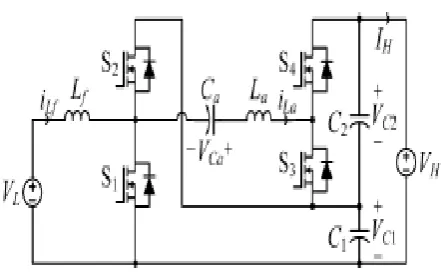
Figure 2.shows the circuit diagram of the proposed BDC. The proposed converter consists of a general
half-bridge converter as the main circuit and an auxiliary circuit that includes the capacitor Ca, inductor La, and two
high-voltage side (HVS) switches S3 andS4 . The goal of control, in this paper, is assumed to regulate the HVS
voltage VH, while allowing bidirectional power flow according to the direction of inductor current
ILf.Operating Principle is assumed that capacitances C1, C2, and Ca are large enough so that voltages VC1,
VC2, and VC across them are constant during the switching period TS.
3.1 Boost Operation (Forward Mode)
Figs.3. and fig.4 show key waveforms and operation states of the boost operation, respectively. In this mode,
low-voltage side (LVS) switches S1and S2are operated with asymmetrical complementary switching with duty
cycles of D and 1−D, respectively. In the meantime, HVS switches S3 and S4 are turned ON with delay times of
td3and td4, respectively. The operation of the proposed converter can be divided into five modes.
Fig.3. Key Waveforms of the Proposed Converter (Boost Operation)
Fig.4 Operation States pf Proposed Converter (Boost Operation)
Mode I operation: This mode I [t0 –t1], begins with turning OFF of S2and S4. Then, the body diodes of S1 and
S4 are turned ON. The gating signal for S1 is applied with appropriate dead-time during this mode, and then S1
could be turned ON under ZVS condition. Inductor currents iLfand iLastart to increase and decrease,
respectively, with the slopes determined by the following equations:
diLf/dt= VL/Lf…...……(1)
Mode II operation: In this mode II [t1–t2], the increasing current iLfbecomes greater than the decreasing current
iLa, current flowing through S1 is reversed, and the main channel of S1 conducts. This mode ends when the
decreasing current iLareaches 0 A. Note that switchS4 is also turned OFF under ZCS condition.
Mode III operation: In this mode III [t2 –t3], at t2 current iLais reversed and the body diode of S3 is turned ON.
For synchronous rectification the gating signal for S3 can be applied after t2. Note that S3 is turned ON under
ZVS condition. Inductor current iLalinearly increases with the slope determined by the following equation:
diLa/dt=[VCa− VC1]/La……... (3)
Both inductor currents iLfand iLaflow through switch S1.
Mode IV operation: In this mode IV [t3–t4],att3switches S1 and S3 are turned OFF, and then body diodes of S2
and S3 are turned ON. Both inductor currents iLfand iLastart to decrease with the slopes determined by the
following equations:
diLf/dt= [VL − VC1]/Lf………(4)
diLa/dt= VCa/La……... (5)
The gating signal for S2 is applied with appropriate dead-time during this mode, and then S2 could be turned
ON under ZVS condition. This mode ends when the decreasing current iLareaches 0 A. Note that switch S3 is
also turned OFF under ZCS condition.
Mode V operation: This mode v [t4 –t5], begins when current iLa is reversed and the body diode of S4 is turned
ON. For synchronous rectification, the gating signal for S4 can be applied after t4 .Note that S4 is turned ON
under ZVS condition. Inductor current iLa linearly increases with the slope determined by the following
equation:
diLa/dt = [VCa − VC2]/La……… (6)
This is the end of one complete cycle.
3.2 Buck Operation (Reverse Mode)
Fig.5 show key waveforms and Fig.6.shows operation states of the buck operation, respectively. In this mode,
HVS switches S3 and S4 are operated with asymmetrical complementary switching with duty cycles of D and
1−D, respectively. In the mean time, LVS switch S2 is turned ON with delay time of td2. The operation of the
proposed converter can be divided into six modes.
Fig.6.Operation States of Proposed Converter (Buck Operation)
Mode I operation: This mode I [t0-t1] begins with turning OFF of switches S2 and S4. Then, the body diodes of
S1 and S3 are turned ON after the parasitic capacitors of S3 and S4 are completely discharged. Inductor current
iLf starts to decrease.
Mode II operation:This mode II [t1–t2] at t1 inductor current iLa starts to decrease with the slope. After
appropriate dead-time switches S1 and S3 are turned ON. The gate signal for S3 should be applied before
reversal of current iLa for ZVS turn ON. Note S1 is turned ON without any delay for synchronous rectification.
This mode ends when the decreasing current iLa reaches 0 A.
Mode III operation: This mode III [t2–t3] at t2 inductor current iLa is reversed and starts increasing with
slope.the positive peak value of iLa can be obtained as follows:
ILa+ = [VCa − VC1]/La*[DTS − VC2] · 2 · COSS/La]…..(7)
Where, COSS is the output capacitance of the switch.
Mode IV operation :This mode IV [t3–t4], Switches S1 and S3 are turned OFF at t3, and the n body diodes of
S1 and S4 are turned ON. Inductor current iLa starts to decrease with the slope determined by (2). Note that S4
could be turned ON under ZVS condition if the gate signal for S4 is applied with appropriate dead-time before
reversal of current iLa. This mode ends when the decreasing current iLa reaches 0A.
Mode V operation:In mode V [t4–t5], the increasing current iLa becomes greater than the decreasing current
iLf, body diode of S1 is turned OFF under ZCS condition. Then, after parasitic capacitors of S1 and S2 are
completely charged and discharged, respectively, the body diode of S2 is turned ON and inductor currents iLa
and iLf start to decrease and increase, respectively, with slopes. The negative peak value of iLa is determined by
the following equation:
ILa− = ILf +ΔILf/2− VC1/ ………(8)
Where, ΔILf is current ripple of Lf. For ZVS turn on of S2, the gate signal for S2 should be applied before the
decreasing current iLa becomes smaller than the increasing current iLf.
Mode VI operation: This mode VI [t5–t6], at t5 switch current iS2 is reversed. Inductor currents iLa and iLf
keep decreasing and increasing with slopes. At the end of this mode S2 and S4 are turned OFF. This is the end
of one complete cycle.
The explained above are the two different modes of operation, the forward mode (boost operation) and reverse
IV. SIMULATION AND ANALYSIS OF EFFICIENT AND EFFECTIVE ECO-FRIENDLY
VEHICLES
Simulation and analysis of high gain soft switching bi-directional dc-dc converter for eco-friendly vehicles is
demonstrated using MATLAB Simulink software. Each and every component is designed using
MATLAB/SIMULINK and Sim Power System software package to verify the effectiveness of the system.
4.1 Matlab Simulation of Forward Direction
The interleaving technique can be applied to reduce the size of passive components and current stresses. A
5-kW prototype of the two-phase interleaved version of the proposed converter shown in Fig. 5.1 was built
according to the following specification: Po = 5 kW, fs = 30 kHz, VH = 400 V, VL = 72–100 V, Lf = 130 μH, La
= 13 μH, Ca = 30 μF, C1=C2 =470 μF.
Fig.7.Simulation Circuit for Forward Direction
4.2 Waveforms of Forward Direction
Below shows the input and output voltage waveform of forward direction.
4.3 Matlab Simulation of Reverse Conduction
Fig.9. Simulation Circuit for Reverse Direction
4.4 Waveforms of Reverse Conduction
Fig.10.Output Waveform of Input Voltage and Output Voltage
4.5 Modified Matlab Simulation of Forward Direction
The Simulink model used for the implementation of modified high gain soft-switching bidirectional dc–dc
converter for eco-friendly vehicles.
4.6 Inputwaveforms of Forward Direction
Fig.12 Waveform of Input Voltage and Output Voltage
4.7 Modified Matlab Simulation of Reverse Direction
Fig.13 Modified Simulation Circuit for Reverse Direction
4.8 Inputwaveforms of Reverse Direction
It is seen that there are no transients caused by change of switching patterns during the mode change. The
measured efficiencies under different LVS voltage conditions in forward and reverse modes.
4.9 Comparison
The comparison of the proposed converter circuit and modified converter circuit is analysed and found out that,
in the modified converter circuit the regenerative capability is being improved and net efficiency of the
eco-friendly vehicle is improved to a higher level.
V. CONCLUSION
In this paper, a non-isolated soft switching BDC has been proposed for high voltage gain and high-power
applications. The proposed converter can achieve ZVS turn on of all switches and ZCS turn off some switches
in both boost and buck operations. An optimized switching sequence has been presented along with an
intermediate switching pattern to carry out seamless mode change. A 5-kW prototype of the proposed converter
has been built and tested to verify the validity of the proposed operation. A nominal duty cycle of 0.64 was used
to achieve voltage gain of 5.5. The maximum efficiencies in forward and reverse modes are 97.9% and 97.7%,
respectively. It has also been shown in the experiment that the mode change is seamless due to the proposed
switching sequence. In future, grid connected applications like a solar roof panel for the hybrid vehicle, which
makes it’s a renewable application improved battery backup and regenerative capability and hence overall
improvement of efficiency is being worked on.
VI. ACKNOWLEDGEMENT
First and Foremost, I owe my colossal gratitude to the ALMIGHTYGOD for blessing me with his grace and
taking my endeavour to a successful culmination. I am highly obliged to express my sense of gratitude to
the Principal of our institution Dr.GeorgeChellianChandran,B.E., M.E., Ph.D., PGDBM., Head of the
Department Prof.P. Pradeepa, B.E., M.E.,(Ph.D)., andto my guide Miss.V. Priya, B.E.,M.E.,Asst. Professor,
Electrical and Electronics Engineering.
REFERENCES
[1] Minho Kwon,”High Gain Soft-Switching Bidirectional DC–DCConverter for Eco-Friendly Vehicles”,
IEEE Transactions on Power Electronics, vol. 29, no. 4, april 2014.
[2] J. Zhang, R. Y. Kim, and J. S. Lai, “High-Power density design of a soft- switching high-power
bidirectional DC-DC converter,” in ProcIEEEPower Electron. Spec. Conf., 2006, vol. 2, pp. 1–7.
[3] Y. Du, X. Zhou, S. Bai, S. Lukic, and A. Huang, “Review of non-isolated bi-directionalDC–DC converters
for plug-in hybrid electric vehicle charge station application at municipal parking decks,” in Proc. 25th
IEEE Appl. Power Electron. Conf. Expo., 2010, pp. 1145–1151.
[4] W. Li, X. Lv, Y. Deng, J. Liu, and X. He, “A review of non-isolated high step-up DC/DC converters in
renewable energy applications,” in Proc. 24th Annu.IEEE Appl. Power Electron. Conf. Expo., Washington,
DC, USA, Feb. 15–19, 2009, pp. 364–369.
[5] Muhammad H. Rashid, Power Electronics Circuits Devices and Applications (Pearson, Noida 2012).