Available Online at www.ijpret.com 464
INTERNATIONAL JOURNAL OF PURE AND
APPLIED RESEARCH IN ENGINEERING
AND TECHNOLOGY
A PATH FOR HORIZING YOUR INNOVATIVE WORK
DESIGN OF HIGH SPEED ALU USING REVERSIBLE LOGIC GATES BASED ON
VEDIC MATHEMATICS
SHRUTI D. KALE, GAURI N. ZADE
DATTA MEGHE COLLEGE OF ENGINEERING TECHNOLOGY & RESEARCH CENTRE WARDHA
Accepted Date: 15/03/2016; Published Date: 01/05/2016
\
Abstract- In modern times reversible logic fascinate notable attention to produce something
better in certain fields like nanotechnology, quantum computing and low power design. This work is devoted for the design of an Arithmetic module with high speed and low power dissipation. In this project addition and multiplication are considered as main functions, because these functions affect the speed of operation and causes power dissipation. Reversible logic has shown potential to have extensive applications in emerging technologies such as quantum computing, optical computing, DNA computing to produce almost zero power dissipation under ideal conditions. The speed of ALU has been improved using ancient system of mathematics which is Vedic mathematics. It has a unique technique of calculations based on 16 Sutras and 13 Upa-sutra. The designing using reversible logic reduce power dissipation in terms of TRLIC. In this project both technic utilized and designed circuit achieved high speed and less power dissipation as resultant TRLIC is optimized.
Corresponding Author: SUKANTI B. MARDOLKAR Access Online On:
www.ijpret.com
How to Cite This Article:
Shruti D. Kale, IJPRET, 2016; Volume 4 (9): 464-472
Available Online at www.ijpret.com 465 due to its ability to reduce the power dissipation which is the main requirement in low power digital design.
Conventional logic circuits dissipate a significant amount of energy because bits of information are erased during the logic operations. Thus, if logic gates are designed such that the information bits are not destroyed, the power consumption can be decrease dramatically. The information bits are not lost in case of a reversible computation.
System Model Description
Reversible Logic gates:-
In the recent past, Reversible logic has more demand due to its less heat dissipating characteristics. Many researches have been performed with the efforts on design and synthesis of efficient reversible logic circuits. Reversibility shows that no information about the computational states can lose, so we can recover any previous stage by computing backwards or uncomputing the results. This is termed as logical reversibility. It has been proved that, any Boolean function can be executed logically using reversible gates. The design of reversible logic circuits consider following points to achieve an optimized circuit.
They are:-
i) Fan-out is not allowed.
ii) Loops or feedbacks are not allowed. iii) Garbage outputs must be less in numbers. iv) Reduced delay.
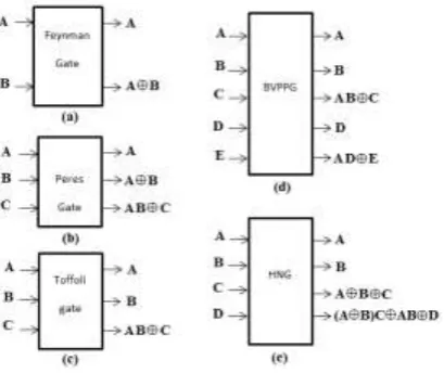
Available Online at www.ijpret.com 466 Figure 1: Reversible Logic Gates
Optimized Parameters for Reversible Logic Circuits:-
Constant Inputs (CI):- Number of inputs that are to be sustained constant at either ‘0’ or ‘1’.
Garbage Outputs (GO):- Number of outputs that are not used in the synthesis of a given function. These are vital part of the reversible designing.
Gate Count (GC):- Number of gates required for the design of function.
Quantum Cost (QC):- It is the cost of the circuit in terms of the cost of a basic gate. Quantum cost calculation depends on the number of gates required to realize the circuit.
Total Reversible Logic Implementation Cost (TRLIC):- TRLIC is the summation of Constant Inputs (CI), Garbage Outputs (GO), Gate Count (GC) and Quantum Cost (QC). It is given by- TRLIC= ∑ (CI + GO + GC + QC)
Urdhva Tiryagbhyam:-
The formula simply means: “Vertically and crosswise”
Urdhva Tiryagbhyam sutra is a general multiplication formula applicable to all cases of multiplication. The digits on the both sides of the line are multiplied and added with the carry from the previous step. This generates one of the bits of the result and a carry. This carry is added in the next step and hence the process goes on. If more than one line are there in one step, all the results are added to the previous carry. In each step, least significant bit acts as the result bit and all other bits act as carry for the next step. Initially the carry is taken to be zero.
2x2 Bit UTMModule:
Available Online at www.ijpret.com 467 Figure 2: The Vedic Multiplication Method for Two 2-Bit Binary Numbers
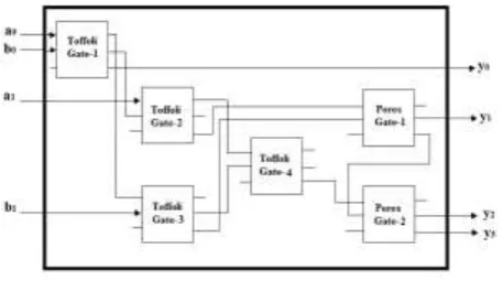
The reversible logic design for 2-bit vedic multiplication is possible by the use of four Toffoli gates and Two Peres gates [9] is as shown in figure (3).
Figure 3: 2x2 Bit UTM Module.
The circuit shown in figure (3) has total quantum cost of 28, number of garbage outputs 6 with constant inputs 6 and gate count is 6. Including everything the performance of UTM is scaled up and optimized.
But further optimization is possible with the use of BVPPG gate, three Peres gates and one Feynman gate. The Modified 2X2 Vedic multiplier module is implemented usinga reversible logic gate which is shown in Figure (4). This design has total quantum cost of 23, number of gates required to design multiplier is 5 along with total garbage outputs are 5 and constant inputs are 5.
5-Bit Ripple Carry Adder Module:
Available Online at www.ijpret.com 468 Figure 4: Modified 2x2 Bit UTM.
Figure 5: 5-Bit Ripple Carry Adder
5-Bit ripple carry adder design has total quantum cost of 28, number of gates are 5, with total garbage outputs are 9 and constant inputs are 5.
4-Bit Ripple Carry Adder Module:
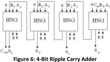
The 4-bit adder circuit form with four HNG gate is as shown in Figure (6). Here HNG gate which acts as full adder, the resultant output S0 (sum) and carry forward to next HNG gate, like wise S1, S2 and S3 generated.
Figure 6: 4-Bit Ripple Carry Adder
Available Online at www.ijpret.com 469 Figure 7: 2-Bit Ripple Carry Adder
2-Bit ripple carry adder design has total quantum cost of 8, number of gates are 2, with total garbage outputs are 2 and single constant input.
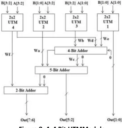
Vedic Multiplier for 4x4 Bit UTM Module:
The circuit of 4x4 bitUTM consist four 2x2 UTM, one 5-bit carry ripple adder, one 4-bit carry ripple adder and one 2-bit carry ripple adder as shown in Figure (8). The resulted Vedic multiplier can be used to reduce delay. Interestingly, 8x8 Vedic multiplier modules are implemented easily by using four 4x4 multiplier modules.
Available Online at www.ijpret.com 470 Observation
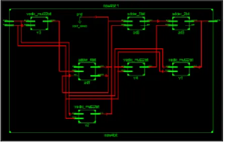
Figure 9: RTL Schematic of 4x4 Bit UTM Module
The RTL Schematic view of internal architecture of 4x4 UTM is as shown in Figure (9).
Figure 10: Simulation Result of 4x4 Bit UTM Module.
To verify the result, assume two 4-bit numbers as, a=10 (1010) and b=10 (1010) the resultant output is of 8-bit Out=100 (01100100). The simulation results for this case are shown in Figure (10) and corresponding design summary table is given in Table 1.
Table 1: Design Summary of 4x4 Bit UTM
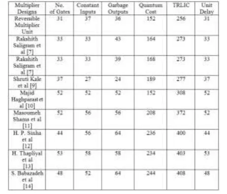
RESULT & COMPARISON
The Reversible Multiplier Unit attains a significant improvement in performance with Vedic calculations and reversible way of design. The important constraints for any reversible logic design consist of-
i) Reversible logic circuits should have minimum quantum cost.
Available Online at www.ijpret.com 471 Conclusion and Future scope
Along with reversible logic Vedic mathematics is a gift given to this world by the ancient sages of India. Reversible logic gates reduce power dissipation thus reversible ALU consume less power and Vedic mathematics which is well known for high speed operation, resulting ALU achives high speed. By utilizing beneficial features of low power and high speed has been implemented for design of ALU. On comparing withprevious multiplier design, the project design found more optimized.
An important aspect of designing circuits using reversible logic gates is to reduce the power dissipation which directly affects TRLIC. Future work could be extended to optimizing TRLIC by minimizing the garbage outputs and constant inputs in the circuit.
REFERENCES
1. R. Landauer,“Irreversibility and Heat Generation in the Computational Process,”IBM Journal of Research and Development, vol. 5, pp. 183-191, 1961.
2. C.H. Bennett, “Logical Reversibility of Computation,”IBM Journal of Research and Development, 17:525-532, November 1973.
3. E. Fredkin and T, Toffli, “Conservative Logic,” Int. J. Theor. Phys, vol. 21, pp. 219-253, 1982.
4. R. Feynman, “Quantum mechanical computers,”Opt. News, vol. 11, pp. 11-20, 1985. 5. Anvesh Kumar, National institute of technology, Jalandhar, India, Ashish Raman “Low Power ALU Design by Ancient Mathematics”, Computer and Automation Engineering IEEE, PP: 862-865, 2010.
Available Online at www.ijpret.com 472 7. Rakshith Saligram, Rakshith T. R., “Optimized Reversible Vedic Multipliers for High Speed Low Power Operations,” IEEE Conference on Information and Communication Technologies, 2013
8. Miss. Shruti D. Kale, “Study of Reversible Logic Circuits”, International Journal of Application or Innovation in Engineering & Management (IJAIEM), Volume 4, Issue 12, December 2015.
9. Miss. Shruti D. Kale and Prof. Gauri N. Zade, “Design Vedic Multiplier Using Reversible Gates”, International Journal of Scientific & Engineering Research (IJSER), Volume 7, Issue 1, January-2016.
10. Majid Haghparast, Somayyeh Jafarali Jassbi, Keivan Navi and Omid Hashemipour, “Design of a Novel Reversible Multiplier Circuit Using HNG Gate in Nanotechnology,” World Applied Sciences Journal 3 (6): 974-978, © IDOSI Publications, 2008.
11. Masoumeh Shams, Majid Haghparast and Keivan Navi,“Novel Reversible Multiplier Circuit in Nanotechnology,” World Applied Sciences Journal 3, IDOSI Publications, pp. 806-810, ISSN 1818-4952 © 2008.
12. H. P. Sinha, NidhiSyal, “Design of Fault Tolerant Reversible Multiplier,”International Journal of Soft Computing and Engineering (IJSCE) ISSN: 2231-2307, Volume-1, Issue-6, January 2012.
13. Himanshu Thapliyal and M.B Srinivas, “Novel Reversible Multiplier Architecture Using Reversible TSG Gate,”Proc. IEEE International Conference on Computer Systems and Applications, pp. 100-103, March 2006.