547
Copyright © 2011-15. Vandana Publications. All Rights Reserved.
Volume-5, Issue-3, June-2015
International Journal of Engineering and Management Research
Page Number: 547-552
Design and Implementation of Distributed Canny Edge Detector on FPGA
Vikas D Raskar1, Prof. S. M. Kate2 1,2
Department of E &T C, INDIA
ABSTRACT
In this project, we present a distributed Canny edge detection algorithm that results in significantly reduced memory requirements decreased latency and increased throughput with no loss in edge detection performance as compared to the original canny algorithm. The new algorithm uses a low-complexity 8-bin non-uniform gradient magnitude histogram to compute block-based hysteresis thresholds that are used by the canny edge detector. Furthermore, FPGA-based hardware architecture of our proposed algorithm is presented in this paper and the architecture is synthesized on the Xilinx Spartan 3 FPGA. The design development is done in VHDL and simulates the results in modelsim 6.3 using Xilinx 12.2.
Keywords— Canny Edge detector, Distributed Processing,
Non-uniform quantization, FPGA.
I.
INTRODUCTION
Edge detection serves as a preprocessing step for many image processing algorithms such as image enhancement, image segmentation, tracking and image/video coding. Typically, edge detection algorithms are implemented using software. With advances in Very Large Scale Integration (VLSI) technology, their hardware implementation has become an attractive alternative, especially for real-time applications. The Canny edge detector is predominantly used in many real-world applications due to its ability to extract significant edges with good detection and good localization performance. Unfortunately, the Canny edge detection algorithm contains extensive pre-processing and post-processing steps and is more computationally complex than other edge detection algorithms, such as Roberts, Prewitt and Sobel algorithms. Furthermore, it performs hysteresis thresholding which requires computing high and low thresholds based on the entire image statistics. This places
heavy requirements on memory and results in large latency hindering real-time implementation of the Canny edge detection algorithm.
These instructions give you guidelines for preparing papers for IJEMR online JOURNALS. Use this document as a template. Use this document as an instruction set. The electronic file of your paper will be formatted further at IJEMR. Define all symbols used in the abstract. These instructions give you guidelines for preparing papers for IJEMR online JOURNALS. Use this document as a template. Use this document as an instruction set. The electronic file of your paper will be formatted further at IJEMR. Define all symbols used in the abstract.
These instructions give you guidelines for preparing papers for IJEMR online JOURNALS. Use this document as a template. Use this document as an instruction set. The electronic file of your paper will be formatted further at IJEMR. Define all symbols used in the abstract. These instructions give you guidelines for preparing papers for IJEMR online JOURNALS. Use this document as a template. Use this document as an instruction set. The electronic file of your paper will be formatted further at IJEMR. Define all symbols used in the abstract.
548
Copyright © 2011-15. Vandana Publications. All Rights Reserved.
II.
METHODOLOGY
CANNY EDGE DETECTION ALGORITHM
Canny developed an approach to derive an optimal edge detector based on three criteria related to the detection performance.
Fig. 1. Block diagram of the Canny edge detection algorithm
A block diagram of the Canny edge detection algorithm is shown in Fig. 1. The original Canny algorithm [5] consists of the following steps:
1. Smoothing the input image by Gaussian mask. The output smoothed image is denoted as I(x, y). 2. Calculating the horizontal gradient Gx(x, y) and
vertical gradient Gy(x, y) at each pixel location by convolving the image I(x, y) with partial derivatives of a 2D Gaussian function.
3. Computing the gradient magnitude G(x, y) and direction θG(x, y) at each pixel location.
4. Applying non-maximum suppression (NMS) to thin edges.
5. Computing the hysteresis high and low thresholds based on the histogram of the magnitudes of the gradients of the entire image.
6. Performing hysteresis thresholding to determine the edge map.
III. PROPOSED DISTRIBUTED CANNY
EDGE DETECTION ALGORITHM
The Canny edge detection algorithm operates on the whole image and has a latency that is proportional to the size of the image. In [4], we proposed a distributed Canny edge detection algorithm, which removes the inherent dependency between the various blocks.Steps 1,4,6 of the distributed Canny algorithm are the same as in the original Canny that are now applied at the block level. Step 5, which is the hysteresis high and low thresholds calculation, is modified to enable parallel processing. In [4], a parallel hysteresis thresholding algorithm was proposed based on the observation that a pixel with a gradient magnitude of 2, 4 and 6 corresponds to blurred edges.
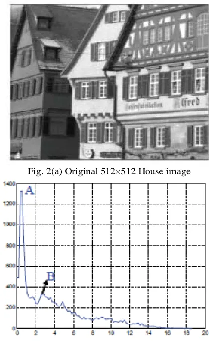
Fig. 2(a) Original 512×512 House image
Fig. 2 (b) Histogram of the gradient magnitude after NMS.
As in [6], it was observed that the largest peak in the gradient magnitude histograms after NMS of the Gaussian smoothed natural.
Fig. 3 Reconstruction values and quantization levels; min and max representation.
549
Copyright © 2011-15. Vandana Publications. All Rights Reserved.
A and B and few quantization levels in other parts. Fig. 3 shows reconstruction levels can be computed.
IV.
PROPOSED DISTRIBUTED CANNY
ALGORITHM IMPLEMENTATION ON
FPGA
In this section, we describe the hardware implementation of our proposed distributed Canny edge detection algorithm on the Xilinx Spartan-3E FPGA.
A. Architecture Overview
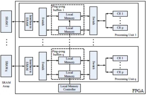
Fig. 4 The architecture of the proposed distributed Canny
Depending on the available FPGA resources, the image needs to be partitioned into q sub-images and each sub-image is further divided into p m x m blocks. The proposed architecture, shown in Fig.4, consists of q processing units in the FPGA and some Static RAMs (SRAM) organized into q memory banks to store the image data.Thus, p × q blocks can be processed at the same time and the processing time for an N×N image is reduced, in the best case, by a factor of p x q.
Fig. 5 compute engine(CE) for the proposed
The specific values of p and q depend on the processing time of each PE, the data loading time from the SRAM to the local memory and the interface between FPGA and SRAM, such as total pins on the FPGA, the data bus width, the address bus width and the maximum system clock of the SRAM.
B. Image Smoothening
The input image is smoothened using a 3×3 Gaussian mask, as shown in Fig. 6(a). The Gaussian filter (Fig. 6a) is separable and, thus, the implementation of the 2-D convolution with the 3×3 Gaussian mask is achieved using row and column 1- D convolutions. The proposed architecture for the smoothening unit is shown in Fig. 6(b).
Fig. 6(a) Mask for the low pass Gaussian filter
Fig. 6 (b) Pipelined Image Smoothening Unit.
The main components of the architecture consists of a 1-D finite impulse filter (FIR) to process the data and the on-chip Block RAM (BRAM) to store the data. In our design, we adopt the Xilinx’s pipelined FIR IP core, which provides a highly parameterizable, area-efficient, high-performance FIR filter utilizing the structure characteristics in the coefficient set, such as symmetry and conjugacy .
C. Gradients and Gradient Magnitude Calculation
550
Copyright © 2011-15. Vandana Publications. All Rights Reserved.
Fig. 7 Gradient and Magnitude Calculation Unit.
D. Directional Non Maximum Suppression
Fig. 8 shows the architecture of the directional NMS unit. In order to access all the pixels’ gradient magnitudes in the 3×3 window at the same time, two FIFO buffers are employed.
Fig. 8.Directional Non Maximum Suppression Unit.
The horizontal gradient Gx and the vertical gradient Gy control the selector which delivers the gradient magnitude (marked as M(x, y) in Fig. 8) of neighbours along the direction of the gradient, into the arithmetic unit. E. Calculation of the hysteresis thresholds:
Since the low and high thresholds are calculated based on the gradient histogram, we need to compute the histogram of the image after it has undergone directional non-maximum suppression .As discussed in Section 3, an 8- step non-uniform quantizer is employed to obtain the discrete histogram for each processed block.
Fig. 9 The architecture of the Threshold Calculation Unit.
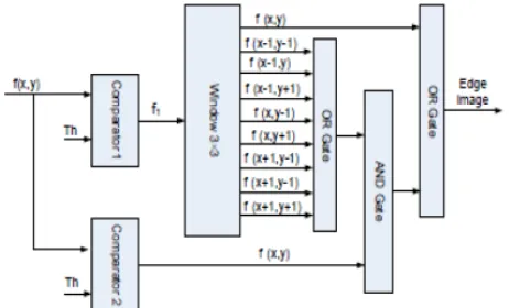
F. Thresholding with hysteresis
Since the output of the non maximum suppression unit contains some spurious edges, the method of thresholding with hysteresis is used. Two thresholds, high threshold ThH and low threshold ThL , which are obtained from the threshold calculation unit, are employed. Let f(x, y) be the image obtained from the non maximum suppression stage, f1(x, y) be the strong edge image and f2(x, y) be the weak edge image.
Fig. 10 Pipelined architecture of the Thresholding unit
V. SIMULATION RESULTS
The algorithm performance was tested using a variety of512×512 natural images.
551
Copyright © 2011-15. Vandana Publications. All Rights Reserved.
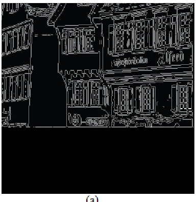
Fig 11. Floating-point Mat lab simulation results for the 512×512 House image(a) Edge map of the original Canny
(b) algorithm of [4] with a 3×3 mask
(c) proposed algorithm with a 3×3 gradient mask and a block-size of 64.
B. Fixed-point Mat lab and FPGA Simulation Results
Fig.12 shows the fixed-point Mat lab implementation software result and the FPGA implementation generated result for the 512×512 House image using the proposed distributed Canny with block size of 64×64 and a 3×3gradient mask. The FPGA result is obtained using Model Sim . Furthermore, for a 100MHz clock rate, the total processing running time using the FPGA implementation is 0.287ms for a 512×512 image.
Fig. 12(a) Edge map of Mat lab implementation;
(b) Edge map of FPGA implementation
VI.
CONCLUSION
552
Copyright © 2011-15. Vandana Publications. All Rights Reserved.
algorithm. The algorithm is mapped to onto a Xilinx Spartan-3E FPGA platform and tested using Model Sim.
REFERENCES
[1] F. M. Alzahrani and T. Chen, “A real-time edge detector algorithm and VLSI architecture,” Real-Time Imaging , vol. 3, no. 5, pp. 363 – 78, 1997.
[2] L. Torres, M. Robert, E. Bourennane, and M. Paindavoine ,“I implementation of a recursive real time edge detector using retiming techniques,”
VLSI, pp. 811 –816,Aug. 1995.
[3] D. V. Rao and M. Venkatesan, “An efficient reconfigurable architecture and implementation of edge detection algorithm using Handle-C,” ITCC,
vol. 2, pp. 843 – 847,Apr. 2004.
[4] S. Varadarajan, C. Chakrabarti, L. J. Karma, and J. M.Bauza , “A distributed psycho-visually motivated Canny edge detector,” IEEE ICASSP, pp.
822 –825, Mar. 2010.
[5] J. Canny, “A computational approach to edge detection,”IEEE Trans. PAMI, vol. 8, no. 6, pp. 679 –698, Nov. 1986.