An Effective Algorithm for Minimizing the Critical
Access Time of a 3D-Chip Data Bus
Chia-Chun Tsai
Dept. of Computer Science and Information Engineering Nanhua University, Chiayi, Taiwan (R.O.C.)
Date of publication (dd/mm/yyyy): 08/07/2018
Abstract – A 3D chip exists a natural 3D data bus that integrates all the local data buses located on different stacked layers by vertically connecting a number of TSVs. The critical access time of running data on the 3D data bus dominants the keyed performance of a 3D chip. This paper conducts to minimize the critical access time on a 3D data bus. Based on the topology of a 3D data bus with a number of timing periods for accessing data, an effective algorithm is proposed to insert signal repeaters into the critical access path of the bus and tune their sizes to minimize the critical access time. This procedure is repeated until no additional improvement. For ten tested 3D data buses with various topologies using 45nm technology, experimentally, our algorithm can effectively reduce the critical access time of a 3D data bus up to 86.14% with inserted repeater sizes of 65 on average.
Keywords – 3D Data Bus, Critical Access Time, Signal
Repeater, TSV.
I.
I
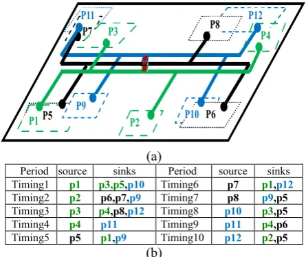
NTRODUCTIONThe design of a SoC (system-on a chip) has been transferred to be a 3D stacked-layer chip [1, 2] with CMOS nanometer technology. A 3D chip has at least two dies and data signals can be accessed between modules on the dies with each other via TSVs (through silicon vias). The chip performance depends on the critical access time of signals propagated on system buses, especially, for the longer data bus. The figure of Fig. 1 illustrates the topology of a 3D data bus that is existed on a 3D stacked-layer chip. The chip contains three dies, Die1, Die2, and Die3. These dies have their respectively four modules and local data bus, and three local data buses are interacted via two TSVs. Data can be transferred from one module to any other modules via local data buses and TSVs in a specific timing period. For example, data can be propagated from the terminal p4 to terminal p11 at a timing period. Also, another data can also be converted from the terminal p11 to terminals p4 and p6 at the other timing period. Notably, terminals p4 and p11 can be viewed as a source or sink in a non-overlapping timing period. Accordingly, the 3D data bus has the characteristics of multiple-source multiple-sink bidirectional transmission.
In a 3D chip, data are frequently running on the 3D data bus at the massive different timing periods. The critical access time among different timing periods dominates the chip performance. Therefore, minimizing the critical access time on a multiple-source and multiple-sink bidirectional 3D data bus is important one of high-performance goals.
P12
P9 P10
P11
P8
P5 P6
P7
P4
P1 P2
P3
TSV1
Die1 TSV2
Die2 Die3
Fig. 1. Typical structure of a 3D data bus in a 3D chip.
Cho et al. [3] presented the analysis of system bus on a multiple-layer SoC considering the interconnection of TSVs. They found the maximum throughput of a 3D system bus depending on the data bandwidth and the number of layers. Tsai et al. [4] first conducted buffer insertion to minimize the maximal propagation delay for a 2D data bus. To evaluate the propagation delay, many approaches [4]-[5] based on Elmore RC delay model [6] have been developed to reduce the interconnect delay. Also, various RLC-based interconnect delay models were proposed to be applied. Ismail et al. [7, 8] was the first to propose empirical formulas for the path delay of a wire and applied it to estimate the delay of on-chip interconnects, as well as considering the inductive effects and inserted repeaters. Chen et al. [9] also introduced complex formulas for the path delay of a transmission line and applied it to a buffer clock tree. Venkatesan et al. [10] utilized the insertion of repeaters in the distributed RLC trees to eliminate crosstalk. Tsai et al. [11] also conducted RLC-based repeater insertion to minimize the maximum delay for a 2D data bus. Ghoneima et al. [12] presented the interleaved repeaters for optimal positioning on bidirectional buses. His solution can reduce the noise interference between 2D data buses.
3D-Copyright © 2018 IJECCE, All right reserved Wiz for reducing the interaction overloading between data
bus of DRAMs. This architecture can reduce the access time to any DRAM. Recently, Tsai [18] proposed alternative approach by inserting bus switches to isolate the unnecessary local buses. This method can reduce the unnecessary capacitive loadings and speed up the data access time.
This work minimizes the critical access time of a 3D data bus existed in a 3D stacked-layer chip. A heuristic algorithm based on repeater insertion and sizing is utilized to repeatedly minimize the critical access time until no any improvement. Experimental results demonstrate that the critical access time of a 3D-chip data bus can be effectively reduced in nanometer technology.
The reminder of this paper is organized as follows. Section II describes the problem formulation. Section III states the evaluation of data access time to the delay model of an equivalent circuit without/with inserted repeaters. Section IV presents the proposed algorithm of critical access time minimization. Section V shows the experimental results of ten tested examples. Finally, Section VI gives summary conclusion for this work.
II.
P
ROBLEMF
ORMULATIONFor a chip, its data bus exhibits the characteristics of data bidirectional access. In general, a repeater that is inserted into a sufficiently long data bus wire can effectively reduce the bus-wire delay. Let tB, rB, and cB be the intrinsic delay,
output driving resistance, and input loading capacitance of a unit-size repeater, respectively. Increasing the repeater size, sB1, will reduce the output resistance of a repeater B1,
rB/sB1, and decrease the driving delay; but, the input
capacitance of a repeater B1, cB*sB1, also increases
simultaneously and potentially, increase the pre-stage driving delay. However, the intrinsic delay tB is independent
of the repeater size [19] and so tB is assumed to be a constant.
The delay reduction of a wire can be easily maximized by carefully sizing the repeater for a one-source one-sink bus wire, even if a bus wiring tree with single-source multiple sinks is applied.
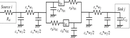
Figure 2 shows a two-source two-sink data bus with a bidirectional repeater inserted into the middle of the bus segment. Fig. 2(b) presents the equivalent circuit of Fig. 2(a), where i and j are the drivers and sinks used in different timing periods. The bidirectional repeater consists of two opposite unidirectional repeaters B1 and B2 in parallel, with
different sizes sB1 and sB2, respectively. The bus segment is
divided two pieces of bus segments, w1, and w2.
Accordingly, one signal is propagated from source i to sink j via the repeater B1 and another is propagated from source
j to sink i via repeater B2. The propagation delay from
source i to sink j, Tij, is the sum of three delays delay tw1
from source i to repeater B1, intrinsic delay tB of repeater B1,
and delay tw2 from repeater B1 to sink j. Therefore, the
propagation delay Tij (or Tji from source j to sink i) based
on the Elmore delay model [6] can be derived as follows.
Tij = tw1+ tB1 + tw2 , (1)
where tw1 Rdi(CLi+Cw1’+cB*sB1)+Rw1(Cw1/2+cB*sB1) and tw2 rB/sB1*(cB*sB2+Cw2+CLj). Rdiis the output resistance of the
source driver i and CLj is the loading capacitance of the sink
j. Rw1 is the resistance of the bus segment w1 and Cw2 is the
capacitance of the bus segment w2.
B1
B2
w2
w1
source/ sink i
source/ sink j
bidirectional repeater B
(a)
CLi Rdj
Rdi
cB*sB1 rB/sB1
tB1
rB/sB2
cB*sB2
tB2
CLj
tw2
tw1
(b)
Fig. 2. (a) A two-source two-sink bus with an inserted bidirectional repeater and (b) its equivalent circuit.
Figure 3 illustrates the problem formulation of a multi-source multi-sink 3D data bus that has twelve terminals, twenty-four bus segments, and ten timing periods. This 3D data bus shown in Fig. 3(a) is compacted from Fig. 1. Each timing period shown in Fig. 3(b) has only one driving source, but at least one loading sinks. For example, the driving source p1 can simultaneously propagate data into three loading sinks p3, p5, and p10 in timing1. Terminal p1 is a driving source in timing1 but is also a loading sink in timing 5. The data bus has twenty-four locations for inserting repeaters to reduce the critical access time as possible.
(a)
Period source sinks Period source sinks Timing1 p1 p3,p5,p10 Timing6 p7 p1,p12
Timing2 p2 p6,p7,p9 Timing7 p8 p9,p5
Timing3 p3 p4,p8,p12 Timing8 p10 p3,p5
Timing4 p4 p11 Timing9 p11 p4,p6
Timing5 p5 p1,p9 Timing10 p12 p2,p5
(b)
Fig. 3. (a) A 3D data bus compacted from Fig. 1 and (b) the bus has 10 timing periods.
In summary, the problem for minimizing the critical access time on the 3D data bus of a 3D stacked-layer chip can be defined as follows.
Given m terminals, n segment locations, and p timing period on a 3D data bus, the objective is to minimize the critical access time Tij,
min(max(Tij)), 1 i, j m. (2)
P12
P8
P6
P7 P4
P2 P3
P5 P1
P9
III. E
VALUATION OFD
ATAA
CCESST
IMETo evaluate the critical access time on the 3D data bus of a 3D stacked-layer chip, the delay model of an interconnect bus-wire and an interconnect bus-wire with inserted repeaters are introduced as follows.
A.
Interconnect Delay
This work estimates the data access time of a 3D data bus based on the signal propagation delay using the Elmore RC delay model. The model considers a bus segment wl that has
a -RC mode with the resistance rw*wl and two half
capacitances of cw*wl/2, where rw and cw represent the
resistance and capacitance of a unit-length segment, respectively. We suppose that a TSV has the equivalent -RC mode with the resistance rTSV and two half capacitances of cTSV/2. When the effect of on a 3D data bus is determined, the RC equivalent model is the scaled 50%-scaled propagation delay. Propagation delay Tij from source
i to sink j can be expressed as follows.
Tij = Rik Ck , (3)
where k is a node on the path from source i to sink j. Rik is
the common resistance along the path from node i to k in the RC tree and Ck is the lumped capacitance at node k of
the RC tree.
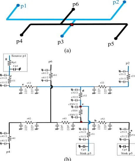
Figure 4 shows a 3D data bus topology that has a TSV to vertically connect two different local buses. Data are delivering from source p1 to two sinks p3 and p5 at a time period and terminals p2, p4, and p6 are isolated from the data bus at the same timing period. Fig. 4(b) presents the equivalent structure of RC-based delay model of Fig. 4(a) for evaluating their access times.
Depending on Eq. (3), the step by step for calculating the delay Tp1-p5 from sink p5 back to source p1 in Fig. 4(b) is
presented as below.
At node a, the lumped capacitance Ca = Cp5+c51/2 and the present delay Ta = r51(Ca).
At node b, Cb = Ca + c51/2 + c52/2 and Tb = Ta + r52(Cb).
At node c, Cc = Cb + c52/2 + c43 + c42 + c41 + c61 + cTSV/2 and Tc = Tb + rTSV (Cc).
At node d, Cd = Cc + cTSV/2 + Cp3 + c31 + c32/2 and Td = Tc + r32 (Cd).
At node e, Ce = Cd + c32/2 + c22 + c21 + c12/2 and Te = Td + r12 (Ce).
At node f, Cf = Ce+c12/2+c11/2 and Tf = Te +r11(Cf). At node g, Cg = Cf+c11/2+Cp1 and Tg = Tf +Rp1(Cg). Therefore,
Tp1-p5 = Tg = Rp1 (Cp5 + c51 + c52 + c43 + c42 + c41 +
c61 + cTSV + Cp3 + c31 + c32 + c22 + c21 + c12 + c11 + Cp1) + r11(Cp5 + c51 + c52 + c43 + c42 + c41 + c61 + cTSV + Cp3 + c31 + c32 + c22 + c21 + c12 + c11/2) + r12(Cp5 + c51 + c52 + c43 + c42 + c41 + c61 + cTSV + Cp3 + c31 + c32 + c22 + c21 + c12/2) + r32(Cp5 + c51 + c52 + c43 + c42 + c41 + c61 + cTSV + Cp3 + c31 + c32/2) + rTSV(Cp5 + c51 + c52 + c43 + c42 + c41 + c61 + cTSV/2) + r52(Cp5 + c51 + c52/2) +
r51(Cp5+c51/2) (4)
p4
p6 p2
p1 p3 p5 (a) cTSV/2 cTSV/2 p4 Source p1
p6 p2
Sink p3 c61/2 c61/2 Cp1 r11 c11/2 c11/2 r21 c21/2 c21/2 r12 c31/2
c31/2 r31
c41/2
c41/2 r41
r32
c51/2
c51/2 r51
rTSV c32/2 c32/2 r22 c1 2/2 c1
2/2 c22/2 c22/2
c2 2/2 c2 2/2 r42 c4 3/2 c4 3/2 r43 c5 2/2 c5 2/2 r52 r61
Cp3 Cp5
Rp1 Sink p5 b g f e d c a (b)
Fig. 4. (a) Data are delivered from source p1 to sinks p3 and p5 in a timing period, but other sinks are isolated from
the bus, and (b) its equivalent RC model.
It is noted that the delay is accounted for the cases of from sink j back to source i at the intersection of a TSV. Figure 5 shows their two cases of Fig. 4(b).
r2 rTSV cTSV/2 cTSV/2 c2 /2 c2 /2 c1/2 x V2
Cx and Tx at node x from sink j
Lumped capacitance CV1 at node V1 of
the subtree
y
V1
Cy and Ty at node y from sink j toward source i
(a) r2 rTSV cTSV/2 cTSV/2 c2 /2 c2 /2 c1/2 x V2
Cx and Tx at node x from sink j
Lumped capacitance Ck at node k of the subtree
y
V1
Cy and Ty at node y from sink j
toward source i
k
(b)
Fig. 5. (a) Case1: the resistance rTSV of a TSV is not located on the delay path from x to y and (b) case2: the
Copyright © 2018 IJECCE, All right reserved For case1 in Fig. 5(a), the delay path is from node x to
node y and toward the source i, but the resistance of rTSV is not located on the path and cannot be accounted in the delay, that is, the lumped capacitance Cy = Cx + c1/2 + cTSV/2 + CV1 + cTSV/2 + c2/2 and the delay Ty = Tx + r2(Cy) at node
y. For case2 in Fig. 5(b), the delay path from node x toward node y and the resistance of rTSV is along the path and should be accounted into the delay, that is, the lumped capacitance CV2 = Cx + c1/2 + cTSV/2 and the delay TV2 =
rTSV (CV2) at node V2 and then, the lumped capacitance Cy
= CV2 + cTSV/2 + Ck + c2/2 and the delay Ty = Tx + r2(Cy)
at node y.
B.
Delay with Inserted Repeaters
Generally, a buffer can be replaced by a unidirectional repeater. A bidirectional repeater [19] has two unidirectional repeaters that are connected opposite with each other in parallel, provides the advantage of directing signal transition. We employ a bidirectional repeater as our signal repeater model. An extra signal of this repeater is not required to control the direction of signal propagation. The repeater can detect the transmission direction change automatically and reconfigure itself.
Figure 6 shows the equivalent delay model for the bus segment w with a bidirectional repeater inserted into the middle of the segment, where Rdi is the resistance of the
driver source i; CLj is the load capacitance of sink j. The
wire segment w is divided into two sub-segments, w1 and
w2, where rw*w1 and cw*w1 are the respectively resistance
and capacitance of w1, and rw*w2 and cw*w2 are the
respectively resistance and capacitance of w2. The
bidirectional repeater consists of two opposite unidirectional repeaters in parallel, B1 and B2, where tB1,
rB/sB1, and cB*sB1 are the intrinsic delay, output resistance,
and input capacitance of the unidirectional repeater B1 with
the size of sB1, respectively, and tB2, rB/sB2, and cB*sB2 are
the intrinsic delay, output resistance, and input capacitance of the unidirectional repeater B2 with the size of sB2,
respectively.
Rdi
cw*w1/2
tB1
rB/sB2
cB*sB1
tB2
Sink j rw*w1
CLj
Source i
cw*w1/2
rB/sB1
cB*sB2 c w*w2/2
rw*w2
cw*w2/2
Fig. 6. Equivalent delay model with a bidirectional repeater inserted into the middle of a wire w.
The propagation delay Tij from source i to sink j based on
Eqs. (1), (3), and (4) is derived as
Tij = rw*w2 (CLj+cw*w2/2) + rB/sB1(CLj+cw*w2+cB*sB2) +
tB1+ rw*w1 (cB*sB1+cw*w1/2) + Rdi(cB*sB1+cw*w1).
(5)
From Eq. (5), the propagation delay Tij can be reduced
significantly by the unidirectional repeater B1, as the output
resistance of the repeateris reduced by the size of sB1, rB/sB1.
However, delay Tij is also increased slightly due to the
effects of their two input capacitors. One capacitor is the input capacitance of the repeater B1, which is increased by
the size of sB1, cB/sB1, and another is the input capacitance
of the other unidirectional repeaterB2, which is increased
by the size of sB2, cB/sB2. Hence, the sufficient and necessary
condition for reducing the propagation delay Tij is that the
effect of the reduced output resistance rB/sB1 must overcome
the effect of two increased capacitances cB/sB1 and cB/sB2.
Therefore, the repeater B1 must be sized carefully to
maximally reduce the delay of Tij.
Similarly, if the propagation direction of a signal is from source j to sink i, then the equivalent delay model is analogous to that in Fig. 6. That is, Rdj is located on the right
side of the figure as the output resistance of source j, and CLi is located on the left side of the figure as the load
capacitance of sink i. Then, the resistances and capacitances of two sub-wire segments are placed in order from right to left. Accordingly, propagation delay Tji from source j to sink
i is calculated as
Tij = rw*w1 (CLi+cw*w1/2) + rB/sB2(CLi+cw*w1+cB*sB1) +
tB2+ rw*w2 (cB*sB2+cw*w2/2) +Rdj(cB*sB2+cw*w2).
(6)
Thus, appropriately sizing the unidirectional repeater B2
can also reduce the propagation delay of Tji.
The propagation delays given by Eqs. (5) and (6) for a bus segment with an inserted bidirectional repeater can be extended to an entire multi-source multi-sink RC-based 3D data bus with inserted repeaters. For a 3D data bus with a number of timing periods, there are many Eqs. (5) and (6) Tij-like equations to be derived. These equations have the
potential numerical problems, such as determining the best location order along the critical path for inserting repeaters and their sizing order for sizing all the inserted repeaters, to be solved for minimizing the maximal access time, i.e., min (max (Tij)). Solving this problem by numerical methods is
very difficult and it was proved to be intractable [4].
IV.
A
LGORITHM FORM
INIMIZINGC
RITICALA
CCESST
IMEThe algorithm of 3D_DataBus_AccessTime_Min() is proposed in Fig. 7 for solving the above problem min(max(Tij)) of a 3D data bus topology with n
bus-segments (i.e., locations for inserting repeaters) and p timing periods. The algorithm is consisted of two major functions. One is Find_Critical_AccessPath() and the function always finds the current critical access path with the maximum access time from all the timing periods and gets a number of k bus-segments along the critical path for preparing repeater insertion. The other is Tune_Repeater() and the function tries to insert repeaters into the number of k bus-segments along the current critical access path and then size the repeaters for reducing the critical access time as possible. The above process is repeated by the repeat loop until no additional improvement. Finally, minimizing the critical access time can be achieved.
3D_DataBus_AccessTime_Min (n,p)
{ repeat
Critical_AccessTime = Find_Critical_AccessPath (n,p,k); /* k is a return value which is #segments along critical path.*/ pre_Critical_AcessTime = Critical_AccessTime;
pre_max_AccessTime = MAX;
for (y = 1 to k)
{ Let rnbe repeaters inserted into current critical access path;
if (segment y has not inserted any repeaters yet)
rn = rn+1; /* insert new repeater into the middle of y */
max_ AccessTime = Tune_Repeater (rn);
if (max_AccessTime < pre_max_AccessTime)
pre_max_ AccessTime = max_AccessTime;
}
Critical_AccessTime = pre_max_AccessTime;
if (Critical_AccessTime < pre_Critical_AccessTime)
Store inserted repeater data including locations and sizes.
until Critical_AccessTime pre_Critical_AccessTime
}
Fig. 7. Algorithm for minimizing critical access time on a 3D data bus.
The function Find_Critical_Delay() is presented in Fig. 8 that purpose is to determine a new critical path with maximum propagation delay and the total number of k bus-segments along the current critical path for timing periods. Then, return k locations for inserting repeaters and critical delay to the above algorithm.
Find_Critical_AccessPath (n,p,k)
{ critical_delay = MIN;
for m = 1 to p
{ Let i be source and j be sink for current timing period; Construct the RC-based equivalent delay model for n segments like And calculate the current delay Tij from sink j back to source i;
If (current_delay > critical_delay) { critical_delay = current_delay;
Store critical_delay and number of k (kn) segments along the current critical path;
}
}
Return critical_delay & k segments;
}
Fig. 8. The function of Find_Critical_AccessPath.
The function Tune_Repeater() is shown in Fig. 9 that purpose is utilized to size rn repeaters until the current
critical delay cannot be improved further. A unit-size repeater is first inserted into the middle of segment y, and then the repeater is sized until the delay of adjust_critical_delay cannot be reduced. Sub-function Repeater_Sizing() sizes a repeater that has been inserted into one possible segment y along the critical path to minimize the critical delay. The repeater is sized from x1 to x16 to maximize the reduction in the delay each time. Consequently, Repeater_Sizing() can minimize the critical delay using the sized repeater. The purpose of each repeat loop in Tune_Repeater() is to repeatedly minimize the critical delay and to converge when adjust_critical_delay cannot be reduced.
The time complexity of the proposed algorithm is
analyzed as follows. The function of
Find_Critical_AccessPath() determines the current critical access time from all sources to all sinks and no more than n2 segments are visited from the sources to the sinks at each
timing period. Thus, the execution time is O(p*n2), where p
is the number of periods and n is the number of segments. The other function Tune_Repeater() iterates rn times to size
a repeater that is inserted into each possible segment y to reduce the critical access time and its time complexity is O(M*p*n4) [4], where M is the maximum repeater size.
The primary procedure has a for-loop that runs at most k times. Given k = O(n), therefore, the time complexity of the proposed algorithm is O(M*p*n5).
Tune_Repeater (rn)
{repeat
fory = 1 to rn
{ repeat
if (segment y has the direction toward left/down (or right/up)) { y.size = y. sB1 (or y. sB2) = 1;
repeat // sizing one unidirectional repeater adjust_critical_delay = Repeater_Sizing(y.size); until adjust_critical_delay cannot be reduced }
until adjust_critical_delay cannot be reduced
}
until adjust_ctitical_delay cannot be reduced return (adjust_critical_delay);
}
Fig. 9. The function of Tune_Repeater.
V.
E
XPERIMENTALR
ESULTSThe algorithm was implemented in C language on an i7 CPU@2GHz, dual cores with 8GB RAM, running MS-Windows 10. Table 1 shows the parameters of 45 nm technology [20] based on Elmore RC delay model [6]. The terms rw and cw represent the resistance and capacitance of
a unit-length wire, respectively; rTSV and cTSV state the resistance and capacitance of a TSV, respectively; rB, cB,
and tB denote the output resistance, input capacitance, and
intrinsic delay of a unit-size unidirectional repeater, respectively.
Table 1. The parameters based on 45nm technology [20].
rw(Ω/) cw(fF/μm2) rTSV(Ω) cTSV(fF) rB(Ω) cB(fF) tB(ps)
0.1 0.2 0.035 15.48 122 24 17
Currently, we have not find any standard benchmarks of 3D data bus, ten 3D data bus topologies are created for testing our proposed algorithm. For simplicity, the driving resistance Rd of all sources and the loading capacitance CL
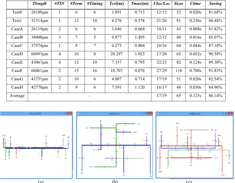
of all sinks are assumed to their parameters of a unit-sized repeater. An inserted repeater size can be adjusted by binary search from x1 to x16. Table 2 shows their experimental results. Tlength is the total length of a 3D data bus, and #TSV, #Term and #Timing are the number of TSVs, terminals and timing periods, respectively. Tcri and Tmax are the critical access times without and with inserted repeaters, respectively, and Uloc and Loc are the number locations of inserted repeater and the number of available locations, respectively. The ratio of Uloc/Loc is called the inserted repeater ratio. Sizes is the sum of all inserted repeater sizes; Ctime is the running time, and Saving is given as the percentage of (Tcir-Tmax)/Tcri.
Copyright © 2018 IJECCE, All right reserved although all the inserted repeaters may increase power
consumption. The tradeoff between critical access time minimization and inserted repeater sizes still depends on a 3D data bus topology.
The first test case in Table 2, Test 0, is shown in Fig. 4 as for estimating the access time of an equivalent circuit delay model in Section II.A. The second test case, Test1, is the right figure of Fig. 3 as for the analysis of our problem formulation in Section II.
Figures 10(a), 10(b), and 10(c) show their results of Test1, CaseE and CaseF, respectively. For Test1, the 3D data bus has one TSV, twelve terminals, and twenty-six segments. The inserted repeater ratio is 21/26 including 19 bidirectional repeaters and 2 unidirectional repeaters. Two numbers in the figure closed to the middle of a segment are the sizes of an inserted bidirectional repeater. Only one number represents the size of an inserted unidirectional repeater. Critical access times without and with inserted repeaters are 4.276 ns from source p4 to sink p11 and 0.578 ns from source p11 to sink p4, respectively. The saving in the critical access time is up to 86.48% ((4.276-0.578)/4.276) with the number of inserted repeater sizes, 81. For CaseE, the 3D bus topology has four TSVs, twelve terminals, and twenty-three segments. Nineteen bidirectional repeaters and three unidirectional repeaters are inserted in twenty-three locations. Critical delays without and with inserted repeaters are 7.337ns from source p7 to sink p2 and 0.795ns from source 1 to sink 9, respectively. The reduction in the critical delay with inserted repeaters is 89.3% when the repeater sizes of 82 are used. For CaseF, the 3D data bus has two TSVs, fifteen terminals, and twenty-nine segments. Critical delays without and with inserted repeaters are 10.707ns and 0.876ns from source p13 to sink p1, respectively. The reduction in the critical delay with inserted repeater sizes of 110 is up to 91.83%.
VI.
C
ONCLUSIONThe proposed algorithm has successful to apply the 3D data bus of a stacked-layer chip and it can significantly reduce the critical access time of the bus. The algorithm is simple and very effective and it can be used to make post-layout refinement to promote a 3D chip performance. Inserting repeaters into a 3D-chip data bus in post step may be a little difficult in practical because the chip space is limited and the netlist must be changed. Alternatively, the algorithm can be employed for estimating the chip performance followed the minimization of critical access time during the floorplanning or placement step in the physical design.
A
CKNOWLEDGMENTThis work was supported by MOST 105-2221-E-343-004 and NHU-106 research project. The author would like to thanks for their financial supports.
R
EFERENCES[1] Charles Chiang and Subarna Sinha, “The road to 3D EDA tool readiness,” IEEE/ACM ASP-DAC, 2009, pp. 429-436. [2] EE Times, “The state of the art in 3D IC technologies,” Nov. 27,
2013.
[3] Kyoungrok Cho, Hyeon-Seok Na, Tae Won Cho, and Younggap You, “Analysis of system bus on SoC platform using TSV interconnection,” The 4th Asia Symposium on Quality Electronic Design, 2012, pp. 255-259.
[4] Chia-Chun Tsai, De-Yu Kao, and Chung-Kuan Cheng, “Performance driven bus buffer insertion,” IEEE Trans. on CAD of Integrated Circuits and Systems, Vol. 15, No. 4, 1996, pp. 429-437.
[5] Jason Cong, and D. Z. Pan, “Interconnect delay estimation models for synthesis and design planning,” IEEE/ACM ASP-DAC, 1999, pp. 97-100.
[6] W. C. Elmore, “The transient response of damped linear networks,” Journal of Applied Physics, Vol. 19, 1948, pp. 55-63.
[7] Y. I. Ismail, E. G. Friedman, and J. L. Neves, Equivalent Elmore delay for RLC trees, IEEE Trans. on CAD of Integrated Circuits and Systems, 2000, pp. 83-97.
[8] Y. I. Ismail and E. G. Friedman, “Effects of inductance on the propagation delay and repeater insertion in VLSI circuits,” IEEE Transactions on Very Large Scale Integration Systems, Vol. 8, 2000, pp. 195-206.
[9] Tai-Chen Chen, Song-Ra Pan, and Yao-Wen Chang, “Performance optimization by wire and sizing under the transmission line model,” International Conference on Computer Design, 2001, pp. 23-26.
[10] R. Venkatesan, J. A. Davis, and J. D. Meindl, “Compact distributed RLC interconnect models - part IV: unified models for time delay, crosstalk, and repeater insertion,” IEEE Transactions on Electron Devices, Vol. 50, 2003, pp. 1094-1102.
[11] Chia-Chun Tsai, Jan-Ou Wu, and Trong-Yen Lee, “Maximal delay reduction for RLC-Based multi-source multi-sink bus with repeater insertion,” Circuits, Systems & Signal Processing, Vol. 28, 2009, pp. 805-817.
[12] Maged Ghoneima and Yehea Ismail, “Optimum positioning of interleaved repeaters in bidirectional buses,” IEEE Trans. on CAD of Integrated Circuits and Systems, Vol. 24, 2005, pp. 461-669. [13] Chia-Chun Tsai, “Repeater insertion for 3D data bus with TSVs
for reducing critical propagation delay,” International Conference on Computer Science and Information Engineering, June 28-29, 2015, pp. 203-208.
[14] Chia-Chun Tsai, “A heuristic algorithm for critical access time minimization on 3D data bus,” The 27th VLSI Design/CAD Symposium, Aug. 2-5, 2016, Paper ID:182.
[15] M. Daneshtalab, M. Ebrahimi, and J. Plosila, “HIBS- Novel Inter-layer Bus Structure for Stacked Architectures,” IEEE International Conf. on 3D System Integration, 2012, pp. 1-7. [16] Y. Shiraishi, M. Hashiume, and H. Yotsuyanagi, “Electrical test
method of open defects at data buses in 3D SRAM IC,” IEEE international Conf. on Electrics Packaging, 2014, pp. 235-238. [17] Ishan G Thakkar and Sudeep Pasricha, “3D-Wiz: A novel high
bandwidth, optically interfaced 3D DRAM architecture with reduced random access time,” IEEE International Conf. on Computer Design, 2014, pp. 1-7.
[18] Chia-Chun Tsai, “Minimizing critical access time for 3D data bus based on inserted bus switches and repeaters,” IEEE Computer Society Annual Symposium on VLSI (ISVLSI), July 3-5, 2017, pp. 140-145.
[19] De-Yu Kao, Chia-Chun Tsai, Chung-Kuan Cheng, and Ting-Ting Lin, “New design and implementation for signal repeaters,” The Sixth VLSI Design/CAD Workshop, 1995, pp. 173-176. [20] Tak-Yung Kim and Taewhan Kim, “Clock tree synthesis with
A
UTHOR’
SP
ROFILEChia-Chun Tsai received his B.S. degree in Industrial Education from National Taiwan Normal University, Taipei, Taiwan, ROC, in 1978, and both M.S. and Ph.D. degrees in Electrical Engineering from National Taiwan University, Taipei, Taiwan, ROC, in 1987 and 1991, respectively. From 1978 to 1989, he was a specialist teacher of electronic maintenance at Taiwan Provincial Hsin-Hua and Taipei Municipal Nan-Kang
Technology High Schools, respectively. From 1989 to 2005, he served at the Department of Electronic Engineering, National Taipei University of Technology, Taipei, Taiwan, ROC. From 1994 to 1995 and 2000 to 2001, he was on leave from National Taipei University of Technology and worked on postdoctoral research at University of California, San Diego, and North Carolina State University, respectively. Since 2005 he has been with the Department of Computer Science and Information Engineering, Nanhua University, Chiayi, Taiwan, ROC, where he is a Full Professor. His current research interests include VLSI design automation and mixed-signal IC designs.
Table 2. Results of 3D data bus for ten test cases.
Tlength #TSV #Term #Timing Tcri(ns) Tmax(ns) Uloc/Loc Sizes Ctime Saving
Test0 26188μm 1 6 6 3.891 0.713 12/12 52 0.020s 81.68%
Test1 32314μm 1 12 10 4.276 0.578 21/26 81 0.236s 86.48%
CaseA 26119μm 2 6 6 3.646 0.664 10/11 43 0.008s 81.82%
CaseB 38000μm 3 7 5 9.977 1.495 12/12 48 0.016s 85.07%
CaseC 37574μm 1 9 7 6.273 0.804 16/16 64 0.044s 87.18%
CaseD 60493μm 4 10 8 20.297 1.923 17/20 65 0.052s 90.58%
CaseE 43067μm 4 12 10 7.337 0.795 22/23 82 0.124s 89.30%
CaseF 60461μm 2 15 16 10.707 0.876 27/29 110 0.700s 91.83%
CaseG 43751μm 2 10 6 4.087 0.714 17/19 51 0.020s 82.54%
CaseH 42770μm 2 9 6 7.391 1.120 16/17 48 0.030s 84.96%
Average - 17/19 65 0.125s 86.14%
(a) (b) (c)