Design of Low Power Flip-Flop Using
Topological Compression Technique
Sudha.H1, Sahana Uppin2
Associate Professor, Dept. of ECE, BIT College, Bangalore, Karnataka, India1
PG Student [VLSI and Embedded System], Dept. of ECE, BIT College, Bangalore, Karnataka, India2
ABSTRACT:As transistor dimensions continues to shrink and increase market trends, extremely required minimized power consumption in modern circuits. In integrated circuit, generally more than half of power is dissipated in random logic, of which half of the power is dissipated by flip-flop. In proposed system mainly focused on power saving and design with less transistor count. The topological compression technique is applied to achieve power reduction such that merging of logically equivalent transistor to an unconventional latches structure. The transistor count is reduced because only three, connected to clock signal which reduce the power consumption and smaller sum of transistor count assures less chip area as compare conventional flip-flop. The sleep transistor with TCFF helps to reduce power further. The proposed system is designed and implementation had been carried out with 32nm CMOS technology shows almost all conventional flip-flop are replaced with proposed flip-flop.
KEYWORDS: low power, TCFF, sleep transistor.
I.INTRODUCTION
The market trend keeps on expanding day by day which has demanded for reduction power in portable device. For example mobile phone, digitals camera, tablet PC, development with various advance features and technology. For such battery-working equipment require small amount of power. In all type of portable electronic design requirement is reduction in weight and size of device which is concentrated by the number of power source used and their lifetime. In addition to fulfil the requirement with advance technology goes for tumbling the transistor size, reducing supply voltage, more complexity chip design which give rise to larger amount of power dissipation. Therefore due to this all reason there has been increased demand for need of CMOS low-power design. The memory device application has been widespread in a market which needs low consuming power.
I
nternational
J
ournal of
A
dvanced
R
esearch in
E
lectrical,
E
lectronics and
I
nstrumentation
E
ngineering
(An ISO 3297: 2007 Certified Organization)
Vol. 5, Issue 5, May 2016
II.LITERATURE SURVEY
.
Fig 1 Conventional transmission-gate flip-flop
Literature survey gives brief idea of on analyse of typical low-power flip-flop and limitation as compare to conventional flip-flop shown in fig 1
Fig 2:Differential sense-amplifier flip-flop (DiffFF).
Fig 2 shows differential sense-amplifier, it is used to amplify a small voltage difference between signals. It is widely used in semiconductor memory device, in order to read the data stored in memory cell, decode the read out data and amplify the data which is being read out. This type of flip-flop as pre-charge operation in every clock-low state hence the condition of lower data activity goes down with reduction power. A extra bias circuit and customized clock generator is required if use reduced clock swing which result in more power dissipation.
Fig 3: Conditional-clocking flip-flop
Fig 4 cross-charge flip-flop
Fig 4 shows cross-charge control flip-flop, it has two dynamic nodes, where first node is connected to the gate of output transistor through an inverter circuit and second node is directly connected to the output transistor. It is used drive output transistor separately in order to charging and discharging of gate capacitance. During actual operation, when data is high, some of internal nodes are pre-set with clock signal which result in extra power dissipation to charge and discharge internal nodes. The problem associate with circuit is pre-set operation.
.
Fig 5 Adaptive-coupling type flip-flop
Fig 5 shows adaptive-coupling type flip-flop, it consist six transistor memory cells and single-channel transmission gate with additional dynamic circuit is used for a data line in order to reduce clock related transistor count. The single channel transmission gate and dynamic circuit are affect by process variation thus, their optimization is difficult and performance degradation
III.PROPOSED SYSTEM
In proposed system, in order to reduce power dissipation of the flip-flop and keeping competitive performance and same cell area, we tried to reduce transistor count those operating with clock signals.
Fig 6 Schematic of proposed flip-flop
I
nternational
J
ournal of
A
dvanced
R
esearch in
E
lectrical,
E
lectronics and
I
nstrumentation
E
ngineering
(An ISO 3297: 2007 Certified Organization)
Vol. 5, Issue 5, May 2016
Fig 7 Transistor level of proposed flip-flop
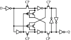
The proposed system transistor level flip-flop is shown in fig 7,to reduce transistor count based on logical equivalence, we consider a method that consists of two step, first step, the circuit with two or more logically equivalent And or OR logic parts which have the same input signal combinational , including especially input signal as clock signal. Second step, merge those parts in transistor level. The merging process to original circuit result as shown in fig 8, which consist of less seven transistor as compare to original circuit and three clock-related transistor. There is no additional power dissipation because no dynamic circuit and pre-charge circuit.
Fig 8 Topologically compressed flip-flop
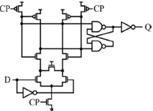
This circuit consists of two different type latches in the master and salve. The main feature of this circuit is that it operates in single phase and it has two set of logically equivalent input. The master-latch is asymmetrical single data input and salve-latch is known as rest-set type. When CP is low, the PMOS connected to transistor CP turn ON and NMOS is turn OFF, mater latch is input mode. Both voltage supply (VD1 and VD2) are pulled up to power supply level and input data stored in master-latch. When CP is high, the PMOS transistor connected to CP turn OFF and NMOS turn ON and slave latch becomes data output mode. In this condition, data stored in master latch is transferred to slave latch and then to output Q.
between pull down network and ground for high switching speed, when it is low transistor are used in circuit. Efficient power management is done by sleep control mechanism.
IV.EXPERIMENTAL RESULT
The schematic and simulation result of proposed system
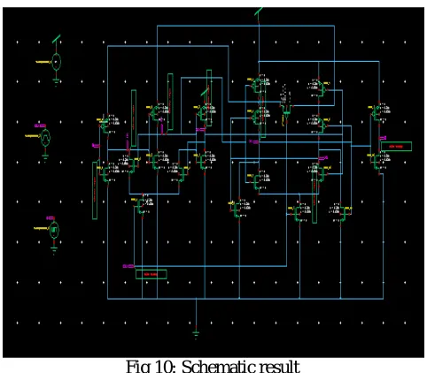
1. Topologically compressed flip-flop
Fig 10: Schematic result
The fig 10 show schematic design of Topologically compressed flip-flop using tanner tool.
Fig 11: Simulation result
I
nternational
J
ournal of
A
dvanced
R
esearch in
E
lectrical,
E
lectronics and
I
nstrumentation
E
ngineering
(An ISO 3297: 2007 Certified Organization)
Vol. 5, Issue 5, May 2016
Fig 12: Power analysis
The fig 12 show power analysis, which consist of power consume of proposed system
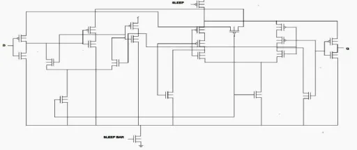
2. Topologically compressed flip-flop with sleep transistor
Fig 13: Schematic result
The fig 13 show schematic design of topologically compressed flip using sleep transistor. The design contains less power consumption than TCFF.
Fig 14 : Simulation result
Fig 15: power analysis
The fig 15 show power analysis, which consist of power consume of proposed system
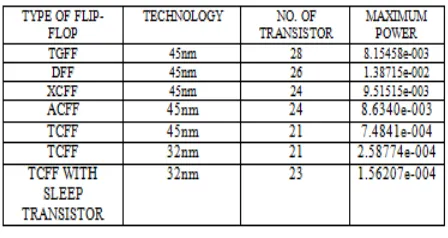
Table 1: Power comparison between flip-flops
This table show power consumption of different flip-flops. By this table it show that power dissipated by proposed system is less as compare to pervious system
V. CONCULSION
An extremely low-power flip-flop, TCFF is proposed with topological compression design methodology. TCFF has the lowest power dissipation in almost all range of the data activity as compared with other low-power flip-flop.the power dissipation through TCFF is less than compare with pervious technique used. TCFF with sleep transistor, power dissipation is lesser than that of TCFF. Hence by proposed system we achieved low power
REFERENCES
[1] H. Kawaguchi and T. Sakurai, “A reduced clock-swing flip-flop (RCSFF) for 63% power reduction,” IEEE J. Solid-State Circuits, vol.33, no. 5, pp. 807–811, May 1998.
[2] J.-C. Kim, S.-H. Lee, and H.-J. Park, “A low-power half-swingclocking scheme for flip-flop with complementary gate and source drive,” IEICE Trans. Electronics, vol. E82-C, no. 9, pp. 1777–1779,Sep. 1999.
[3] M. Matsui, H. Hara, Y. Uetani, L. Kim, T. Nagamatsu, Y. Watanabe, A. Chiba, K.Matsuda, and T. Sakurai, “A 200 MHz 13 mm 2-D DCT macrocell using sense-amplifying pipeline flip-flop scheme,” IEEE J.Solid-State Circuits, vol. 29, no. 12, pp. 1482–1490, Dec. 1994.
[4] M. Hamada, H. Hara, T. Fujita, C.-K. Teh, T. Shimazawa, N. Kawabe, T. Kitahara, Y. Kikuchi, T. Nishikawa, M. Takahashi, and Y. Oowaki,“A conditional clocking flip-flop for low power H.264/MPEG-4 audio/visual codec LSI,” in Proc. IEEE CICC, 2005, pp. 527–530.
[5] Y. Ueda, H. Yamauchi,M.Mukuno, S. Furuichi,M. Fujisawa, F. Qiao,and H. Yang, “6.33 mW MPEG audio decoding on a multimedia processor,”in IEEE ISSCC Dig. Tech. Papers, 2006, pp. 1636–1637.